EP1339009A2 - Fingerprint sensor apparatus and manufacturing method thereof - Google Patents
Fingerprint sensor apparatus and manufacturing method thereof Download PDFInfo
- Publication number
- EP1339009A2 EP1339009A2 EP02257538A EP02257538A EP1339009A2 EP 1339009 A2 EP1339009 A2 EP 1339009A2 EP 02257538 A EP02257538 A EP 02257538A EP 02257538 A EP02257538 A EP 02257538A EP 1339009 A2 EP1339009 A2 EP 1339009A2
- Authority
- EP
- European Patent Office
- Prior art keywords
- semiconductor chip
- sensor part
- fingerprint
- sensor
- resin
- Prior art date
- Legal status (The legal status is an assumption and is not a legal conclusion. Google has not performed a legal analysis and makes no representation as to the accuracy of the status listed.)
- Granted
Links
Images







Classifications
-
- G—PHYSICS
- G06—COMPUTING OR CALCULATING; COUNTING
- G06V—IMAGE OR VIDEO RECOGNITION OR UNDERSTANDING
- G06V40/00—Recognition of biometric, human-related or animal-related patterns in image or video data
- G06V40/10—Human or animal bodies, e.g. vehicle occupants or pedestrians; Body parts, e.g. hands
- G06V40/12—Fingerprints or palmprints
- G06V40/13—Sensors therefor
- G06V40/1306—Sensors therefor non-optical, e.g. ultrasonic or capacitive sensing
-
- H—ELECTRICITY
- H10—SEMICONDUCTOR DEVICES; ELECTRIC SOLID-STATE DEVICES NOT OTHERWISE PROVIDED FOR
- H10W—GENERIC PACKAGES, INTERCONNECTIONS, CONNECTORS OR OTHER CONSTRUCTIONAL DETAILS OF DEVICES COVERED BY CLASS H10
- H10W74/00—Encapsulations, e.g. protective coatings
- H10W74/01—Manufacture or treatment
-
- H—ELECTRICITY
- H10—SEMICONDUCTOR DEVICES; ELECTRIC SOLID-STATE DEVICES NOT OTHERWISE PROVIDED FOR
- H10W—GENERIC PACKAGES, INTERCONNECTIONS, CONNECTORS OR OTHER CONSTRUCTIONAL DETAILS OF DEVICES COVERED BY CLASS H10
- H10W72/00—Interconnections or connectors in packages
- H10W72/50—Bond wires
- H10W72/551—Materials of bond wires
- H10W72/552—Materials of bond wires comprising metals or metalloids, e.g. silver
- H10W72/5522—Materials of bond wires comprising metals or metalloids, e.g. silver comprising gold [Au]
-
- H—ELECTRICITY
- H10—SEMICONDUCTOR DEVICES; ELECTRIC SOLID-STATE DEVICES NOT OTHERWISE PROVIDED FOR
- H10W—GENERIC PACKAGES, INTERCONNECTIONS, CONNECTORS OR OTHER CONSTRUCTIONAL DETAILS OF DEVICES COVERED BY CLASS H10
- H10W72/00—Interconnections or connectors in packages
- H10W72/851—Dispositions of multiple connectors or interconnections
- H10W72/874—On different surfaces
- H10W72/884—Die-attach connectors and bond wires
-
- H—ELECTRICITY
- H10—SEMICONDUCTOR DEVICES; ELECTRIC SOLID-STATE DEVICES NOT OTHERWISE PROVIDED FOR
- H10W—GENERIC PACKAGES, INTERCONNECTIONS, CONNECTORS OR OTHER CONSTRUCTIONAL DETAILS OF DEVICES COVERED BY CLASS H10
- H10W74/00—Encapsulations, e.g. protective coatings
- H10W74/10—Encapsulations, e.g. protective coatings characterised by their shape or disposition
-
- H—ELECTRICITY
- H10—SEMICONDUCTOR DEVICES; ELECTRIC SOLID-STATE DEVICES NOT OTHERWISE PROVIDED FOR
- H10W—GENERIC PACKAGES, INTERCONNECTIONS, CONNECTORS OR OTHER CONSTRUCTIONAL DETAILS OF DEVICES COVERED BY CLASS H10
- H10W90/00—Package configurations
- H10W90/701—Package configurations characterised by the relative positions of pads or connectors relative to package parts
- H10W90/731—Package configurations characterised by the relative positions of pads or connectors relative to package parts of die-attach connectors
- H10W90/734—Package configurations characterised by the relative positions of pads or connectors relative to package parts of die-attach connectors between a chip and a stacked insulating package substrate, interposer or RDL
-
- H—ELECTRICITY
- H10—SEMICONDUCTOR DEVICES; ELECTRIC SOLID-STATE DEVICES NOT OTHERWISE PROVIDED FOR
- H10W—GENERIC PACKAGES, INTERCONNECTIONS, CONNECTORS OR OTHER CONSTRUCTIONAL DETAILS OF DEVICES COVERED BY CLASS H10
- H10W90/00—Package configurations
- H10W90/701—Package configurations characterised by the relative positions of pads or connectors relative to package parts
- H10W90/751—Package configurations characterised by the relative positions of pads or connectors relative to package parts of bond wires
- H10W90/754—Package configurations characterised by the relative positions of pads or connectors relative to package parts of bond wires between a chip and a stacked insulating package substrate, interposer or RDL
Definitions
- the present invention relates to fingerprint sensor apparatuses and, more particularly, to a fingerprint sensor apparatus in which a fingerprint sensor element formed on a semiconductor element is packaged in a state where the fingerprint sensor element is exposed on the surface of the finger sensor apparatus.
- a fingerprint sensor apparatus is an apparatus for recognizing a pattern of a fingerprint of a human finger.
- a semiconductor chip for a fingerprint sensor having a fingerprint sensor part formed thereon has been developed.
- the fingerprint sensor part is composed of a pressure sensor or a capacitance sensor, and processes information from a sensor part by a semiconductor chip so as to perform recognition and discrimination of a fingerprint.
- Such a semiconductor chip for a fingerprint sensor is encapsulated by a seal resin similar to regular semiconductor chips, and is incorporated into electronic equipment as a fingerprint sensor semiconductor device.
- FIG. 1 is a cross-sectional view showing a resin encapsulation process in a production process of a conventional fingerprint sensor apparatus.
- a semiconductor element 2 for fingerprint sensors has a sensor part 4 in a circuit forming surface thereof, and electrodes are arranged around the sensor part 4.
- the electrodes are wire-bonded by gold wires 6 or the like to electrode pads 8a of a circuit board 8 as an interposer.
- the semiconductor chip 2 and the gold wires 6 are molded by a seal resin, and, thus, a seal resin part 10 is formed.
- the sensor part 4 is a part on which a finger is contacted directly so as to recognize a fingerprint, and needs to be exposed from the seal resin part 10. Therefore, as shown in FIG. 1, when the semiconductor chip 2 is molded by a mold die 12, a spacer 14 is provided between the mold die 12 and the sensor part 4 so as to press the spacer 14 against the sensor part 4 so that the seal resin does not cover the surface of the sensor part 4.
- the spacer 14 is formed by a material such as rubber or plastic which has elasticity to some extent, and is pressed against the sensor part 4 by the mold die 12. Thereby, the seal resin is prevented from flowing onto the surface of the sensor part during the molding process.
- the sensor part 4 may be damaged when the spacer 14 is pressed against the sensor part 4 if the spacer does not have an elasticity to some extent.
- the seal resin may enter between the sensor part 4 and the spacer 14 due to a resin mold pressure.
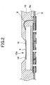
- FIG. 2 is a cross-sectional view of the fingerprint sensor apparatus, which is molded in a state where the seal resin enters between the sensor part 4 and the spacer 14. Opening 10a of the seal resin part 10 is formed in a part at which the spacer 14 was placed during the molding process, and the sensor part 4 is exposed within the opening 10a.
- the seal resin which entered between the sensor part 4 and the spacer 14 serves as a mold flash 16, and adheres to the surface of the sensor part 4. For this reason, a part of the surface of the sensor part 4 is covered by the mold flash 16, and such a part may lose the function as the sensor part. That is, the area of the part, which provides the functions as a sensor part 4, may be reduced.
- the fingerprint sensor is of a so-called area type in which the sensor part 4 has a relatively large area, the remaining uncovered part can maintain the function as the sensor part since a ratio of the part covered by the mold flash is small.
- a width H of the sensor part 4 is very as small as 1 mm.
- a length L of a mold flash is 0.3mm - 0.5mm, and a large part of the sensor part 4 may be covered by the mold flash, which results in fail in the function of the sensor part.
- a more specific object of the present invention is to provide a fingerprint sensor apparatus which can provide a normal fingerprint sensor function even when a mold flash is formed.
- Another object of the present invention is to provide a sweep-type fingerprint sensor which can provide an easy finger movement by reducing a resin part surrounding a sensor part.
- a fingerprint sensor apparatus for recognizing a pattern of a fingerprint by being contacted by a finger, comprising: a semiconductor chip having a surface on which a sensor part is formed; and a seal resin part which encapsulates the semiconductor chip, wherein the sensor part is exposed in a bottom of an opening formed in the seal resin part, and a distance between an edge of the bottom of the opening and an edge of the sensor part is 0.3 mm to 0.1 mm.
- the semiconductor chip when the semiconductor chip is resin-molded while the spacer is pressed against the sensor part so as to expose the sensor part, and if the resin enters between the sensor part and the semiconductor chip and a mold flash is formed, the mold flash does not reach the sensor part, which maintains a normal function of the sensor part.
- a fingerprint sensor apparatus for recognizing a pattern of a fingerprint by being contacted by a finger, comprising: a semiconductor chip having a surface on which a sensor part is formed; and a seal resin part which encapsulates the semiconductor chip, wherein the sensor part is exposed in a bottom of an opening formed in the seal resin part; the bottom of the opening has a step formed by a first surface and a second surface which is higher than the first surface, the sensor part being exposed on the first surface; and a distance between the first surface and the second surface in a direction perpendicular to a surface of the sensor part is 70 ⁇ m to 150 ⁇ m.
- the bottom of the opening has a two-stage structure, and the thickness of the portion of the seal resin part surrounding the sensor part is smaller than other portions.
- a resin-filling pressure is reduced when the seal resin is filled in a space corresponding to the portion having the reduced thickness, thereby preventing occurrence of a mold flash.
- a fingerprint sensor apparatus for recognizing a pattern of a fingerprint by being contacted by a finger, comprising: a semiconductor chip having a surface on which a sensor part is formed; and a seal resin part which encapsulates the semiconductor chip, wherein the sensor part and a part of a surface of the semiconductor chip are exposed in a bottom of an opening formed in the seal resin part, and a portion of the seal resin part forming the opening in a direction in which the finger is moved is a flat surface within the same plane in which an exposed surface of the semiconductor chip lies.
- a protrusion may be formed as a part of the seal resin part, the protrusion extending astride and along a boundary between the exposed surface of the semiconductor chip and the flat surface of the seal resin part. Accordingly, since the edge of the semiconductor chip is covered by the protrusion of the seal resin part, the edge of the semiconductor chip, which is easily chipped or cracked, is protected.
- a fingerprint sensor apparatus for recognizing a pattern of a fingerprint by being contacted by a finger, comprising: a semiconductor chip having a surface on which a sensor part is formed; and a seal resin part which encapsulates the semiconductor chip, wherein the sensor part and a part of a surface of the semiconductor chip are exposed in a bottom of an opening formed in the seal resin part, and a portion of the seal resin part forming the opening in a direction in which the finger is moved is lower than other portions of the seal resin part but higher than an exposed surface of the semiconductor chip.
- a manufacturing method of a fingerprint sensor apparatus for recognizing a pattern of a fingerprint by being contacted by a finger, comprising the steps of: attaching a spacer onto a predetermined position of a mold die for resin-molding a semiconductor chip having a surface on which a sensor part is formed, the spacer having a width greater than a width of the sensor part by a predetermined length; and placing the semiconductor chip inside the mold die, and resin-molding the semiconductor chip in a state where the spacer covers the sensor part of the semiconductor chip.
- the semiconductor chip when the semiconductor chip is resin-molded while the spacer is pressed against the sensor part so as to expose the sensor part, and if the resin enters between the sensor part and the semiconductor chip and a mold flash is formed, the mold flash does not reach the sensor part, which maintains a normal function of the sensor part.
- the spacer may cover an entire width of the sensor part, and a portion of the spacer extending beyond an edge of the sensor part may extend beyond an edge of a surface of the semiconductor chip. Accordingly, the upper surface of the semiconductor chip continuing from the sensor part is exposed. Thus, when the finger is moved (scanned) along the sensor part while the finger contacts the sensor part, a fingerprint recognition operation can be smoothly carried out, and an accurate recognition can be maintained.
- a manufacturing method of a fingerprint sensor apparatus for recognizing a pattern of a fingerprint by being contacted by a finger, comprising the steps of: applying a protective film having a predetermined thickness over a portion of a surface of a semiconductor chip and a sensor part formed on the surface of the semiconductor chip; placing the semiconductor chip inside the mold die, and resin-molding the semiconductor chip in a state where the protective tape covers the sensor part of the semiconductor chip; and removing the protective film from the semiconductor chip by pealing after the resin-molding so as to expose the sensor part and the portion of the surface of the semiconductor chip.
- the sensor part and the upper surface of the semiconductor chip can be easily exposed by merely resin-molding the semiconductor chip after applying the protective tape on the sensor part and the surrounding part.
- a manufacturing method of a fingerprint sensor apparatus for recognizing a pattern of a fingerprint by being contacted by a finger, comprising the steps of: forming a photosensitive resin film having a predetermined thickness over a portion of a surface of a semiconductor chip and a sensor part formed on the surface of the semiconductor chip; placing the semiconductor chip inside the mold die, and resin-molding the semiconductor chip in a state where the photosensitive resin film covers the sensor part of the semiconductor chip; and removing the protective film from the semiconductor chip by exposure after the resin-molding so as to expose the sensor part and the portion of the surface of the semiconductor chip.
- the sensor part and the upper surface of the semiconductor chip can be easily exposed by merely resin-molding the semiconductor chip after forming the photosensitive film on the sensor part and the surrounding part.
- the fingerprint sensor apparatus according to the first embodiment of the present invention differs from the fingerprint sensor shown in FIG. 2 with respect to the point of having an opening 18 larger than the opening 10a formed on the upper surface of the seal resin part 10 of the fingerprint sensor apparatus shown in FIG. 2.
- the basic structure of the fingerprint sensor apparatus shown in FIG. 3 is the same as the structure of the fingerprint sensor shown in FIG. 2, and the semiconductor chip 2 fixed by a die attachment material 22 onto a circuit board is molded by a seal resin.
- the opening 18 is formed in the seal resin part 10, and the sensor part 4 of the semiconductor chip 2 is exposed in the bottom of the opening 18.
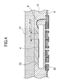
- FIG. 4 is a cross-sectional view showing a process of encapsulating the semiconductor chip 2 by the seal resin in a production process of the fingerprint sensor apparatus shown in FIG. 3.
- the opening 18 of the seal resin part 10 is formed by placing a spacer 20 inside a mold die.
- the fingerprint sensor apparatus according to the present embodiment has a flat configuration of 4.5 mm x 14 mm, and the semiconductor chip 2 has a flat configuration of 3 mm x 13 mm.
- the sensor part 4 is formed in an elongated area having a width of about 1 mm.
- the sensor part 4 shown in FIG. 3 and FIG. 4 is indicated by a cross section in a direction of a width of the sensor part 4.
- the spacer 20 is attached to the mold die 12 so that the spacer 20 is positioned between the mold die 12 and the sensor part 4.
- a part into which the seal resin does not flow due to the spacer 20 corresponds to the opening 18. That is, the seal resin part is removed from the mold die 12, the opening 18 is formed in the position where the spacer 20 was present, and the sensor part 4 is exposed in the bottom of the opening 18.
- the width of the semiconductor chip is about 4 mm, if the above-mentioned dimension S exceeds 1 mm, it will become impossible to carry out resin encapsulation of the electrodes of the semiconductor chip 2 formed on the same surface as the sensor part 4. It is preferable to set the above-mentioned distance S to 0.3 mm - 1.0 mm based on the above-mentioned restrictions on dimensions.
- a start point of the distance S is determined as a position corresponding to the end of the spacer 20, that is, an end of the bottom of the opening 18 when a mold flash is not formed.
- FIG. 5 is a cross-sectional view of a fingerprint sensor apparatus according to the second embodiment of the present invention.
- FIG. 6 is a cross-sectional view showing a process of resin-molding the semiconductor chip 2 in a production process of the fingerprint sensor apparatus shown in FIG. 5.
- the fingerprint sensor apparatus according to the second embodiment of the present invention has the same structure as the fingerprint sensor apparatus according to the first embodiment shown in FIG. 3 except for the configuration of the opening formed in the resin seal part.
- the configuration of the opening has a step in the bottom thereof as shown in FIG. 5 so that a step part 18A having a height of 70 micron to 150 micron is formed around the exposed surface of the sensor part 4.
- the spacer 20A is formed as a two-step configuration, as shown in FIG. 6. That is, the surface of the upper stage of the spacer 20A contacts the sensor part 4 and is pressed, and the surface around the upper stage is located 70 ⁇ m - 150 ⁇ m below the upper stage surface.
- the seal resin flows into a gap space G of 70 ⁇ m to 150 ⁇ m formed between the lower stage surface and the surface of the semiconductor chip 2, thereby forming the step part 18A as shown in FIG. 5.
- the seal resin cannot flow into the gap G.
- the height of step par is too large, a pressure loss is small and the seal resin maintains a pressure sufficient to form a mold flash. If the seal resin is that normally used for transfer molding and if the gap G is 70 ⁇ m to 150 ⁇ m, the seal resin can reach the deepest part of the gap while a pressure of the seal resin is decreased appropriately. Therefore, without producing a mould flash in the bottom of the opening 18 of the seal resin part 10, the entire surface of the semiconductor chip 2 can be encapsulated by the seal resin with the sensor part 4 being uncovered.
- the fingerprint sensor apparatus according to the third embodiment is particularly related to a sweep-type fingerprint sensor apparatus.
- the sweep-type fingerprint sensor apparatus is explained with reference to FIG. 7.
- the sweep-type fingerprint sensor apparatus is a sensor, which recognizes a pattern of a fingerprint by moving a finger having a fingerprint while contacting the finger with a sensor part.
- a capacitance sensor may be used as a sensor part, and, in such a case, an individual fingerprint pattern is recognized by carrying out an operation on a change in capacitance due to a movement of unevenness corresponding to the fingerprint when moving a finger. Therefore, if the height H of the part surrounding the opening in which the sensor part is exposed is large, it is difficult to move the finger while contacting a finger with the sensor part. For this reason, it is preferable that the surrounding part of the opening in the direction of movement of the finger is maintained as low as possible.
- FIG. 8 is a cross-sectional view of the fingerprint sensor apparatus according to the third embodiment of the present invention.
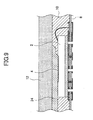
- FIG. 9 is a cross-sectional view showing a process of resin-molding the semiconductor chip 2 in a production process of the fingerprint sensor apparatus shown in FIG. 8.
- parts that are the same as the parts shown in FIG. 5 and FIG. 6 are give the same reference numerals, and descriptions thereof will be omitted.
- the semiconductor chip 2 is encapsulated by the seal resin in a state where the surface of the semiconductor chip 2 is exposed on a downstream side of the sensor part in the scanning direction. That is, the semiconductor chip 2 is encapsulated by the seal resin in a state where the seal resin in a surrounding part of the opening 18B on the downstream side of the sensor part 4 in the scanning direction is removed. It should be noted that a protective film is preferably formed on an exposed part of the upper surface of the semiconductor chip.
- the above-mentioned opening 18B can be formed by attaching a spacer 24 to the mold die 12, as shown in FIG. 9, so that the spacer 24 extends on the downstream side of the sensor part 4 in the scanning direction.
- the spacer 24 is configured and arranged to cover the upper surface of the semiconductor chip 2 to be encapsulated and extend further on the downstream side. Therefore, when scanning a finger for fingerprint recognition, the finger can be smoothly moved without any resistance, thereby improving an accuracy of fingerprint recognition.
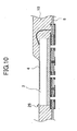
- FIG. 10 is a cross-sectional view showing a variation of the fingerprint sensor apparatus according to the above-mentioned third embodiment.
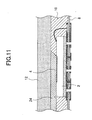
- FIG. 11 is a cross-sectional view showing a process of resin-molding the semiconductor chip in a production process of the fingerprint sensor apparatus shown in FIG. 10.
- the fingerprint sensor apparatus shown in FIG. 10 is provided with a protrusion 26 which is formed by the seal resin so as to slightly protrude along a boundary part between the semiconductor chip 10 and the seal resin part 10.
- the protrusion 26 can be easily formed by providing a notch in the spacer 24, the notch being configured to correspond to the configuration of the protrusion 26 as shown in FIG. 11.
- the protrusion 26 is provided at a location to cover the edge of the semiconductor chip 2, and serves to prevent the edge of the semiconductor chip 2 from being chipped or damaged.
- FIG. 12 is a cross-sectional view of the fingerprint sensor apparatus according to the fourth embodiment of the present invention.
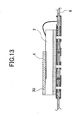
- FIG. 13 is a cross-sectional view showing a preparation process before carrying out resin-molding a semiconductor chip in a production process of the fingerprint sensor apparatus shown in FIG. 10.
- FIG. 14 is a cross-sectional view showing a process of resin-molding a semiconductor chip in a production process of the fingerprint sensor apparatus shown in FIG. 10.
- the fingerprint sensor apparatus has a structure in which a portion of the surface of the semiconductor chip 2 is exposed similar to the fingerprint sensor apparatus shown in FIG. 8 so that the sensor part 4 is easily scanned by a finger.
- the seal resin part 10 is formed slightly higher than the exposed surface of the semiconductor chip 2.
- a protective tape 30 is first applied onto the top surface of the semiconductor chip 2 before carrying out resin-molding.
- the protective tape 30 is preferably made of a material the same as that of the above-mentioned spacer. Then, as shown in FIG. 14, resin-molding is performed in a state where the protective tape 30 is applied over the sensor part 4 and a part of the surface of the semiconductor chip 2 that is to be exposed. After molding, the protective film 30 is removed by peeling, and the fingerprint sensor apparatus shown in FIG. 12 is completed. Therefore, a difference in height corresponding to the thickness of the protective tape 30 is generated between the top surface of the seal resin part 10 and the top surface of the semiconductor chip 2. Thereby, the edge of the semiconductor chip 2 can be protected.
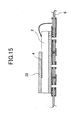
- a photosensitive resin may be applied over the sensor part 4 and the top surface of the semiconductor chip 2 instead of the protective tape 30. That is, as shown in FIG. 15, a photosensitive resin film 32 is formed on the sensor part 4 and the part of the surface of the semiconductor chip 2 that is to be exposed.
- the photosensitive resin film 32 can be formed using a technique to patternize and etch a resist, which is used in a conventional semiconductor chip manufacturing technique.
Landscapes
- Engineering & Computer Science (AREA)
- Human Computer Interaction (AREA)
- Physics & Mathematics (AREA)
- General Physics & Mathematics (AREA)
- Multimedia (AREA)
- Theoretical Computer Science (AREA)
- Measurement Of Length, Angles, Or The Like Using Electric Or Magnetic Means (AREA)
- Image Input (AREA)
- Measurement Of The Respiration, Hearing Ability, Form, And Blood Characteristics Of Living Organisms (AREA)
- Encapsulation Of And Coatings For Semiconductor Or Solid State Devices (AREA)
Abstract
Description
Claims (10)
- A fingerprint sensor apparatus for recognizing a pattern of a fingerprint by being contacted by a finger, comprising
a semiconductor chip having a surface on which a sensor part is formed; and
a seal resin part which encapsulates the semiconductor chip,
characterized in that:said sensor part is exposed in a bottom of an opening formed in the seal resin part, and a distance between an edge of the bottom of the opening and an edge of said sensor part is 0.3 mm to 0.1 mm. - A fingerprint sensor apparatus for recognizing a pattern of a fingerprint by being contacted by a finger, comprising:characterized in that:a semiconductor chip having a surface on which a sensor part is formed; anda seal resin part which encapsulates the semiconductor chip,said sensor part is exposed in a bottom of an opening formed in the seal resin part; the bottom of the opening has a step formed by a first surface and a second surface which is higher than the first surface, said sensor part being exposed on said first surface; and a distance between said first surface and said second surface in a direction perpendicular to a surface of the sensor part is 70 µm to 150 µm.
- A fingerprint sensor apparatus for recognizing a pattern of a fingerprint by being contacted by a finger, comprising:characterized in that said sensor part and a part of a surface of the semiconductor chip are exposed in a bottom of an opening formed in the seal resin part, and a portion of said seal resin part forming said opening in a direction in which the finger is moved is a flat surface within the same plane in which an exposed surface of said semiconductor chip lies.a semiconductor chip having a surface on which a sensor part is formed; anda seal resin part which encapsulates the semiconductor chip,
- The fingerprint sensor apparatus as claimed in claim 3, characterized in that a protrusion is formed as a part of said seal resin part, the protrusion extending astride and along a boundary between the exposed surface of said semiconductor chip and said flat surface of said seal resin part.
- A fingerprint sensor apparatus for recognizing a pattern of a fingerprint by being contacted by a finger, comprising:characterized in that said sensor part and a part of a surface of the semiconductor chip are exposed in a bottom of an opening formed in the seal resin part, and a portion of said seal resin part forming said opening in a direction in which the finger is moved is lower than other portions of the seal resin part but higher than an exposed surface of said semiconductor chip.a semiconductor chip having a surface on which a sensor part is formed; anda seal resin part which encapsulates the semiconductor chip,
- A manufacturing method of a fingerprint sensor apparatus for recognizing a pattern of a fingerprint by being contacted by a finger, characterized by the steps of:attaching a spacer onto a predetermined position of a mold die for resin-molding a semiconductor chip having a surface on which a sensor part is formed, the spacer having a width greater than a width of said sensor part by a predetermined length; andplacing said semiconductor chip inside the mold die, and resin-molding said semiconductor chip in a state where said spacer covers said sensor part of said semiconductor chip.
- The manufacturing method as claimed in claim 6, characterized in that said spacer covers an entire width of said sensor part, and a portion of said spacer extending beyond an edge of said sensor part in a direction of the width is 0.3 mm to 1.0 mm.
- The manufacturing method as claimed in claim 6, characterized in that said spacer covers an entire width of said sensor part, and a portion of said spacer extending beyond an edge of said sensor part extends beyond an edge of a surface of said semiconductor chip.
- A manufacturing method of a fingerprint sensor apparatus for recognizing a pattern of a fingerprint by being contacted by a finger, characterized by the steps of:applying a protective film having a predetermined thickness over a portion of a surface of a semiconductor chip and a sensor part formed on the surface of the semiconductor chip;placing said semiconductor chip inside said mold die, and resin-molding said semiconductor chip in a state where said protective tape covers the sensor part of said semiconductor chip; andremoving said protective film from said semiconductor chip by pealing after the resin-molding so as to expose said sensor part and said portion of the surface of said semiconductor chip.
- A manufacturing method of a fingerprint sensor apparatus for recognizing a pattern of a fingerprint by being contacted by a finger, characterized by the steps of:forming a photosensitive resin film having a predetermined thickness over a portion of a surface of a semiconductor chip and a sensor part formed on the surface of the semiconductor chip;placing said semiconductor chip inside said mold die, and resin-molding said semiconductor chip in a state where said photosensitive resin film covers the sensor part of said semiconductor chip; andremoving said protective film from said semiconductor chip by exposure after the resin-molding so as to expose said sensor part and said portion of the surface of said semiconductor chip.
Applications Claiming Priority (2)
| Application Number | Priority Date | Filing Date | Title |
|---|---|---|---|
| JP2002043708 | 2002-02-20 | ||
| JP2002043708A JP3766034B2 (en) | 2002-02-20 | 2002-02-20 | Fingerprint sensor device and manufacturing method thereof |
Publications (3)
| Publication Number | Publication Date |
|---|---|
| EP1339009A2 true EP1339009A2 (en) | 2003-08-27 |
| EP1339009A3 EP1339009A3 (en) | 2003-10-15 |
| EP1339009B1 EP1339009B1 (en) | 2005-12-28 |
Family
ID=27655269
Family Applications (1)
| Application Number | Title | Priority Date | Filing Date |
|---|---|---|---|
| EP02257538A Expired - Lifetime EP1339009B1 (en) | 2002-02-20 | 2002-10-30 | Fingerprint sensor apparatus |
Country Status (7)
| Country | Link |
|---|---|
| US (1) | US7192798B2 (en) |
| EP (1) | EP1339009B1 (en) |
| JP (1) | JP3766034B2 (en) |
| KR (2) | KR100833554B1 (en) |
| CN (1) | CN1202566C (en) |
| DE (1) | DE60208328T2 (en) |
| TW (1) | TWI222034B (en) |
Families Citing this family (45)
| Publication number | Priority date | Publication date | Assignee | Title |
|---|---|---|---|---|
| US6653723B2 (en) * | 2002-03-09 | 2003-11-25 | Fujitsu Limited | System for providing an open-cavity low profile encapsulated semiconductor package |
| FR2839570B1 (en) * | 2002-05-07 | 2004-09-17 | Atmel Grenoble Sa | METHOD OF MANUFACTURING FINGERPRINT SENSOR AND CORRESPONDING SENSOR |
| JP3614840B2 (en) * | 2002-11-28 | 2005-01-26 | 沖電気工業株式会社 | Semiconductor device |
| JP2006509371A (en) * | 2002-12-09 | 2006-03-16 | アドバンスド インターコネクト テクノロジーズ リミテッド | Package with exposed integrated circuit device |
| JP4241457B2 (en) * | 2003-06-26 | 2009-03-18 | 富士ゼロックス株式会社 | Manufacturing method of light emitting element with lens |
| US20050136851A1 (en) | 2003-12-19 | 2005-06-23 | Fujitsu Limited | Information processing unit |
| JP2005346271A (en) * | 2004-06-01 | 2005-12-15 | Fujitsu Ltd | Fingerprint sensor package |
| CN103559477B (en) * | 2004-11-03 | 2017-06-13 | 笔一公司 | For contact pilotage or the finger guide device of pen |
| JP4731191B2 (en) | 2005-03-28 | 2011-07-20 | 富士通セミコンダクター株式会社 | Semiconductor device and manufacturing method of semiconductor device |
| US7424136B2 (en) * | 2005-10-18 | 2008-09-09 | Authentec, Inc. | Finger sensing with enhanced mounting and associated methods |
| WO2007099594A1 (en) * | 2006-02-28 | 2007-09-07 | Fujitsu Limited | Finger print reading sensor unit |
| TWI313501B (en) * | 2006-03-22 | 2009-08-11 | Ind Tech Res Inst | A process for manufacture plastic package of mems devices and the structure for the same |
| JP4757071B2 (en) | 2006-03-27 | 2011-08-24 | 富士通株式会社 | Fingerprint authentication apparatus and information processing apparatus |
| US7632698B2 (en) * | 2006-05-16 | 2009-12-15 | Freescale Semiconductor, Inc. | Integrated circuit encapsulation and method therefor |
| KR100792670B1 (en) | 2006-06-13 | 2008-01-09 | 주식회사 애트랩 | Semiconductor device and contact sensor device |
| US7566966B2 (en) * | 2007-09-05 | 2009-07-28 | Stats Chippac Ltd. | Integrated circuit package-on-package system with anti-mold flash feature |
| US8183675B2 (en) * | 2007-11-29 | 2012-05-22 | Stats Chippac Ltd. | Integrated circuit package-on-package system with anti-mold flash feature |
| JP2009267272A (en) * | 2008-04-29 | 2009-11-12 | New Japan Radio Co Ltd | Semiconductor hollow package and method of manufacturing the same |
| TW200950017A (en) * | 2008-05-19 | 2009-12-01 | Lightuning Tech Inc | Sensing apparatus with packaging material as sensing protection layer and method of manufacturing the same |
| US7898072B2 (en) * | 2008-07-11 | 2011-03-01 | Stats Chippac Ltd. | Package stacking system with mold contamination prevention |
| JP2013156066A (en) * | 2012-01-27 | 2013-08-15 | Wacom Co Ltd | Electrical capacitance pressure sensing semiconductor device |
| JP5892595B2 (en) | 2012-02-06 | 2016-03-23 | 株式会社ワコム | Position indicator |
| US9030440B2 (en) | 2012-05-18 | 2015-05-12 | Apple Inc. | Capacitive sensor packaging |
| US8912051B1 (en) * | 2012-08-01 | 2014-12-16 | Amkor Technology, Inc. | Method for controlling molding compound geometry around a semiconductor die |
| CN204808363U (en) | 2012-11-20 | 2015-11-25 | 韩国科泰高科株式会社 | Fingerprint sensor module, portable electronic device with this |
| KR101453022B1 (en) * | 2012-11-20 | 2014-10-22 | 크루셜텍 (주) | Fingerprint sensor module, portable electronic device having the same, and manufacturing method thereof |
| JP5916637B2 (en) | 2013-01-11 | 2016-05-11 | 日立オートモティブシステムズ株式会社 | Flow sensor and manufacturing method thereof |
| KR101298636B1 (en) | 2013-07-05 | 2013-08-20 | (주)드림텍 | Method of manufacturing fingerprint recognition home key for strengthening adhesion and screening effect between sensing surface and coating layer and the fingerprint recognition home key structure thereof |
| US10296773B2 (en) | 2013-09-09 | 2019-05-21 | Apple Inc. | Capacitive sensing array having electrical isolation |
| US9697409B2 (en) * | 2013-09-10 | 2017-07-04 | Apple Inc. | Biometric sensor stack structure |
| US20150296622A1 (en) * | 2014-04-11 | 2015-10-15 | Apple Inc. | Flexible Printed Circuit With Semiconductor Strain Gauge |
| CN104051367A (en) * | 2014-07-01 | 2014-09-17 | 苏州晶方半导体科技股份有限公司 | Packaging structure and packaging method for fingerprint recognition chip |
| CN104538379A (en) * | 2014-12-31 | 2015-04-22 | 华天科技(西安)有限公司 | Fingerprint designing and packaging structure based on partial encapsulation technology and preparing method thereof |
| CN104851853A (en) * | 2015-05-19 | 2015-08-19 | 苏州晶方半导体科技股份有限公司 | Fingerprint identification chip packaging structure and packaging method |
| CN106767628B (en) * | 2015-12-18 | 2019-04-19 | 深圳市汇顶科技股份有限公司 | A kind of thickness detecting method and system of fingerprint sensor protective layer |
| JP6086166B1 (en) * | 2016-02-05 | 2017-03-01 | 第一精工株式会社 | Resin sealing mold, resin sealing device and resin sealing method |
| TWI575620B (en) * | 2016-03-10 | 2017-03-21 | 南茂科技股份有限公司 | Manufacturing method and manufacturing apparatus of fingerprint identification chip package structure |
| TWI614695B (en) * | 2017-07-03 | 2018-02-11 | 敦泰電子有限公司 | High screen ratio display device with fingerprint identification |
| CN110077657B (en) * | 2018-01-26 | 2021-03-09 | 致伸科技股份有限公司 | Fingerprint identification module packaging method |
| JP6784342B2 (en) | 2018-05-01 | 2020-11-11 | 株式会社村田製作所 | Electronic device and fingerprint authentication device equipped with it |
| CN109037169B (en) * | 2018-07-06 | 2020-10-23 | 昆山丘钛微电子科技有限公司 | Packaging mold, packaging structure, packaging method and camera module |
| CN113343829B (en) * | 2019-05-29 | 2024-04-09 | 深圳市汇顶科技股份有限公司 | Fingerprint recognition device and electronic device |
| KR102163694B1 (en) * | 2019-06-21 | 2020-10-08 | 시그네틱스 주식회사 | Fingerprint recognition sensor package |
| JP2022155336A (en) | 2021-03-30 | 2022-10-13 | ミツミ電機株式会社 | Detection device and manufacturing method thereof |
| KR20230056474A (en) | 2021-10-20 | 2023-04-27 | 삼성전자주식회사 | Fingerprint sensor package and Sensor package |
Family Cites Families (12)
| Publication number | Priority date | Publication date | Assignee | Title |
|---|---|---|---|---|
| DE3330975A1 (en) * | 1983-08-27 | 1985-03-21 | Licentia Patent-Verwaltungs-Gmbh, 6000 Frankfurt | Method and apparatus for encapsulating a semiconductor component |
| JPH04258176A (en) * | 1991-02-12 | 1992-09-14 | Mitsubishi Electric Corp | Semiconductor pressure sensor |
| KR960009089B1 (en) * | 1993-03-04 | 1996-07-10 | 문정환 | Mold for package molding and plastic charge-coupled device and the manufacturing method using the mold |
| KR970005706B1 (en) * | 1994-01-24 | 1997-04-19 | 금성일렉트론 주식회사 | Ccd and the manufacturing method |
| KR970005706A (en) * | 1995-07-19 | 1997-02-19 | 한승준 | Automotive air conditioner with blower to remove moisture remaining in evaporator |
| JP4024335B2 (en) * | 1996-01-26 | 2007-12-19 | ハリス コーポレイション | Integrated circuit device having an opening exposing die of integrated circuit and manufacturing method thereof |
| FR2749955B1 (en) * | 1996-06-14 | 1998-09-11 | Thomson Csf | FINGERPRINT READING SYSTEM |
| GB9725571D0 (en) * | 1997-12-04 | 1998-02-04 | Philips Electronics Nv | Electronic apparatus comprising fingerprint sensing devices |
| US6331452B1 (en) * | 1999-04-12 | 2001-12-18 | Verdicom, Inc. | Method of fabricating integrated circuit package with opening allowing access to die |
| US6603191B2 (en) * | 2000-05-18 | 2003-08-05 | Casio Computer Co., Ltd. | Semiconductor device and method of manufacturing the same |
| JP2003058872A (en) * | 2001-08-21 | 2003-02-28 | Sony Corp | Fingerprint detecting device, manufacturing method thereof and film forming device |
| US6815262B2 (en) * | 2002-07-22 | 2004-11-09 | Stmicroelectronics, Inc. | Apparatus and method for attaching an integrated circuit sensor to a substrate |
-
2002
- 2002-02-20 JP JP2002043708A patent/JP3766034B2/en not_active Expired - Fee Related
- 2002-10-30 DE DE60208328T patent/DE60208328T2/en not_active Expired - Lifetime
- 2002-10-30 EP EP02257538A patent/EP1339009B1/en not_active Expired - Lifetime
- 2002-11-05 TW TW091132592A patent/TWI222034B/en not_active IP Right Cessation
- 2002-11-07 US US10/289,268 patent/US7192798B2/en not_active Expired - Lifetime
- 2002-11-18 KR KR1020020071515A patent/KR100833554B1/en not_active Expired - Fee Related
- 2002-11-22 CN CNB021524076A patent/CN1202566C/en not_active Expired - Fee Related
-
2007
- 2007-12-05 KR KR1020070125516A patent/KR100805291B1/en not_active Expired - Fee Related
Also Published As
| Publication number | Publication date |
|---|---|
| US20030156743A1 (en) | 2003-08-21 |
| US7192798B2 (en) | 2007-03-20 |
| EP1339009B1 (en) | 2005-12-28 |
| TWI222034B (en) | 2004-10-11 |
| KR100833554B1 (en) | 2008-05-29 |
| CN1440060A (en) | 2003-09-03 |
| KR100805291B1 (en) | 2008-02-20 |
| CN1202566C (en) | 2005-05-18 |
| KR20070121623A (en) | 2007-12-27 |
| JP2003235830A (en) | 2003-08-26 |
| DE60208328D1 (en) | 2006-02-02 |
| TW200303491A (en) | 2003-09-01 |
| EP1339009A3 (en) | 2003-10-15 |
| KR20030069782A (en) | 2003-08-27 |
| DE60208328T2 (en) | 2006-07-20 |
| JP3766034B2 (en) | 2006-04-12 |
Similar Documents
| Publication | Publication Date | Title |
|---|---|---|
| US7192798B2 (en) | Fingerprint sensor apparatus and manufacturing method thereof | |
| JP5579420B2 (en) | Integrated lead frame and bezel structure and apparatus formed therefrom | |
| US8569875B2 (en) | Integrally molded die and bezel structure for fingerprint sensors and the like | |
| US6667439B2 (en) | Integrated circuit package including opening exposing portion of an IC | |
| US7049166B2 (en) | Methods and apparatus for making integrated circuit package including opening exposing portion of the IC | |
| EP0862211A2 (en) | Semiconductor apparatus and method for fabricating the same | |
| US20180061747A1 (en) | Package structure and method for fabricating the same | |
| US7393711B2 (en) | Method of producing a digital fingerprint sensor and the corresponding sensor | |
| JP2005528680A5 (en) | ||
| CN111554652B (en) | Conductive trace design for smart cards | |
| JP4441483B2 (en) | Fingerprint sensor device | |
| US11404361B2 (en) | Method for fabricating package structure having encapsulate sensing chip | |
| KR960000220B1 (en) | Chip-on-board semiconductor package and manufacturing method thereof | |
| KR980012306A (en) | A printed circuit board on which a resin dam is formed and a chip on board type semiconductor chip package |
Legal Events
| Date | Code | Title | Description |
|---|---|---|---|
| PUAI | Public reference made under article 153(3) epc to a published international application that has entered the european phase |
Free format text: ORIGINAL CODE: 0009012 |
|
| AK | Designated contracting states |
Designated state(s): AT BE BG CH CY CZ DE DK EE ES FI FR GB GR IE IT LI LU MC NL PT SE SK TR |
|
| AX | Request for extension of the european patent |
Extension state: AL LT LV MK RO SI |
|
| PUAL | Search report despatched |
Free format text: ORIGINAL CODE: 0009013 |
|
| RIC1 | Information provided on ipc code assigned before grant |
Ipc: 7H 01L 21/56 B Ipc: 7G 06K 9/00 A Ipc: 7H 01L 23/31 B |
|
| AK | Designated contracting states |
Kind code of ref document: A3 Designated state(s): AT BE BG CH CY CZ DE DK EE ES FI FR GB GR IE IT LI LU MC NL PT SE SK TR |
|
| AX | Request for extension of the european patent |
Extension state: AL LT LV MK RO SI |
|
| 17P | Request for examination filed |
Effective date: 20040204 |
|
| 17Q | First examination report despatched |
Effective date: 20040420 |
|
| AKX | Designation fees paid |
Designated state(s): DE FI FR GB |
|
| GRAP | Despatch of communication of intention to grant a patent |
Free format text: ORIGINAL CODE: EPIDOSNIGR1 |
|
| RTI1 | Title (correction) |
Free format text: FINGERPRINT SENSOR APPARATUS |
|
| GRAS | Grant fee paid |
Free format text: ORIGINAL CODE: EPIDOSNIGR3 |
|
| GRAA | (expected) grant |
Free format text: ORIGINAL CODE: 0009210 |
|
| AK | Designated contracting states |
Kind code of ref document: B1 Designated state(s): DE FI FR GB |
|
| REG | Reference to a national code |
Ref country code: GB Ref legal event code: FG4D |
|
| REF | Corresponds to: |
Ref document number: 60208328 Country of ref document: DE Date of ref document: 20060202 Kind code of ref document: P |
|
| ET | Fr: translation filed | ||
| PLBE | No opposition filed within time limit |
Free format text: ORIGINAL CODE: 0009261 |
|
| STAA | Information on the status of an ep patent application or granted ep patent |
Free format text: STATUS: NO OPPOSITION FILED WITHIN TIME LIMIT |
|
| 26N | No opposition filed |
Effective date: 20060929 |
|
| REG | Reference to a national code |
Ref country code: GB Ref legal event code: 732E |
|
| REG | Reference to a national code |
Ref country code: FR Ref legal event code: TP |
|
| REG | Reference to a national code |
Ref country code: FR Ref legal event code: CD Ref country code: FR Ref legal event code: CA |
|
| REG | Reference to a national code |
Ref country code: FR Ref legal event code: PLFP Year of fee payment: 15 |
|
| REG | Reference to a national code |
Ref country code: FR Ref legal event code: CA Effective date: 20170726 |
|
| REG | Reference to a national code |
Ref country code: FR Ref legal event code: PLFP Year of fee payment: 16 |
|
| REG | Reference to a national code |
Ref country code: FR Ref legal event code: PLFP Year of fee payment: 17 |
|
| PGFP | Annual fee paid to national office [announced via postgrant information from national office to epo] |
Ref country code: FR Payment date: 20190913 Year of fee payment: 18 |
|
| PGFP | Annual fee paid to national office [announced via postgrant information from national office to epo] |
Ref country code: DE Payment date: 20191015 Year of fee payment: 18 Ref country code: FI Payment date: 20191009 Year of fee payment: 18 |
|
| PGFP | Annual fee paid to national office [announced via postgrant information from national office to epo] |
Ref country code: GB Payment date: 20191031 Year of fee payment: 18 |
|
| REG | Reference to a national code |
Ref country code: DE Ref legal event code: R119 Ref document number: 60208328 Country of ref document: DE |
|
| REG | Reference to a national code |
Ref country code: FI Ref legal event code: MAE |
|
| GBPC | Gb: european patent ceased through non-payment of renewal fee |
Effective date: 20201030 |
|
| PG25 | Lapsed in a contracting state [announced via postgrant information from national office to epo] |
Ref country code: FR Free format text: LAPSE BECAUSE OF NON-PAYMENT OF DUE FEES Effective date: 20201031 Ref country code: FI Free format text: LAPSE BECAUSE OF NON-PAYMENT OF DUE FEES Effective date: 20201030 Ref country code: DE Free format text: LAPSE BECAUSE OF NON-PAYMENT OF DUE FEES Effective date: 20210501 |
|
| PG25 | Lapsed in a contracting state [announced via postgrant information from national office to epo] |
Ref country code: GB Free format text: LAPSE BECAUSE OF NON-PAYMENT OF DUE FEES Effective date: 20201030 |