EP1338904A1 - Light waveguide and its manufacturing method - Google Patents
Light waveguide and its manufacturing method Download PDFInfo
- Publication number
- EP1338904A1 EP1338904A1 EP01998169A EP01998169A EP1338904A1 EP 1338904 A1 EP1338904 A1 EP 1338904A1 EP 01998169 A EP01998169 A EP 01998169A EP 01998169 A EP01998169 A EP 01998169A EP 1338904 A1 EP1338904 A1 EP 1338904A1
- Authority
- EP
- European Patent Office
- Prior art keywords
- substrate
- optical
- waveguide
- refractive index
- groove
- Prior art date
- Legal status (The legal status is an assumption and is not a legal conclusion. Google has not performed a legal analysis and makes no representation as to the accuracy of the status listed.)
- Withdrawn
Links
Images


Classifications
-
- G—PHYSICS
- G02—OPTICS
- G02B—OPTICAL ELEMENTS, SYSTEMS OR APPARATUS
- G02B6/00—Light guides; Structural details of arrangements comprising light guides and other optical elements, e.g. couplings
- G02B6/10—Light guides; Structural details of arrangements comprising light guides and other optical elements, e.g. couplings of the optical waveguide type
- G02B6/12—Light guides; Structural details of arrangements comprising light guides and other optical elements, e.g. couplings of the optical waveguide type of the integrated circuit kind
- G02B6/122—Basic optical elements, e.g. light-guiding paths
- G02B6/1221—Basic optical elements, e.g. light-guiding paths made from organic materials
-
- G—PHYSICS
- G02—OPTICS
- G02B—OPTICAL ELEMENTS, SYSTEMS OR APPARATUS
- G02B6/00—Light guides; Structural details of arrangements comprising light guides and other optical elements, e.g. couplings
- G02B6/10—Light guides; Structural details of arrangements comprising light guides and other optical elements, e.g. couplings of the optical waveguide type
- G02B6/12—Light guides; Structural details of arrangements comprising light guides and other optical elements, e.g. couplings of the optical waveguide type of the integrated circuit kind
-
- G—PHYSICS
- G02—OPTICS
- G02B—OPTICAL ELEMENTS, SYSTEMS OR APPARATUS
- G02B6/00—Light guides; Structural details of arrangements comprising light guides and other optical elements, e.g. couplings
- G02B6/10—Light guides; Structural details of arrangements comprising light guides and other optical elements, e.g. couplings of the optical waveguide type
- G02B6/12—Light guides; Structural details of arrangements comprising light guides and other optical elements, e.g. couplings of the optical waveguide type of the integrated circuit kind
- G02B6/13—Integrated optical circuits characterised by the manufacturing method
- G02B6/132—Integrated optical circuits characterised by the manufacturing method by deposition of thin films
-
- G—PHYSICS
- G02—OPTICS
- G02B—OPTICAL ELEMENTS, SYSTEMS OR APPARATUS
- G02B6/00—Light guides; Structural details of arrangements comprising light guides and other optical elements, e.g. couplings
- G02B6/10—Light guides; Structural details of arrangements comprising light guides and other optical elements, e.g. couplings of the optical waveguide type
- G02B6/12—Light guides; Structural details of arrangements comprising light guides and other optical elements, e.g. couplings of the optical waveguide type of the integrated circuit kind
- G02B2006/12133—Functions
- G02B2006/12147—Coupler
Definitions
- the present invention relates to an optical waveguide mainly used for optical communication and a method of forming the same.
- An optical integrated circuit having various functions is actively studied in order to perform an advanced optical signal processing.
- An optical integrated circuit has an optical waveguide as a basic factor, which propagates light by covering a core region having a high refractive index with a clad layer having a relatively low refractive index and thereby confining the light in the core region and realizes various functions by pattering and arranging cores.
- a quartz-based optical waveguide has many advantages such as small loss, physical chemical stability, and adjustability with an optical fiber and serves as a typical passive optical waveguide.
- a typical optical-waveguide forming method uses the flame deposition method as a core-clad-film forming method and the reactive-ion etching method as a core-pattern forming method.
- the CVD method, vacuum deposition method, and sputtering method are proposed as core-clad forming methods in addition to the flame deposition method.
- a high-quality core can be formed by the flame deposition method or CVD method.
- the flame deposition method requires high-temperature annealing at 1,000°C or higher for more than ten hours a plurality of times and the CVD method has a difficult point in mass production that a film-forming area is narrow.
- the electron-beam deposition method or sputtering method can realize small-loss film formation, there is a problem in cost as an optical-waveguide forming process normally requiring a film thickness of ten to tens of microns because a film forming rate is low.
- FIGS. 5(a) to 5(c) show the above type of optical-waveguide forming method.
- a substrate 51 on which an optical-waveguide groove is formed is filled with a high-refractive-index material 52 used as a core.
- a clad substrate 53 and the optical-waveguide-groove substrate 51 are finally bonded together.
- the above optical waveguide has the following problems on cost and performance.
- the extra material when it is not completely removed, it remains as a waveguide layer. Particularly, when polishing, fine scratches are produced at a waveguide portion, and the scratches cause wave-guiding light to scatter. Therefore, the present situation has a problem in that an optical waveguide is not suitable for mass production and it is difficult to reduce the cost of the waveguide.
- a conventional optical waveguide has a problem that the waveguide is not suitable for mass production and it is difficult to reduce the cost of the waveguide.
- the present invention is made to solve the above problems of a conventional optical waveguide and its object is to provide an optical waveguide having high performance, mass productivity, and low cost and an optical-waveguide forming method.
- a first invention is an optical waveguide comprising:
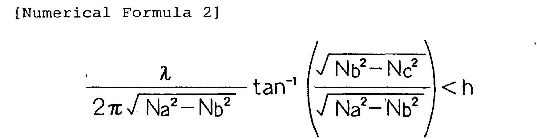
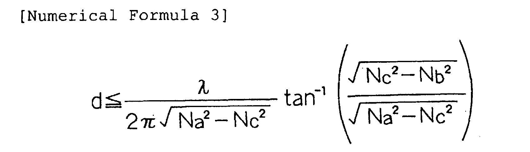
- a second invention of the present invention is the optical waveguide according to the first invention of the present invention, characterized in that by assuming the refractive index of said material as Na, that of said first substrate as Nb, that of said second substrate as Nc, the thickness of said material present between said second substrate and a portion other than said optical-waveguide groove on the plane on which the optical-waveguide groove of said first substrate is formed as d, the depth of said optical-waveguide groove as h, the wavelength of wave-guiding light as ⁇ ,
- a third invention of the present invention is the optical waveguide according to the first invention of the present invention, characterized in that an optical-waveguide groove is also formed on the plane of said second substrate bonded to said first substrate, and the optical waveguide of said second substrate is filled with said material.
- a fourth invention of the present invention is the optical waveguide according to the first invention of the present invention, characterized in that a third substrate bonded by said material is provided for the plane opposite to the plane of said second substrate bonded to said first substrate, an optical-waveguide groove is also formed on the plane of said third substrate bonded to said second substrate, the optical-waveguide groove of said third substrate is filled with said material, said material has a refractive index higher than that of said third substrate, and the refractive index of said second substrate is different from the refractive index of said third substrate.
- a fifth invention of the present invention is the optical waveguide according to any one of the first to the fourth inventions of the present invention, characterized in that said material is a glass-based material or resin.
- a sixth invention of the present invention is the optical waveguide according to the fifth invention of the present inveniton, characterized in that said material is a photo-curing resin, and the expression of bonding together by said material denotes bonding together by applying light to said photo-curing resin and curing the resin.
- a seventh invention of the present invention is the optical waveguide according to any one of the first to the fourth inventions of the present invention, characterized in that said substrate is formed by a glass-based material or a resin.
- An eighth invention of the present invention is the optical waveguide according to any one of the first to the fourth inventions of the present invention, characterized in that concave and convex portions of said optical-waveguide groove are collectively formed through molding by a mold material having concave and convex portions on its surface.
- a ninth invention of the present invention is an optical-waveguide forming method of forming an optical waveguide having at least a first substrate and a second substrate bonded to said first substrate, in which an optical-waveguide groove is formed on the bonded plane of at least either of said first and second substrates, comprising:
- a tenth invention of the present invention is an optical-waveguide forming method of forming an optical waveguide having at least a first substrate and a second substrate bonded to said first substrate, in which an optical-waveguide groove is formed on the bonded plane of at least either of said first and second substrates, comprising:
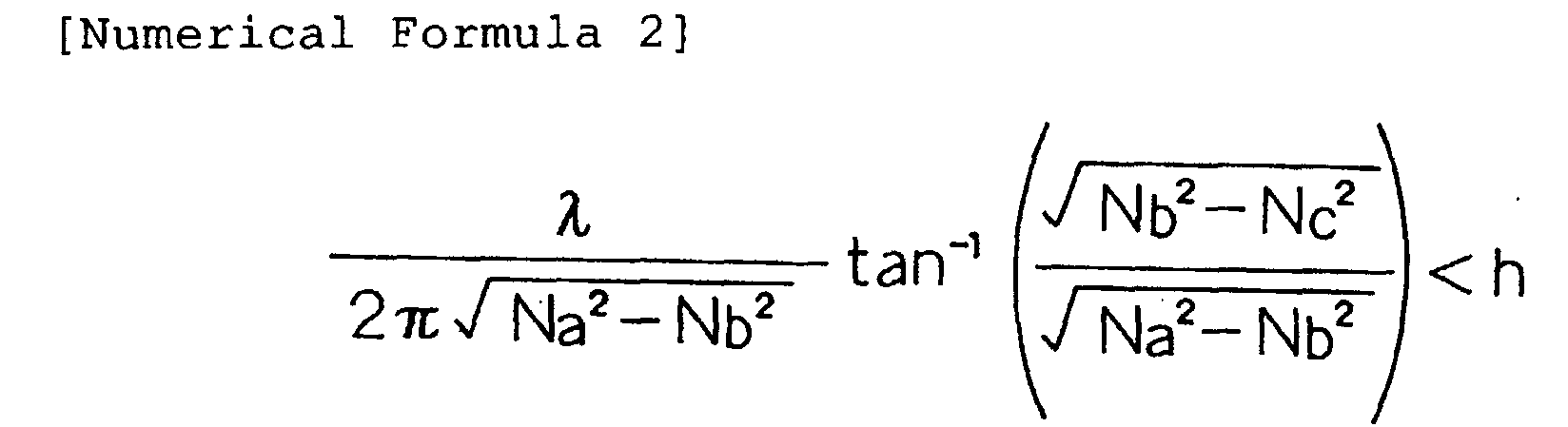
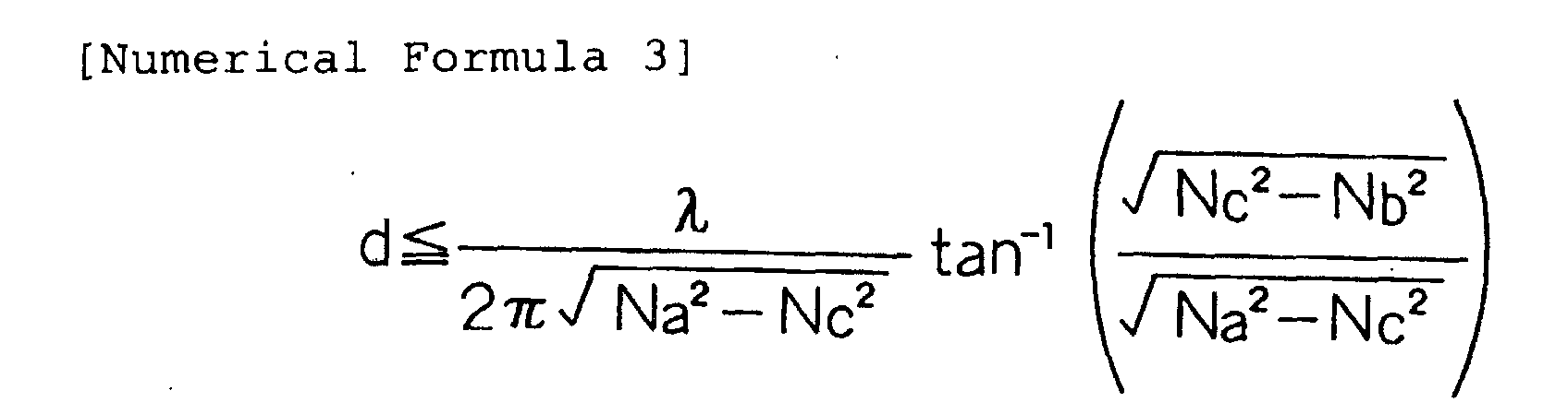
- An eleventh invention of the present invention is the optical-waveguide forming method according to the ninth or the tenth invention of the present invention, characterized in that by assuming the refractive index of said material as Na, that of said first substrate as Nb, that of said second substrate as Nc, the thickness of said material present between said second substrate and a portion other than said optical-waveguide groove on the plane on which the optical-waveguide groove of said first substrate is formed as d, the depth of said optical-waveguide groove as h, the wavelength of wave-guiding light as ⁇ ,
- a twelfth invention of the present invention (corresponding to Claim 12) is the optical-waveguide forming method according to the tenth invention of the present invention, characterized in that when making the refractive index of said first substrate different from the refractive index of said second substrate, even the other-hand substrate is heated at a temperature different from the case of one-hand substrate to change refractive indexes.
- a thirteenth invention of the present invention is the optical-waveguide forming method according to the tenth invention of the present invention), characterized in that when making the refractive index of said first substrate different from the refractive index of said second substrate, not only one-hand substrate but also the other-hand substrate are heated and cooled for periods different from each other to change refractive indexes.
- a fourteenth invention of the present invention is the optical-waveguide forming method according to the ninth or the tenth invention of the present invention, characterized in that at least either of said first and second substrates is heated and softened to form said optical-waveguide groove by pressing a mold material having concave and convex portions on the surface against the substrate.
- FIG. 1 shows the optical waveguide of the first embodiment of the present invention.
- an optical-waveguide groove is formed on the surface of the substrate 11 made of glass or transparent resin through molding using a mold (not illustrated) as shown in FIG. 1.
- an ultraviolet-curing resin is applied to an optical-waveguide-groove forming plane as the high-refractive-index material 12 and filled into a groove. Then, the optical-waveguide-groove substrate 11 and the clad substrate 13 having a refractive index different from that of the substrate 11 are bonded together .
- the ultraviolet-curing resin is applied by means of spin coating at a revolving speed of 500 to 7,000 rpm.
- the ultraviolet-curing resin in the groove is cured through irradiation with ultraviolet radiation.
- the ultraviolet-curing resin in the groove functions as an optical-waveguide core.
- the thickness of the adhesive layer is approx. 1 ⁇ m.
- FIGS. 2(a) to 2(c) show effects obtained by changing refractive indexes of the clad substrate 13 and optical-waveguide-groove substrate 11 by using a result of simulation.
- the axis of abscissa shows a thickness of an adhesive layer and the axis of ordinate shows an effective refractive index, and a point at which the continuous line of a graph intersects with the axis of abscissa shows a cutoff film thickness.
- a wavelength is set to 1.3 ⁇ m in every calculation.
- FIG. 2(a) shows a result of performing calculation by assuming the refractive index of a waveguide core as 1.453, that of the clad substrate 13 as 1.45, and that of the optical-waveguide-groove 11 as 1.45 equal to the refractive index of the clad substrate 13.
- the continuous line intersects at the origin, a wave-guiding mode is present even if an adhesive layer is made thin and light propagates through the adhesive layer.
- a cutoff film thickness becomes 1.8 ⁇ m as shown in FIG. 2(b) and thus, no wave is guided as long as the thickness is 1.8 ⁇ m or less even if an adhesive layer is present.
- a cutoff film thickness becomes 1.2 ⁇ m as shown in FIG. 2 (c) and no wave is guided as long as the thickness is 1.2 ⁇ m or less even if an adhesive layer is present similarly to the case of increasing the refractive index of the clad substrate 13.
- the refractive index of the optical-waveguide-groove substrate 11 is assumed as Nb
- the depth of the optical-waveguide groove formed on the optical-waveguide-groove substrate 11 is assumed as h
- the refractive index of the high-refractive-index material 12 is assumed as Na
- the refractive index of the clad substrate 13 is assumed as Nc.
- the thickness of an adhesive layer is assumed as d and the wavelength of wave-guiding light is assumed as ⁇ .
- wave-guiding light does not leak to the adhesive layer even if the thickness d of the adhesive layer is larger than zero.
- FIG. 8 shows a relation between adhesive-layer thickness and effective refractive index when h is 8 ⁇ m, ⁇ is 1.3 ⁇ m, Na is 1.507, Nb is 1.504, and Nc is 1.504. In this case, because a continuous line intersects at the origin, a wave-guiding mode is present even if the adhesive layer is made thin and light propagates through the adhesive layer.
- FIG. 9(a) shows a relation between adhesive-layer thickness and effective refractive index when increasing Nc by 0.001. That is, FIG. 9(a) shows a relation between adhesive-layer thickness and effective refractive index when h is 8 ⁇ m, ⁇ is 1.3 ⁇ m, Na is 1.507, Nb is 1.504, and Nc is 1.505.
- the cutoff film thickness becomes 1.8 ⁇ m , and no wave is guided when a cutoff film thickness is 1.8 ⁇ m or less even if an adhesive layer is present.
- FIG. 9(b) shows a case in which Nc is further increased by 0.001 from the case of Fig. 9(a). That is, FIG. 9(b) shows a relation between adhesive-layer thickness and effective refractive index when h is 8 ⁇ m, ⁇ is 1.3 ⁇ m, Na is 1.507, Nb is 1.504, and Nc is 1.506.
- a cutoff film thickness becomes 3.8 ⁇ m but no wave is guided when the thickness is 3.8 ⁇ m or less even if an adhesive layer is present. That is, when Nb is larger than Nc, wave-guiding light does not propagate through the adhesive layer even if the adhesive layer becomes thicker if the difference between refractive indexes of Nc and Nb increases.
- FIG. 10(a) shows a relation between adhesive-layer pressure and effective refractive index when decreasing Nc by 0.001 compared to the case of FIG. 8. That is, FIG. 10(a) shows a relation between adhesive-layer thickness and effective refractive index when h is 8 ⁇ m, ⁇ is 1.3 ⁇ m, Na is 1.507, Nb is 1.504, and Nc is 1.503.
- the cutoff film thickness becomes 1.3 ⁇ m and no wave is guided when the thickness is 1.3 ⁇ m or less even if the adhesive layer is present.
- FIG. 10(b) shows a case in which Nc is decreased by 0.001 from the case of FIG. 10(a). That is, FIG. 10(b) shows a relation between adhesive-layer thickness and effective refractive index when h is 8 ⁇ m, ⁇ is 1.3 ⁇ m, Na is 1.507, Nb is 1.504, and Nc is 1.502.
- the cutoff film thickness becomes 1.6 ⁇ m and no wave is guided when a cutoff film thickness is 1.6 ⁇ m or less even if an adhesive layer is present.
- the optical-waveguide-groove substrate 11 of this embodiment serves as a first substrate of the present invention and the clad substrate 13 of this embodiment serves as a second substrate of the present invention.
- the second substrate of the present invention is not restricted to a substrate of changing the refractive index of the clad substrate 13 as shown in this embodiment. In short, it is only necessary that the second substrate of the present invention is different from the first substrate of the present invention in refractive index such as a substrate changing the refractive index of the optical-waveguide-groove substrate 11.
- a refractive-index change is calculated as 0.001 in the case of this embodiment, the change is not restricted to 0.001. It is allowed to change a refractive index as long as refractive indexes of the clad substrate 13 and optical-waveguide-groove substrate 11 do not exceed the refractive index of a core.
- wavelength is calculated as 1.3 ⁇ m in the case of this embodiment, the wavelength is not restricted to 1.3 ⁇ m. Other wavelengths are also considered by generalizing them.
- an ultraviolet-curing resin is used as an optical-waveguide core material in the case of this embodiment
- the core material is not restricted to the resin. It is also allowed to use a thermosetting resin or glass-based material.
- spin coating is used as a method of coating a high-refractive-index material in the case of this embodiment, the coating method is not restricted to the spin coating. It is allowed to use dip coating or spray coating.
- an optical waveguide groove through molding as described for this embodiment from the viewpoint of productivity, formation of the groove is not restricted to molding. It is allowed to form the groove through etching according to necessity.
- linear waveguide is described as an example, this embodiment, is not restricted to the linear waveguide. It is possible to apply this embodiment to every optical waveguide pattern generally used and moreover control bend, branch, and combination of optical waves.
- optical-waveguide forming method of the second embodiment of the present invention is described below.
- FIGS. 6(a) to 6(d) show the optical-waveguide forming method of this embodiment.
- an optical-waveguide groove is formed on the surface of a substrate 11 made of glass or transparent resin through molding using a mold (not illustrated). That is, the optical-waveguide groove is formed by heating and thereby softening the substrate 11 and pressing a mold material having concave and convex portions on its surface against the substrate 11.
- ultraviolet radiation is applied to the substrate 11 on whitch an optical-waveguide groove is formed.
- a refractive-index change is induced due to a photochemical reaction. Therefore, it is possible to make the refractive index of the optical-waveguide-groove substrate 11 different from that of a clad substrate 13 even if using the same material for the substrates 11 and 13.
- a high-refractive-index material 12 is applied to an optical-waveguide-groove forming plane to fill a groove with the material 12 as shown in FIG. 6(c).
- the optical-waveguide-groove substrate 11 irradiated with ultraviolet radiation and the clad substrate 13 not irradiated with ultraviolet radiation are bonded together.
- a first substrate of the present invention is not restricted to the substrate of this embodiment changing the refractive index of the substrate 11 on which an optical-waveguide groove is formed like the case of this embodiment.
- changing the refractive index of the clad substrate 13 it is only necessary that the first substrate of the present invention is different from a second substrate of the present invention in refractive index.
- the first substrate of the present invention is not restricted to a substrate changing the refractive index of only the substrate 11 on which an optical waveguide groove is formed like the case of this embodiment.
- irradiating the clad substrate 13 and optical-waveguide-groove substrate 11 with ultraviolet radiation by different amount of irradiation it is only necessary that the first substrate of the present invention is different from the second substrate of the present invention in refractive index.
- optical-waveguide forming method of forming the optical waveguide shown in FIG. 1 is described for this embodiment.
- this embodiment is not restricted to the above method.
- the optical-waveguide forming method of this embodiment makes it possible to form the optical waveguide shown in FIG. 3 or 4.
- the optical waveguides shown in FIGS. 3 and 4 will be described later.
- an optical-waveguide groove forming method is not restricted to molding. However, it is also allowed to form an optical-waveguide groove through etching according to necessity.
- the substrate 11 is irradiated with ultraviolet radiation in the step shown in FIG. 6(b).
- a substrate 11 is heated and cooled instead.
- an optical waveguide groove is formed on the surface of the substrate 11 made of glass or transparent resin through molding using a mold (not illustrated) as shown in FIG. 1 similarly to the case of FIG. 6(a) of the second embodiment.
- the substrate 11 with the optical waveguide groove formed is heated.
- Glass has a structure corresponding to its heat history and the density of the glass at room temperature depends on a heating temperature or cooling rate.
- rapidly-cooled glass has a volume larger than slowly-cooled glass. Therefore, the refractive index of the former is different from that of the latter depending on a heating temperature or cooling rate. Therefore, it is possible to make the refractive index of the optical-waveguide-groove substrate 11 different from that of a clad substrate 13 even if using the same material for the both substrates 11 and 13.
- an ultraviolet-curing resin is applied to an optical-waveguide-groove forming plane as a high-refractive-index material 12 to fill a groove with the resin.
- the optical-waveguide-groove substrate 11 and the clad substrate 13 are bonded together.
- the ultraviolet-curing resin in the groove is cured.
- the ultraviolet-curing resin in the groove functions as an optical-waveguide core.
- refractive indexes are changed by heating a substrate with an optical waveguide groove formed. It is only necessary that the clad substrate 13 is different from the optical-waveguide-groove substrate 11 in refractive index, and it is allowed to change the refractive index of the clad substrate 13.
- refractive indexes are changed by heating only the substrate 11 with the optical-waveguide groove formed in the case of this embodiment, it is also allowed to heat two substrates at different temperatures.
- refractive indexes are changed by heating only the substrate 11 with the optical-waveguide groove formed in the case of this embodiment, it is also allowed to heat two substrates at the same temperature and cool them by changing cooling rates.
- an ultraviolet-curing resin is used as an optical-waveguide core material in the case of this embodiment
- the optical-waveguide core material is not restricted to the resin. It is allowed to use a glass-based material.
- an optical-waveguide-groove forming method is not restricted to molding. It is also allowed to form the optical-waveguide groove through etching according to necessity.
- FIG. 3 is an illustration showing an optical waveguide of the fourth embodiment of the present invention.
- an optical-waveguide groove is formed on the surface of a first substrate 31 made of glass or transparent resin through molding using a mold (not illustrated). Moreover, an optical-waveguide groove is formed on the surface of a second substrate 33 different from the first substrate 31 in refractive index through molding using a mold (not illustrated).
- an ultraviolet-curing resin is applied to an optical-waveguide-groove forming plane as a high-refractive-index material 32 to fill a groove with the resin.
- the first substrate 31 and the second substrate 33 are bonded together.
- the ultraviolet-curing resin in the groove is cured.
- the ultraviolet-curing resin in the groove functions as an optical-waveguide core.
- the first optical-waveguide-groove substrate 31 of this embodiment serves as a first substrate of the present invention and the second optical-waveguide-groove substrate 33 of this embodiment serves as a second substrate of the present invention.
- this embodiment uses a substrate having a refractive index different from that of the first substrate as the second substrate, it is also allowed to form a groove by using the same substrate and then change refractive indexes through heat treatment or irradiation with light.
- this embodiment uses an ultraviolet-curing resin as an optical-waveguide core material
- the core material is not restricted to the resin. It is also allowed to use a thermosetting resin or glass-based material.
- an optical-waveguide groove through molding as described for this embodiment.
- a method of forming the optical-waveguide groove is not restricted to molding. It is allowed to form the groove through etching according to necessity.
- the number of waveguides is not restricted to a pair of waveguides. It is also allowed to form a plurality of waveguides on one substrate.
- linear waveguide is described for this embodiment as an example, this embodiment is not restricted to the linear waveguide. It is possible to apply this embodiment to every optical-waveguide pattern generally used and moreover control bend, branch, and combination of optical waves.
- FIG. 4 is an optical waveguide of the fourth embodiment of the present invention.
- an optical-waveguide groove is formed on the surface of a first substrate 41 made of glass or transparent resin through molding using a mold (not illustrated). Moreover, an optical-waveguide groove is formed on surfaces of a first substrate 41 and a second substrate 43 through molding using a mold (not illustrated).
- an ultraviolet-curing resin is applied to an optical-waveguide-groove forming plane as a high-refractive-index material 42 to fill a groove with the resin.
- the first optical-waveguide-groove substrate 41 and second optical-waveguide-groove substrate 43 are bonded together through a clad substrate 44 different from the first optical-waveguide-groove substrate 41 and second optical-waveguide-groove substrate 43 in refractive index so that the optical-waveguide grooves are faced each other.
- the ultraviolet-curing resin in the groove is cured.
- the ultraviolet-curing resin in the groove functions as an optical-waveguide core.
- the first optical-waveguide-groove substrate 41 of this embodiment serves as a first substrate of the present invention
- the second optical-waveguide-groove substrate 43 of this embodiment serves as a third substrate of the present invention
- the clad substrate 44 of this embodiment serves as a second substrate of the present invention.
- this embodiment uses an ultraviolet-curing resin as an optical-waveguide core material
- the core material is not restricted to the ultraviolet-curing resin. It is allowed to use a thermosetting resin or glass-based material.
- an optical waveguide groove through molding as described for this embodiment from the viewpoint of productivity.
- a method of forming the groove is not restricted to molding. It is allowed to form the groove through etching according to necessity.
- this embodiment uses a substrate having a refractive index different from those of the first and second substrates as a clad substrate .
- it is also allowed to use the same substrate by changing refractive indexes through a heat treatment or irradiation with light.
- this embodiment is described by using a pair of waveguides as an example, it is allowed to form a plurality of waveguides on one substrate instead of the above mentioned.
- this embodiment is described by using a linear waveguide as an example , it is not restricted to the linear waveguide. It is possible to apply this embodiment to every optical waveguide pattern and moreover control bend, branch, and combination of optical waves.
- the present invention provides an optical waveguide which can be mass-produced at a low cost and an optical-waveguide forming method.
Landscapes
- Physics & Mathematics (AREA)
- Engineering & Computer Science (AREA)
- Microelectronics & Electronic Packaging (AREA)
- General Physics & Mathematics (AREA)
- Optics & Photonics (AREA)
- Optical Integrated Circuits (AREA)
Abstract
Description
by assuming the refractive index of said material as Na, that of said first substrate as Nb, that of said second substrate as Nc, the thickness of said material present between said second substrate and a portion other than said optical-waveguide groove on the plane on which the optical-waveguide groove of said first substrate is formed as d, the depth of said optical-waveguide groove as h, the wavelength of wave-guiding light as λ,


an optical-waveguide groove is also formed on the plane of said second substrate bonded to said first substrate, and
the optical waveguide of said second substrate is filled with said material.
a third substrate bonded by said material is provided for the plane opposite to the plane of said second substrate bonded to said first substrate,
an optical-waveguide groove is also formed on the plane of said third substrate bonded to said second substrate,
the optical-waveguide groove of said third substrate is filled with said material,
said material has a refractive index higher than that of said third substrate, and
the refractive index of said second substrate is different from the refractive index of said third substrate.
said material is a glass-based material or resin.
said material is a photo-curing resin, and
the expression of bonding together by said material denotes bonding together by applying light to said photo-curing resin and curing the resin.
said substrate is formed by a glass-based material or a resin.
concave and convex portions of said optical-waveguide groove are collectively formed through molding by a mold material having concave and convex portions on its surface.
by assuming the refractive index of said material as Na, that of said first substrate as Nb, that of said second substrate as Nc, the thickness of said material present between said second substrate and a portion other than said optical-waveguide groove on the plane on which the optical-waveguide groove of said first substrate is formed as d, the depth of said optical-waveguide groove as h, the wavelength of wave-guiding light as λ,

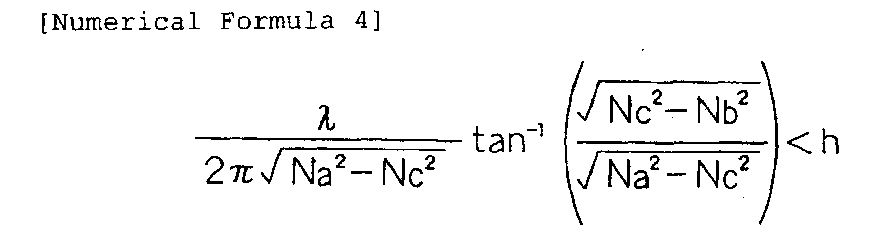
when making the refractive index of said first substrate different from the refractive index of said second substrate,
even the other-hand substrate is heated at a temperature different from the case of one-hand substrate to change refractive indexes.
when making the refractive index of said first substrate different from the refractive index of said second substrate,
not only one-hand substrate but also the other-hand substrate are heated and cooled for periods different from each other to change refractive indexes.
at least either of said first and second substrates is heated and softened to form said optical-waveguide groove by pressing a mold material having concave and convex portions on the surface against the substrate.
- 11, 51
- Optical-waveguide-groove substrate
- 31, 41
- First optical-waveguide-groove substrate
- 12, 32, 42, 52
- High-refractive-index material
- 13, 33, 44, 53
- Clad substrate
- 33, 43
- Second optical waveguide substrate



Claims (14)
- An optical waveguide comprising:a first substrate on which an optical-waveguide groove is formed and a second substrate, characterized in thatsaid second substrate is bonded to a plane of said first substrate on which said optical-waveguide groove is formed by a material having a refractive index higher than those of said first and second substrates,said optical-waveguide groove is filled with said material, andthe refractive index of said first substrate is different from that of said second substrate.
- The optical waveguide according to claim 1,
characterized in that
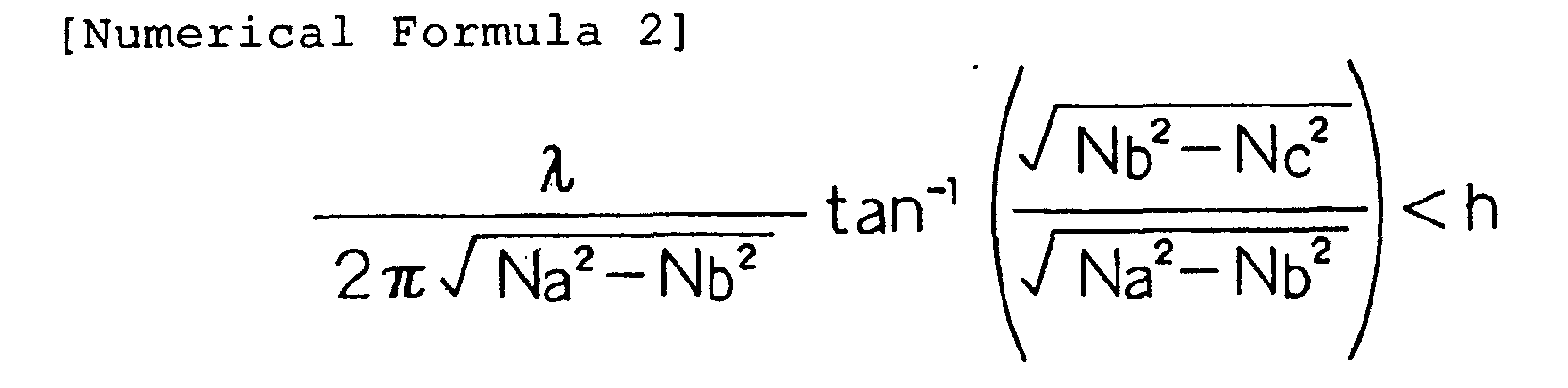
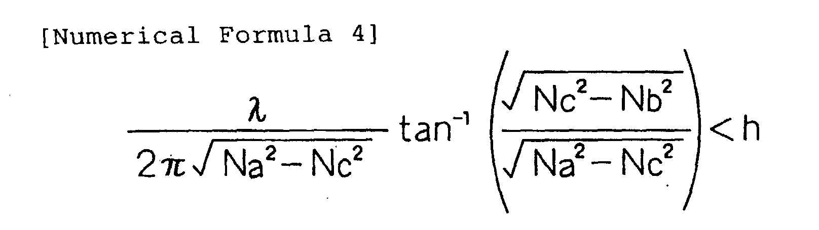
by assuming the refractive index of said material as Na, that of said first substrate as Nb, that of said second substrate as Nc, the thickness of said material present between said second substrate and a portion other than said optical-waveguide groove on the plane on which the optical-waveguide groove of said first substrate is formed as d, the depth of said optical-waveguide groove as h, the wavelength of wave-guiding light as λ,(1) when said Nb is not smaller than said Nc, said Na, Nb, Nc, d, h, and λ simultaneously satisfy the following numerical formulas, and
and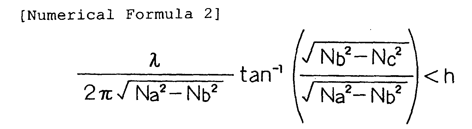 (2) when said Nb is smaller than said Nc, said Na, Nb, Nc, d, h, and λ simultaneously satisfy the following numerical formulas.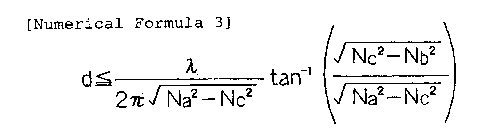
- The optical waveguide according to claim 1,
characterized in that
an optical-waveguide groove is also formed on the plane of said second substrate bonded to said first substrate, and
the optical waveguide of said second substrate is filled with said material. - The optical waveguide according to claim 1,
characterized in that
a third substrate bonded by said material is provided for the plane opposite to the plane of said second substrate bonded to said first substrate,
an optical-waveguide groove is also formed on the plane of said third substrate bonded to said second substrate,
the optical-waveguide groove of said third substrate is filled with said material,
said material has a refractive index higher than that of said third substrate, and
the refractive index of said second substrate is different from the refractive index of said third substrate. - The optical waveguide according to any one of claims 1 to 4, characterized in that
said material is a glass-based material or resin. - The optical waveguide according to claim 5,
characterized in that
said material is a photo-curing resin, and
the expression of bonding together by said material denotes bonding together by applying light to said photo-curing resin and curing the resin. - The optical waveguide according to any one of claims 1 to 4, characterized in that
said substrate is formed by a glass-based material or a resin. - The optical waveguide according to any one of claims 1 to 4, characterized in that
concave and convex portions of said optical-waveguide groove are collectively formed through molding by a mold material having concave and convex portions on its surface. - An optical-waveguide forming method of forming an optical waveguide having at least a first substrate and a second substrate bonded to said first substrate, in which an optical-waveguide groove is formed on the bonded plane of at least either of said first and second substrates, comprising:a step of making the refractive index of said first substrate different from the refractive index of said second substrate by applying light to at least either of said first and second substrates and thereby changing refractive indexes; anda step of bonding said first and second substrates different from each other in refractive index together by a material having a refractive index higher than refractive indexes of said first and second substrates.
- An optical-waveguide forming method of forming an optical waveguide having at least a first substrate and a second substrate bonded to said first substrate, in which an optical-waveguide groove is formed on the bonded plane of at least either of said first and second substrates, comprising:a step of making the refractive index of said first substrate different from the refractive index of said second substrate by heating and cooling at least either of said first or second substrates and thereby changing refractive indexes, anda step of bonding said first and second substrates whose refractive indexes are made different from each other by a material having a refractive index higher than those of said first and second substrates.
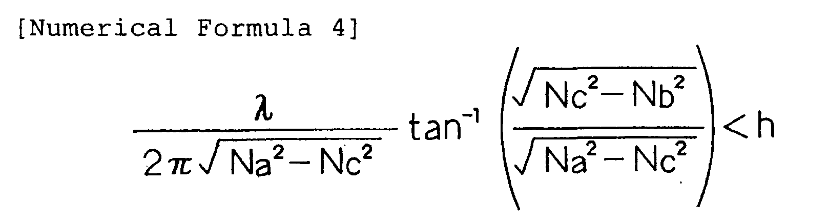
- The optical-waveguide forming method according to claim 9 or 10, characterized in that by assuming the refractive index of said material as Na, that of said first substrate as Nb, that of said second substrate as Nc, the thickness of said material present between said second substrate and a portion other than said optical-waveguide groove on the plane on which the optical-waveguide groove of said first substrate is formed as d, the depth of said optical-waveguide groove as h, the wavelength of wave-guiding light as λ,(1) when said Nb is not smaller than said Nc, said Na, Nb, Nc, d, h, and λ simultaneously satisfy the following numerical formulas,
 and
and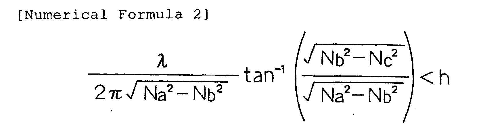 (2) when said Nb is smaller than said Nc, said Na, Nb, Nc, d, h, and λ simultaneously satisfy the following numerical formulas.
- The optical-waveguide forming method according to claim 10, characterized in that
when making the refractive index of said first substrate different from the refractive index of said second substrate,
even the other-hand substrate is heated at a temperature different from the case of one-hand substrate to change refractive indexes. - The optical-waveguide forming method according to claim 10, characterized in that
when making the refractive index of said first substrate different from the refractive index of said second substrate,
not only one-hand substrate but also the other-hand substrate are heated and cooled for periods different from each other to change refractive indexes. - The optical-waveguide forming method according to claim 9 or 10, characterized in that
at least either of said first and second substrates is heated and softened to form said optical-waveguide groove by pressing a mold material having concave and convex portions on the surface against the substrate.
Applications Claiming Priority (3)
| Application Number | Priority Date | Filing Date | Title |
|---|---|---|---|
| JP2000364173 | 2000-11-30 | ||
| JP2000364173 | 2000-11-30 | ||
| PCT/JP2001/010304 WO2002044776A1 (en) | 2000-11-30 | 2001-11-27 | Light waveguide and its manufacturing method |
Publications (2)
| Publication Number | Publication Date |
|---|---|
| EP1338904A1 true EP1338904A1 (en) | 2003-08-27 |
| EP1338904A4 EP1338904A4 (en) | 2005-08-24 |
Family
ID=18835162
Family Applications (1)
| Application Number | Title | Priority Date | Filing Date |
|---|---|---|---|
| EP01998169A Withdrawn EP1338904A4 (en) | 2000-11-30 | 2001-11-27 | LIGHT WAVE GUIDE AND METHOD OF MANUFACTURE |
Country Status (3)
| Country | Link |
|---|---|
| US (1) | US7024087B2 (en) |
| EP (1) | EP1338904A4 (en) |
| WO (1) | WO2002044776A1 (en) |
Cited By (3)
| Publication number | Priority date | Publication date | Assignee | Title |
|---|---|---|---|---|
| EP2023173A1 (en) * | 2007-08-06 | 2009-02-11 | Nitto Denko Corporation | Optical Waveguide Film and Manufacturing Method Thereof |
| US7822308B2 (en) | 2007-07-31 | 2010-10-26 | Nitto Denko Corporation | Optical waveguide film, optical substrate, and methods for manufacturing the same |
| CN103454722A (en) * | 2012-06-01 | 2013-12-18 | 鸿富锦精密工业(深圳)有限公司 | Optical waveguide and method for manufacturing same |
Families Citing this family (8)
| Publication number | Priority date | Publication date | Assignee | Title |
|---|---|---|---|---|
| US6950591B2 (en) * | 2002-05-16 | 2005-09-27 | Corning Incorporated | Laser-written cladding for waveguide formations in glass |
| EP1376170A3 (en) * | 2002-06-19 | 2004-12-29 | Matsushita Electric Industrial Co., Ltd. | Optical waveguide, optical module, and method for producing same module |
| JP2004078158A (en) * | 2002-06-19 | 2004-03-11 | Matsushita Electric Ind Co Ltd | Optical waveguide, optical module and method of manufacturing the same |
| TW200500512A (en) * | 2002-12-04 | 2005-01-01 | Adv Lcd Tech Dev Ct Co Ltd | Crystallization apparatus and crystallization method |
| JP2006072352A (en) * | 2004-08-19 | 2006-03-16 | Rohm & Haas Electronic Materials Llc | Method for forming a printed circuit board |
| EP1674903B1 (en) * | 2004-12-22 | 2008-12-03 | Rohm and Haas Electronic Materials, L.L.C. | Optical dry-films and methods of forming optical devices with dry-films |
| JP2006184902A (en) * | 2004-12-22 | 2006-07-13 | Rohm & Haas Electronic Materials Llc | Method for forming an optical device |
| DE602005011394D1 (en) * | 2004-12-22 | 2009-01-15 | Rohm & Haas Elect Mat | Dry optical films and methods of making dry film optical devices |
Family Cites Families (15)
| Publication number | Priority date | Publication date | Assignee | Title |
|---|---|---|---|---|
| US4909584A (en) | 1986-12-19 | 1990-03-20 | Hitachi, Ltd. | Optical multi/demultiplexer and optical module using the same |
| JP2726424B2 (en) * | 1988-02-09 | 1998-03-11 | 株式会社日立製作所 | Optical element and manufacturing method thereof |
| US5559914A (en) * | 1993-10-19 | 1996-09-24 | Matsushita Electric Industrial Co., Ltd. | Components for optical circuits and method of manufacturing the same |
| JPH07294760A (en) * | 1994-04-22 | 1995-11-10 | Sumitomo Electric Ind Ltd | Method of manufacturing optical waveguide |
| JP3151364B2 (en) * | 1994-12-05 | 2001-04-03 | シャープ株式会社 | Method for manufacturing polymer optical waveguide |
| US5747796A (en) * | 1995-07-13 | 1998-05-05 | Sharp Kabushiki Kaisha | Waveguide type compact optical scanner and manufacturing method thereof |
| US6314228B1 (en) * | 1998-02-02 | 2001-11-06 | Matsushita Electric Industrial Co., Ltd. | Optical waveguide component and a method of producing the same |
| US6343171B1 (en) * | 1998-10-09 | 2002-01-29 | Fujitsu Limited | Systems based on opto-electronic substrates with electrical and optical interconnections and methods for making |
| JP2000187126A (en) | 1998-12-23 | 2000-07-04 | Hoya Corp | Optical waveguide and its production |
| JP3663310B2 (en) * | 1999-01-26 | 2005-06-22 | 株式会社日立製作所 | Optical beam spot converter, optical transmission module and optical transmission system using the same |
| JP2000292631A (en) * | 1999-04-09 | 2000-10-20 | Matsushita Electric Ind Co Ltd | Optical waveguide component and optical multiplexing / demultiplexing device |
| US6445857B1 (en) * | 1999-09-21 | 2002-09-03 | Matsushita Electric Industrial Co., Ltd. | Optical waveguide part, its manufacturing method, connection member, optical part, method for connecting optical waveguide part, and optical element |
| US6902328B2 (en) * | 2001-07-30 | 2005-06-07 | Matsushita Electric Industrial Co., Ltd. | Optical module and manufacturing method thereof |
| US7245793B2 (en) * | 2002-11-19 | 2007-07-17 | Nippon Telegraph And Telephone Corporation | Optical waveguide circuit |
| US20040184705A1 (en) * | 2003-01-08 | 2004-09-23 | Mikihiro Shimada | Optical waveguide component and method of manufacturing the same |
-
2001
- 2001-11-27 US US10/432,212 patent/US7024087B2/en not_active Expired - Lifetime
- 2001-11-27 EP EP01998169A patent/EP1338904A4/en not_active Withdrawn
- 2001-11-27 WO PCT/JP2001/010304 patent/WO2002044776A1/en not_active Ceased
Cited By (6)
| Publication number | Priority date | Publication date | Assignee | Title |
|---|---|---|---|---|
| US7822308B2 (en) | 2007-07-31 | 2010-10-26 | Nitto Denko Corporation | Optical waveguide film, optical substrate, and methods for manufacturing the same |
| US8055113B2 (en) | 2007-07-31 | 2011-11-08 | Nitto Denko Corporation | Optical substrate having a supporting substrate and an optical waveguide film adhesively bonded to the supporting substrate |
| US8055112B2 (en) | 2007-07-31 | 2011-11-08 | Nitto Denko Corporation | Methods of manufacturing optical waveguide film and optical substrate |
| EP2023173A1 (en) * | 2007-08-06 | 2009-02-11 | Nitto Denko Corporation | Optical Waveguide Film and Manufacturing Method Thereof |
| US7664358B2 (en) | 2007-08-06 | 2010-02-16 | Nitto Denko Corporation | Optical waveguide film and manufacturing method thereof |
| CN103454722A (en) * | 2012-06-01 | 2013-12-18 | 鸿富锦精密工业(深圳)有限公司 | Optical waveguide and method for manufacturing same |
Also Published As
| Publication number | Publication date |
|---|---|
| US20040047580A1 (en) | 2004-03-11 |
| EP1338904A4 (en) | 2005-08-24 |
| WO2002044776A1 (en) | 2002-06-06 |
| US7024087B2 (en) | 2006-04-04 |
Similar Documents
| Publication | Publication Date | Title |
|---|---|---|
| US4765702A (en) | Glass integrated optical component | |
| US5625730A (en) | Optical waveguide module having waveguide substrate made of predetermined material and ferrule made of material different from that of waveguide substrate | |
| KR100415625B1 (en) | Method for manufacturing a planar type waveguide using an ion exchange method | |
| US7221826B2 (en) | Spot-size transformer, method of producing spot-size transformer and waveguide-embedded optical circuit using spot-size transformer | |
| EP1338904A1 (en) | Light waveguide and its manufacturing method | |
| US6847773B2 (en) | Optical waveguide and method for manufacturing the same | |
| CN101437441B (en) | Method and process for tapering waveguides and method and process for forming optimal waveguide structures | |
| JPH04238305A (en) | Polymer-coated glass core optical waveguide | |
| AU729257B2 (en) | Method of fabricating an optical component and optical component made thereby | |
| JP2004258610A (en) | Spot-size converter element, its manufacture method and waveguide-embedding optical circuit using spot-size converter element | |
| JP2002228864A (en) | Optical waveguide and method for manufacturing the same | |
| JP2000019337A (en) | Optical waveguide and method of manufacturing the same | |
| JP3433586B2 (en) | Optical waveguide and method of manufacturing the same | |
| JP2001337239A (en) | Optical waveguide and method for manufacturing the same | |
| JP3302649B2 (en) | Manufacturing method of optical waveguide | |
| JP2002139638A (en) | Optical element and method for manufacturing the same | |
| KR100441242B1 (en) | Coarse Wavelength Division Multiplexer manufactural method using the Thin Film Filter deposited Planar silica optical waveguide | |
| US20040120649A1 (en) | Optical coupling interface for optical waveguide and optical fiber | |
| JP2002196170A (en) | Manufacturing method of optical waveguide | |
| JP3681439B2 (en) | Connection method between optical waveguide and optical fiber | |
| JP2003287641A (en) | Method for manufacturing laminated structure element for optical communication | |
| JP2004126223A (en) | Optical waveguide device and method of manufacturing the same | |
| MXPA00000790A (en) | Method of fabricating an optical component and optical component made thereby | |
| JP2004347873A (en) | Optical waveguide component and method of manufacturing the same | |
| JP2001235646A (en) | Fine pattern forming method, manufacturing method of optical element, optical element and optical transmission device |
Legal Events
| Date | Code | Title | Description |
|---|---|---|---|
| PUAI | Public reference made under article 153(3) epc to a published international application that has entered the european phase |
Free format text: ORIGINAL CODE: 0009012 |
|
| 17P | Request for examination filed |
Effective date: 20030513 |
|
| AK | Designated contracting states |
Designated state(s): AT BE CH CY DE DK ES FI FR GB GR IE IT LI LU MC NL PT SE TR |
|
| RIN1 | Information on inventor provided before grant (corrected) |
Inventor name: ASAKURA, HIROYUKI Inventor name: KORENAGA, TSUGUHIRO Inventor name: SHIMADA, MIKIHIRO Inventor name: IIDA, MASANORI |
|
| RBV | Designated contracting states (corrected) |
Designated state(s): AT BE CH DE FR GB LI |
|
| A4 | Supplementary search report drawn up and despatched |
Effective date: 20050712 |
|
| STAA | Information on the status of an ep patent application or granted ep patent |
Free format text: STATUS: THE APPLICATION IS DEEMED TO BE WITHDRAWN |
|
| 18D | Application deemed to be withdrawn |
Effective date: 20050925 |