EP1336880A2 - Method and apparatus for the alignment of optical components - Google Patents
Method and apparatus for the alignment of optical components Download PDFInfo
- Publication number
- EP1336880A2 EP1336880A2 EP03250737A EP03250737A EP1336880A2 EP 1336880 A2 EP1336880 A2 EP 1336880A2 EP 03250737 A EP03250737 A EP 03250737A EP 03250737 A EP03250737 A EP 03250737A EP 1336880 A2 EP1336880 A2 EP 1336880A2
- Authority
- EP
- European Patent Office
- Prior art keywords
- optical fibre
- aperture
- waveguide
- mask means
- light
- Prior art date
- Legal status (The legal status is an assumption and is not a legal conclusion. Google has not performed a legal analysis and makes no representation as to the accuracy of the status listed.)
- Granted
Links
- 230000003287 optical effect Effects 0.000 title claims description 42
- 238000000034 method Methods 0.000 title claims description 34
- 239000013307 optical fiber Substances 0.000 claims abstract description 101
- 239000000758 substrate Substances 0.000 claims abstract description 28
- XUIMIQQOPSSXEZ-UHFFFAOYSA-N Silicon Chemical compound [Si] XUIMIQQOPSSXEZ-UHFFFAOYSA-N 0.000 claims description 24
- 229910052710 silicon Inorganic materials 0.000 claims description 24
- 239000010703 silicon Substances 0.000 claims description 24
- 239000000463 material Substances 0.000 claims description 8
- 230000004044 response Effects 0.000 claims description 6
- 239000004065 semiconductor Substances 0.000 claims description 6
- 230000007246 mechanism Effects 0.000 description 10
- 230000008569 process Effects 0.000 description 6
- 239000000835 fiber Substances 0.000 description 5
- 230000008878 coupling Effects 0.000 description 4
- 238000010168 coupling process Methods 0.000 description 4
- 238000005859 coupling reaction Methods 0.000 description 4
- 230000005540 biological transmission Effects 0.000 description 3
- 230000005284 excitation Effects 0.000 description 3
- 238000010521 absorption reaction Methods 0.000 description 2
- 238000005530 etching Methods 0.000 description 2
- JBRZTFJDHDCESZ-UHFFFAOYSA-N AsGa Chemical compound [As]#[Ga] JBRZTFJDHDCESZ-UHFFFAOYSA-N 0.000 description 1
- 208000028964 Congenital reticular ichthyosiform erythroderma Diseases 0.000 description 1
- 238000003491 array Methods 0.000 description 1
- 230000008901 benefit Effects 0.000 description 1
- 238000001312 dry etching Methods 0.000 description 1
- 230000000694 effects Effects 0.000 description 1
- 229920006332 epoxy adhesive Polymers 0.000 description 1
- 230000006872 improvement Effects 0.000 description 1
- 229910052751 metal Inorganic materials 0.000 description 1
- 239000002184 metal Substances 0.000 description 1
- 230000004048 modification Effects 0.000 description 1
- 238000012986 modification Methods 0.000 description 1
- 238000000059 patterning Methods 0.000 description 1
- 230000009467 reduction Effects 0.000 description 1
- 230000002040 relaxant effect Effects 0.000 description 1
- 239000002210 silicon-based material Substances 0.000 description 1
Images
Classifications
-
- G—PHYSICS
- G02—OPTICS
- G02B—OPTICAL ELEMENTS, SYSTEMS OR APPARATUS
- G02B6/00—Light guides; Structural details of arrangements comprising light guides and other optical elements, e.g. couplings
- G02B6/24—Coupling light guides
- G02B6/26—Optical coupling means
- G02B6/30—Optical coupling means for use between fibre and thin-film device
-
- G—PHYSICS
- G02—OPTICS
- G02B—OPTICAL ELEMENTS, SYSTEMS OR APPARATUS
- G02B6/00—Light guides; Structural details of arrangements comprising light guides and other optical elements, e.g. couplings
- G02B6/24—Coupling light guides
- G02B6/42—Coupling light guides with opto-electronic elements
- G02B6/4201—Packages, e.g. shape, construction, internal or external details
- G02B6/4219—Mechanical fixtures for holding or positioning the elements relative to each other in the couplings; Alignment methods for the elements, e.g. measuring or observing methods especially used therefor
- G02B6/422—Active alignment, i.e. moving the elements in response to the detected degree of coupling or position of the elements
- G02B6/4225—Active alignment, i.e. moving the elements in response to the detected degree of coupling or position of the elements by a direct measurement of the degree of coupling, e.g. the amount of light power coupled to the fibre or the opto-electronic element
-
- G—PHYSICS
- G02—OPTICS
- G02B—OPTICAL ELEMENTS, SYSTEMS OR APPARATUS
- G02B6/00—Light guides; Structural details of arrangements comprising light guides and other optical elements, e.g. couplings
- G02B6/24—Coupling light guides
- G02B6/42—Coupling light guides with opto-electronic elements
- G02B6/4201—Packages, e.g. shape, construction, internal or external details
- G02B6/4219—Mechanical fixtures for holding or positioning the elements relative to each other in the couplings; Alignment methods for the elements, e.g. measuring or observing methods especially used therefor
- G02B6/422—Active alignment, i.e. moving the elements in response to the detected degree of coupling or position of the elements
- G02B6/4221—Active alignment, i.e. moving the elements in response to the detected degree of coupling or position of the elements involving a visual detection of the position of the elements, e.g. by using a microscope or a camera
- G02B6/4222—Active alignment, i.e. moving the elements in response to the detected degree of coupling or position of the elements involving a visual detection of the position of the elements, e.g. by using a microscope or a camera by observing back-reflected light
Definitions
- the present invention relates to a method and apparatus for the alignment of optical components and particularly, but not exclusively, for the alignment of an optical fibre to an integrated optical component.
- the invention finds particular application in the alignment of an optical fibre with an integrated waveguide component comprising a substrate having an integral waveguide or further optical elements located in or on the substrate.
- Optical arrangements comprising optical fibres and integrated waveguide components are common in, for example, optical modulators for high-speed telecommunications.
- an optical element such as an optical fibre to an optical waveguide, and particularly to an integrated waveguide component (hereafter referred to as an IWC) comprising a substrate having an integral waveguide
- an IWC integrated waveguide component
- the first known method involves manually manipulating the optical fibre and a coupling lens arrangement until light from the optical fibre is focussed by the lens arrangement onto the input face or facet of the IWC.
- the second known method involves manually aligning and butting the optical fibre to the input facet of the IWC.
- an optical detector is placed at the output facet of the IWC to image or monitor the light passing through the waveguide.
- a particular waveguide "mode” signal is produced when the optical fibre is substantially exactly aligned with the waveguide and it is this mode signal which the detector is arranged to detect.
- the waveguide is excited and the mode signal is produced.
- the optical fibre is then fixed in place relative to the IWC by any appropriate means.
- GB 2,368,658 An alternative technique for minimising signal loss when coupling an optical signal between an optical element, such as an optical fibre, and an optical waveguide is described in GB 2,368,658.
- GB 2,368,658 utilises an optical taper located between the optical element and the optical waveguide to funnel light there-between. Consequently, the optical element and the optical waveguide do not need to be precisely aligned to achieve efficient coupling of an optical signal between the two optical elements.
- the inclusion of the optical taper has the effect of relaxing the tolerance required for aligning the optical element and the optical waveguide.
- the technique described in GB 2,368,658 may allow signal losses to be minimised, the technique may not be applicable to applications requiring single mode excitation in the waveguide.
- the optical taper potentially disrupts the collection angle of the waveguide, resulting in multi-mode excitation within the waveguide rather than single mode excitation.
- an apparatus for facilitating the alignment of an optical fibre with an integrated waveguide component comprising a substrate having an integral waveguide, the apparatus comprising:
- the apparatus is advantageous in that diffracted light emerging from the end of the fibre is prohibited from scattering into the substrate of the integrated waveguide component and prevented from passing around the waveguide.
- the apparatus reduces the amount of stray light reaching the detector at the output facet of the integrated waveguide component, thereby improving the detector's ability to detect the mode signal in the waveguide.
- the mask means may have a cross-sectional area greater than or equal to the cross-sectional area of the integrated waveguide component.
- the aperture may be sized to correspond substantially to the cross-sectional area of the waveguide.
- the aperture may taper such that the cross-sectional area thereof reduces from a front surface of the mask means to a rear surface thereof, such that the cross-sectional area at the rear surface is substantially equal to the cross-sectional area of the waveguide.
- the cross-sectional area of the aperture at a front surface of the mask means may be approximately 25 ⁇ m 2 and the cross-sectional area of the aperture at a rear surface of the mask means may be approximately 15 ⁇ m 2 .
- the aperture may have an aspect ratio of approximately 1.7:1.
- the aperture may have a constant cross-sectional area.
- the mask means may comprise a block of a semi-conductor material.
- the semiconductor material is silicon.
- the mask means may thus be formed from a silicon wafer.
- the silicon is doped, coated or otherwise treated, thereby to render it substantially non-transparent to incident light from the optical fibre.
- the apparatus may further include alignment means for further facilitating alignment of the optical fibre with the aperture.
- the alignment means may conveniently comprise a plurality of reflective strips disposed on the front surface of the mask means.
- the reflective strips may, for example, take the form of a barcode for reflecting light from the optical fibre.
- the apparatus may still further comprise means for detecting light reflected by one or more of the reflective strips and generating a first signal in response thereto.
- the apparatus may yet further comprise processor means for receiving the first signal, determining the position of the optical fibre relative to the aperture and generating a control signal in dependence thereon.
- the apparatus may additionally comprise means for manipulating the optical fibre in dependence on the control signal, thereby to align the optical fibre with the aperture.
- the alignment means may comprise a plurality of detector elements disposed on the front surface of the mask means, each detector element being arranged to detect light from the optical fibre and generate a signal in dependence upon the amount of light detected.
- the apparatus may further comprise processor means for receiving the signal generated by each detector element, determining the position of the optical fibre relative to the aperture and generating a control signal in response thereto.
- the alignment means may comprise a track or tracks disposed on the front surface of the mask means.
- the track or tracks may advantageously act to guide the fibre to the aperture.
- the apparatus may still further comprising means for manipulating the optical fibre in dependence on the control signal, thereby to align the optical fibre with the aperture.
- a method of aligning an optical fibre to an integrated waveguide component comprising a substrate having an integral waveguide comprising:
- the method is advantageous in that diffracted light emerging from the end of the fibre is prohibited from scattering into the substrate of the integrated waveguide component and prevented from passing around the waveguide.
- the method reduces the amount of stray light reaching the detector at the output facet of the integrated waveguide component, thereby improving the detector's ability to detect the mode signal in the waveguide (and hence determine when the desired position of the optical fibre has been attained).
- an optical arrangement comprising an integrated waveguide component, an optical fibre secured in a fixed position relative to the integrated waveguide component, and mask means comprising a body having an aperture extending therethrough, the mask means being disposed between the integrated waveguide component and the optical fibre, characterised in that the body of the mask means is substantially non-transmissive and non-reflective of light incident thereon from the optical fibre, and wherein the aperture is substantially exactly aligned with the waveguide, thereby to permit light from the optical fibre to be transmitted through the aperture to the waveguide but to substantially prevent light from the optical fibre from passing around at least one of the waveguide and the substrate, or through the substrate.
- the apparatus for facilitating the alignment of an optical fibre to an integrated waveguide component may be manufactured using the following method:
- the method may further comprise the step of doping the silicon wafer to render it non-transparent. Doping of the silicon generates free carrier absorption of incident light to render the silicon wafer substantially non-transparent.
- the method may further comprise the step of applying alignment means to each of the mask units.
- the mask means is typically secured in a fixed position between the optical fibre and to the integrated waveguide component and becomes an integral part of the optical assembly.
- removable mask means may be employed.
- the mask means would be removed after the optical fibre had been aligned with the integrated waveguide and would not therefore form an integral part of the optical assembly. This may potentially result in an attendant reduction in the signal to noise ratio of the final optical assembly / optical coupling.
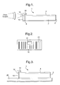
- FIG. 1 there is illustrated diagrammatically a preferred form of apparatus for facilitating the alignment of an optical element, such as a optical fibre, to a further optical element such as an optical integrated waveguide component (IWC) denoted generally by reference numeral 1.
- an optical integrated waveguide component IWC
- the IWC 1 comprises an optically transparent substrate 2 which, in this embodiment, is formed of Gallium Arsenide (GaAs).
- the substrate 2 includes an upper region 4, extending along the length of the substrate, which has a higher refractive index than the remainder of the substrate and forms the waveguide itself.
- a detector is disposed adjacent an output facet 6 of the IWC 1 (i.e. at the end of the IWC distal to the optical fibre) and is arranged to detect a mode signal from the waveguide 4.
- the mode signal is generated when the optical fibre is sufficiently aligned with the waveguide to excite the waveguide mode.
- a mask means in the form of a block 10, is disposed between the optical fibre and the IWC 1 and is arranged to allow light from the optical fibre to pass into, and be transmitted through, the waveguide 4 but to substantially prevent light from being coupled into or transmitted through the substrate 2.
- the mask comprises a block of silicon formed from a conventional silicon wafer.
- the block 10 is sized to have a cross-sectional area A which is equal to or greater than the area of the input facet 8 of the IWC 1 such that it substantially masks the input facet of the IWC.
- the block 10 includes an aperture 12 extending from a front face of the block 10 to a rear face thereof and thus defines an optical transmission pass through the block 10.
- the aperture 12 is disposed in the block 10 such that, when the latter is placed adjacent to the input facet 8 of the IWC 1, the aperture 12 is substantially exactly aligned with the waveguide 4.
- the block 10 is fabricated as follows: a conventional silicon wafer is patterned photolithographically and etched to define a plurality of mask "units", each mask unit having a cross-sectional area equal to or greater than that of the end facet of the IWC 1.
- the aperture 12 is then dry-etched into each of the mask units defined on the silicon wafer, the latter then being diced or cut into the individual mask blocks 10, each block corresponding to a mask unit.
- the aperture 12 is etched such that it passes fully through each individual block 10, thereby to define an optical transmission path through the block.
- the cross-sectional area of the aperture 12 is not constant through the thickness of the block and tapers from the front surface of the block to the rear surface.
- the aperture 12 has a cross-sectional area at the front surface of the block 10 of approximately 25 ⁇ m 2 and a cross-sectional area at the rear surface of the block 10 of 15 ⁇ m 2 .
- the cross-sectional area of the aperture 12 at the rear surface of the block 10 is substantially equal to the cross-sectional area of the waveguide at its front facet.
- the aspect ratio of the cross-sectional area of the aperture at a front surface of the block 10 and the cross-sectional area at a rear surface may be approximately 1.7:1.
- the aspect ratio will vary depending on the thickness of the block 10 and the process used to create the aperture 12.
- Typical waveguide dimensions are between 5 ⁇ m and 10 ⁇ m so an aperture tapered to this at the rear face of the block 10 is desirable.
- the silicon material is also preferably doped to generate free carrier absorption of incident light, thereby substantially preventing light transmission through the block 10 other than by means of the aperture 12.
- the silicon block is thus substantially non-transparent to incident light from the optical fibre, other than through the aperture.
- the block 10 is placed adjacent and in front of the input facet of the IWC 1 such that the aperture 12 is substantially exactly aligned with the waveguide 4. This may be achieved in a number of ways: a first method is to manually abut the block 10 to the input facet 8 of the IWC 1 and adhere the block 10 thereto using an epoxy adhesive or other suitable means.
- a second method is illustrated in Figure 3 and involves mounting the IWC 1 and the block 10 on a silicon motherboard 20 by means of slots etched in the motherboard 20 and corresponding projections on the block 10 and IWC 1.
- the substrate 2 of the IWC 1 is effectively masked such that light from an optical element such as an optical fibre (not shown) is unable to pass therethrough. Only light signals passing through the aperture 12 are transmitted through the IWC 1 and these signals are transmitted substantially entirely by means of the waveguide 4. Consequently, only light transmitted through the waveguide itself will be detected by the detector and, thus, interference to the detector is minimised.
- the optical fibre can be aligned manually with the aperture, the correct position for the optical fibre being determined when the waveguide 4 is excited and the detector detects the optimised mode signal of the waveguide.
- alignment means such as described below, are incorporated in the apparatus.
- Such alignment means enables an appropriate manipulating mechanism, such as a robotic arm or the like for manipulating the optical fibre, to establish the position of the optical fibre relative to the aperture 12 in the block 10.
- a feedback control mechanism such as, for example, a closed-loop algorithmic system, the manipulating mechanism is able to manipulate the optical fibre to align it with the aperture 12 in dependence on the position of the optical fibre.
- the alignment means may advantageously be provided in one of the following ways.
- a series of reflective metal tracks, bars or strips 22 is defined on the front face of the block in the manner of a barcode ( Figure 2).
- Light emitted by the optical fibre is reflected by the bars 22 in the barcode and received by an optical detector associated with the fibre manipulating mechanism.
- a signal processor (not shown) coupled to the optical detector to determine the position of the optical fibre relative to the aperture 12, in dependence on the patterns of light reflected by the barcode.
- the manipulating mechanism is then able to manipulate the optical fibre to adjust its position both vertically and horizontally relative to the block 10 until the optical fibre is substantially exactly aligned with the aperture 12. It will be appreciated that a closed-loop control system is thus defined which enables the manipulating mechanism to determine the position of the optical fibre relative to the block and "home in” on the aperture 12.
- a single reflective line extending across the front face of the block 10 from a point on the periphery of the face to the aperture 12 may be provided. Again, the light from the optical fibre is reflected to the optical detector which causes the manipulating mechanism to "follow" the line, thereby to align the optical fibre with the aperture 12.
- the method by which the manipulating mechanism is able to follow the reflective line is well known in the art of robotics.
- the front face of the block 10 is provided with a two-dimensional array of photodetectors, each of which is arranged to generate a respective positional signal when light from the optical fibre is incident upon them.
- the signals generated by the photodetectors are supplied to a signal processor associated with the manipulating mechanism, which determines therefrom the position of the optical fibre relative to the block.
- a closed-loop feedback control system is provided to enable the manipulating mechanism to "home in” on the aperture 12 in response to the photodetector output signals.
- the silicon micro-aperture block can be used to align optical fibres to both the input and output facets 8, 6 of the IWC 1 and can be used with a variety of waveguide materials, with or without the use of a silicon motherboard or patterned barcode or photodetector array.
- the motherboard and barcode/detector array serve to enhance the methodology and allow a considerable degree of automation to be incorporated in the alignment process.
- the block 10 need not be formed from silicon or, indeed, from a semiconductor material.
- semiconductor materials, and particularly silicon is preferred since the etching process for such materials is well established and it enables photodetector arrays, such as that described above, to be incorporated.
- the block 10 can be formed to have a lip or projection 14 which serves to locate the block correctly relative to the IWC 1 and provides the additional advantage that light from the optical fibre cannot be transmitted to the detector through the air surrounding the IWC.
Landscapes
- Physics & Mathematics (AREA)
- General Physics & Mathematics (AREA)
- Optics & Photonics (AREA)
- Optical Couplings Of Light Guides (AREA)
- Led Device Packages (AREA)
- Light Receiving Elements (AREA)
Abstract
Description
characterised in that the body of the mask means is substantially non-transmissive and non-reflective of light incident thereon from the optical fibre, and wherein the aperture is substantially exactly aligned with the waveguide, thereby to permit light from the optical fibre to be transmitted through the aperture to the waveguide but to substantially prevent light from the optical fibre from passing around at least one of the waveguide and the substrate, or through the substrate.
Claims (20)
- An apparatus for facilitating the alignment of an optical fibre to an integrated waveguide component (1) comprising a substrate (2) having an integral waveguide (4), the apparatus comprising:characterised in that the body of the mask means is substantially non-transmissive and non-reflective of light incident thereon from the optical fibre and wherein, in use, the aperture (12) is substantially exactly aligned with the waveguide (4), thereby to permit light from the optical fibre to be transmitted through the aperture (12) to the waveguide (4) but to substantially prevent light from the optical fibre from passing around at least one of the waveguide (4) and the substrate (2), or through the substrate (2).mask means arranged to be disposed between the optical fibre and the integrated waveguide component (1), the mask means comprising a body including an aperture (12) extending therethrough;
- An apparatus as claimed in claim 1, wherein the mask means has a cross-sectional area greater than or equal to the cross-sectional area of the integrated waveguide component (1).
- An apparatus as claimed in claim 1 or claim 2, wherein the aperture (12) is sized to correspond substantially to the cross-sectional area of the waveguide (4).
- An apparatus as claimed in any of the previous claims, wherein the aperture (12) tapers such that the cross-sectional area thereof reduces from a front surface of the mask means to a rear surface thereof, and wherein the cross-sectional area of the aperture (12) at the rear surface is substantially equal to the cross-sectional area of the waveguide (4).
- An apparatus as claimed in any of the preceding claims, wherein the ratio of the cross-sectional area of the aperture (12) at a front surface of the mask means and the cross-sectional area of the aperture (12) at a rear surface of the mask means is approximately 1.7:1
- An apparatus as claimed in any of the preceding claims, wherein the mask means comprises a block (10) of a semi-conductor material.
- An apparatus as claimed in claim 6, wherein the semiconductor material is silicon.
- An apparatus as claimed in any of the preceding claims, wherein the mask means is formed from a silicon wafer.
- An apparatus as claimed in claim 7 or claim 8, wherein the silicon is doped, thereby to absorb light from the optical fibre.
- An apparatus as claimed in any of the preceding claims further including alignment means for further facilitating alignment of the optical fibre with the aperture (12).
- An apparatus as claimed in claim 10, wherein the alignment means comprises a plurality of reflective strips (22) disposed on the front surface of the mask means substantially in the form of a barcode for reflecting light from the optical fibre.
- An apparatus as claimed in claim 11 further comprising means for detecting light reflected by one or more of the reflective strips (22) and generating a first signal in response thereto.
- An apparatus as claimed in claim 12, further comprising processor means for receiving the first signal, determining the position of the optical fibre relative to the aperture (12) and generating a control signal in dependence thereon.
- An apparatus as claimed in claim 13, further comprising means for manipulating the optical fibre in dependence on the control signal, thereby to align the optical fibre with the aperture (12).
- An apparatus as claimed in claim 10 wherein the alignment means comprises a plurality of detector elements disposed on a front surface of the mask means, each detector element being arranged to detect light from the optical fibre and generate a signal in dependence upon the amount of light detected.
- An apparatus as claimed in claim 15, further comprising processor means for receiving the signal generated by each detector element, determining the position of the optical fibre relative to the aperture (12) from said signals and generating a control signal in response thereto.
- An apparatus as claimed in claim 16, further comprising means for manipulating the optical fibre in dependence on the control signal, thereby to align the optical fibre with the aperture (12).
- A method of aligning an optical fibre to an integrated waveguide component (1) comprising a substrate (2) having an integral waveguide (4), the method comprising:(a) positioning a mask means adjacent an input facet (8) of the integrated waveguide component, the mask means having an aperture (12) extending therethrough,(b) aligning the aperture (12) substantially exactly with the waveguide (4) in the integrated waveguide component (1),(c) manipulating the optical fibre so that light transmitted therefrom is incident upon the mask means,(d) detecting light emitted from an output facet (6) of the integrated waveguide component (1),(e) further manipulating the optical fibre until it attains a desired position, whereby a waveguide mode signal is detected at the output facet (6) of the integrated waveguide component (1), and(f) fixing or securing the optical fibre relative to the integrated waveguide component (1) in said desired position.
- A method of aligning an optical fibre to an integrated waveguide component as claimed in claim 18, comprising the steps of:providing the mask means with a plurality of reflective tracks (22),detecting light reflected by the reflective tracks (22) and generating a first signal in response thereto,determining the position of the optical fibre relative to the aperture (12) and generating a control signal in dependence thereon, andmanipulating the optical fibre in dependence on the control signal, thereby to align the optical fibre with the aperture (12).
- An optical arrangement comprising an integrated waveguide component (1), an optical fibre secured in a fixed position relative to the integrated waveguide component (1), and mask means comprising a body having an aperture (12) extending therethrough, the mask means being disposed between the integrated waveguide component (1) and the optical fibre,
characterised in that the body of the mask means is substantially non-transmissive and non-reflective of light incident thereon from the optical fibre, and wherein the aperture (12) is substantially exactly aligned with the waveguide (4), thereby to permit light from the optical fibre to be transmitted through the aperture (12) to the waveguide (4) but to substantially prevent light from the optical fibre from passing around at least one of the waveguide (4) and the substrate (2), or through the substrate (2).
Applications Claiming Priority (2)
| Application Number | Priority Date | Filing Date | Title |
|---|---|---|---|
| GB0202847 | 2002-02-07 | ||
| GB0202847A GB2385146A (en) | 2002-02-07 | 2002-02-07 | Mask used in alignment of optical fibre and integral waveguide component |
Publications (3)
| Publication Number | Publication Date |
|---|---|
| EP1336880A2 true EP1336880A2 (en) | 2003-08-20 |
| EP1336880A3 EP1336880A3 (en) | 2004-12-29 |
| EP1336880B1 EP1336880B1 (en) | 2008-08-06 |
Family
ID=9930586
Family Applications (1)
| Application Number | Title | Priority Date | Filing Date |
|---|---|---|---|
| EP03250737A Expired - Lifetime EP1336880B1 (en) | 2002-02-07 | 2003-02-05 | Method and apparatus for the alignment of optical components |
Country Status (6)
| Country | Link |
|---|---|
| US (1) | US6882783B2 (en) |
| EP (1) | EP1336880B1 (en) |
| JP (1) | JP2003270481A (en) |
| AT (1) | ATE403886T1 (en) |
| DE (1) | DE60322611D1 (en) |
| GB (1) | GB2385146A (en) |
Cited By (1)
| Publication number | Priority date | Publication date | Assignee | Title |
|---|---|---|---|---|
| WO2006012301A3 (en) * | 2004-06-30 | 2006-05-11 | Teradyne Inc | Connector system for optical wave guides |
Families Citing this family (2)
| Publication number | Priority date | Publication date | Assignee | Title |
|---|---|---|---|---|
| US8786855B2 (en) * | 2011-01-25 | 2014-07-22 | Ocean Optics, Inc. | Shaped input apertures to improve resolution in grating spectrometers |
| CN111638578A (en) * | 2020-06-30 | 2020-09-08 | 中国计量大学 | Automatic light collimation coupling positioning device based on mirror image binocular vision |
Family Cites Families (25)
| Publication number | Priority date | Publication date | Assignee | Title |
|---|---|---|---|---|
| JPS5521057A (en) * | 1978-07-31 | 1980-02-14 | Fujitsu Ltd | Optical transmission line |
| JPS5573011A (en) * | 1978-11-27 | 1980-06-02 | Fujitsu Ltd | Mask forming method of optical fiber and face |
| GB8417911D0 (en) * | 1984-07-13 | 1984-08-15 | British Telecomm | Connecting waveguides |
| GB2184255B (en) * | 1985-12-13 | 1989-01-05 | Stc Plc | Optical fibre integrated optical device coupler |
| GB8827872D0 (en) * | 1988-11-29 | 1988-12-29 | British Telecomm | Optical waveguide method of manufacturing same & system incorporating such waveguide |
| GB9024022D0 (en) * | 1990-11-05 | 1990-12-19 | British Telecomm | Waveguiding structure |
| US5073002A (en) * | 1990-11-30 | 1991-12-17 | Hockaday Bruce D | Self aligning pigtail |
| JPH0540112U (en) * | 1991-05-08 | 1993-05-28 | 三菱マテリアル株式会社 | Positioning device and positioning method for cylindrical container |
| JPH05210027A (en) * | 1991-11-21 | 1993-08-20 | Hitachi Cable Ltd | Waveguide-type optical transmission module coupling part between waveguide and photodetector |
| JPH05341143A (en) * | 1992-06-04 | 1993-12-24 | Hitachi Cable Ltd | Surface mount bidirectional transmission module |
| JPH06204262A (en) * | 1993-01-07 | 1994-07-22 | Fujitsu Ltd | Mounting of optical semiconductor device |
| US5633968A (en) * | 1994-07-18 | 1997-05-27 | Sheem; Sang K. | Face-lock interconnection means for optical fibers and other optical components and manufacturing methods of the same |
| JPH08148668A (en) * | 1994-11-16 | 1996-06-07 | Japan Aviation Electron Ind Ltd | Optical integrated circuit |
| JPH1020135A (en) * | 1996-07-09 | 1998-01-23 | Nikon Corp | Optical waveguide device and method of forming optical thin film |
| KR100236432B1 (en) * | 1996-07-31 | 1999-12-15 | 미야즈 쥰이치로 | Optical polarizer, method for manufacturing same, and blade for manufacturing optical polarizer |
| US5907650A (en) * | 1997-06-26 | 1999-05-25 | Fiberguide Industries, Inc. | High precision optical fiber array connector and method |
| JPH11160568A (en) * | 1997-12-01 | 1999-06-18 | Kyocera Corp | Optical module |
| JPH11353713A (en) * | 1998-06-03 | 1999-12-24 | Sony Music Entertainment (Japan) Inc | Optical recording medium, positioning method therefor, and positioning device |
| JP2000028865A (en) * | 1998-07-09 | 2000-01-28 | Mitsubishi Electric Corp | Semiconductor laser module |
| WO2000028536A1 (en) * | 1998-11-09 | 2000-05-18 | Seiko Instruments Inc. | Near-field optical head and production method thereof |
| GB9919847D0 (en) * | 1999-08-20 | 1999-10-27 | British Telecomm | Alignment device |
| US6438280B1 (en) * | 1999-12-23 | 2002-08-20 | Litton Systems, Inc. | Integrated optics chip having reduced surface wave propagation |
| JP2001305365A (en) * | 2000-04-25 | 2001-10-31 | Nec Corp | Light shielding structure of stray light in optical wavelength module |
| GB2368658A (en) * | 2000-10-31 | 2002-05-08 | Mitel Semiconductor Ab | Aligning optical waveguide with receiver via optical taper |
| GB2385676A (en) * | 2002-02-20 | 2003-08-27 | Bookham Technology Plc | Overhanging waveguide coupled to optic fibre in V groove |
-
2002
- 2002-02-07 GB GB0202847A patent/GB2385146A/en not_active Withdrawn
-
2003
- 2003-02-05 DE DE60322611T patent/DE60322611D1/en not_active Expired - Lifetime
- 2003-02-05 EP EP03250737A patent/EP1336880B1/en not_active Expired - Lifetime
- 2003-02-05 AT AT03250737T patent/ATE403886T1/en not_active IP Right Cessation
- 2003-02-07 US US10/359,563 patent/US6882783B2/en not_active Expired - Fee Related
- 2003-02-07 JP JP2003070973A patent/JP2003270481A/en active Pending
Cited By (3)
| Publication number | Priority date | Publication date | Assignee | Title |
|---|---|---|---|---|
| WO2006012301A3 (en) * | 2004-06-30 | 2006-05-11 | Teradyne Inc | Connector system for optical wave guides |
| US7213974B2 (en) | 2004-06-30 | 2007-05-08 | Amphenol Corporation | Optical waveguide assembly |
| US7561763B2 (en) | 2004-06-30 | 2009-07-14 | Amphenol Corporation | Connector system for optical wave guides |
Also Published As
| Publication number | Publication date |
|---|---|
| EP1336880A3 (en) | 2004-12-29 |
| GB2385146A (en) | 2003-08-13 |
| US6882783B2 (en) | 2005-04-19 |
| JP2003270481A (en) | 2003-09-25 |
| ATE403886T1 (en) | 2008-08-15 |
| US20040017979A1 (en) | 2004-01-29 |
| EP1336880B1 (en) | 2008-08-06 |
| GB0202847D0 (en) | 2002-03-27 |
| DE60322611D1 (en) | 2008-09-18 |
Similar Documents
| Publication | Publication Date | Title |
|---|---|---|
| US5175781A (en) | Attaching optical fibers to integrated optic chips | |
| RU2161323C2 (en) | Device and process of passive matching of optical fiber with input/output light guide ( versions ) | |
| EP1225460A2 (en) | Optical waveguide device and method of manufacturing the same | |
| JPH07202351A (en) | Transmitter and receiver module for two-way optical communication and signal transmission | |
| TWI309313B (en) | Micro-optical device | |
| KR20100014498A (en) | Optical element for free-space propagation between an optical waveguide and another optical waveguide, component, or device | |
| CN102597835A (en) | Substrates and grippers for optical fiber alignment with optical element(s) and related methods | |
| US7209235B2 (en) | Accurate positioning of components of a optical assembly | |
| US6744953B2 (en) | Planar optical waveguide with alignment structure | |
| EP1336880B1 (en) | Method and apparatus for the alignment of optical components | |
| JPH05264870A (en) | Method of manufacturing optical input / output section of optical waveguide and coupling structure of optical input / output section and optical semiconductor element | |
| US5668823A (en) | Injection laser assembly incorporating a monitor photosensor | |
| US6782170B2 (en) | Optical device having a reference mark system | |
| US11971591B2 (en) | Photonic assembly comprising a photonic component optically coupled with a photonic element | |
| JP2630236B2 (en) | Optical transceiver | |
| US6511191B1 (en) | Optical switch system and method for aligning optical axis therein | |
| JP2002344078A (en) | Equipment for monitoring the emission wavelength of lasers | |
| WO1995006853A1 (en) | INTEGRATED 3x3 COUPLER FOR A FIBER OPTIC GYRO | |
| US11022757B1 (en) | Using an anti-reflection coating with a grating coupler | |
| GB2352558A (en) | An optical transmitter | |
| JP3648755B2 (en) | Method for manufacturing waveguide device | |
| JPH04168776A (en) | Optical axis alignment device | |
| JP2005321669A (en) | Optical communication apparatus | |
| JPH0230192A (en) | Semiconductor laser device | |
| JPH10339824A (en) | Platform for optical module and manufacture thereof |
Legal Events
| Date | Code | Title | Description |
|---|---|---|---|
| PUAI | Public reference made under article 153(3) epc to a published international application that has entered the european phase |
Free format text: ORIGINAL CODE: 0009012 |
|
| 17P | Request for examination filed |
Effective date: 20030205 |
|
| AK | Designated contracting states |
Designated state(s): AT BE BG CH CY CZ DE DK EE ES FI FR GB GR HU IE IT LI LU MC NL PT SE SI SK TR |
|
| AX | Request for extension of the european patent |
Extension state: AL LT LV MK RO |
|
| PUAL | Search report despatched |
Free format text: ORIGINAL CODE: 0009013 |
|
| AK | Designated contracting states |
Kind code of ref document: A3 Designated state(s): AT BE BG CH CY CZ DE DK EE ES FI FR GB GR HU IE IT LI LU MC NL PT SE SI SK TR |
|
| AX | Request for extension of the european patent |
Extension state: AL LT LV MK RO |
|
| RIC1 | Information provided on ipc code assigned before grant |
Ipc: 7G 02B 6/42 B Ipc: 7G 02B 6/30 A |
|
| 17Q | First examination report despatched |
Effective date: 20050517 |
|
| AKX | Designation fees paid |
Designated state(s): AT BE BG CH CY CZ DE DK EE ES FI FR GB GR HU IE IT LI LU MC NL PT SE SI SK TR |
|
| 17Q | First examination report despatched |
Effective date: 20050517 |
|
| GRAP | Despatch of communication of intention to grant a patent |
Free format text: ORIGINAL CODE: EPIDOSNIGR1 |
|
| GRAS | Grant fee paid |
Free format text: ORIGINAL CODE: EPIDOSNIGR3 |
|
| GRAA | (expected) grant |
Free format text: ORIGINAL CODE: 0009210 |
|
| AK | Designated contracting states |
Kind code of ref document: B1 Designated state(s): AT BE BG CH CY CZ DE DK EE ES FI FR GB GR HU IE IT LI LU MC NL PT SE SI SK TR |
|
| REG | Reference to a national code |
Ref country code: GB Ref legal event code: FG4D |
|
| REG | Reference to a national code |
Ref country code: CH Ref legal event code: EP |
|
| REG | Reference to a national code |
Ref country code: IE Ref legal event code: FG4D |
|
| REF | Corresponds to: |
Ref document number: 60322611 Country of ref document: DE Date of ref document: 20080918 Kind code of ref document: P |
|
| PG25 | Lapsed in a contracting state [announced via postgrant information from national office to epo] |
Ref country code: ES Free format text: LAPSE BECAUSE OF FAILURE TO SUBMIT A TRANSLATION OF THE DESCRIPTION OR TO PAY THE FEE WITHIN THE PRESCRIBED TIME-LIMIT Effective date: 20081117 Ref country code: NL Free format text: LAPSE BECAUSE OF FAILURE TO SUBMIT A TRANSLATION OF THE DESCRIPTION OR TO PAY THE FEE WITHIN THE PRESCRIBED TIME-LIMIT Effective date: 20080806 |
|
| PG25 | Lapsed in a contracting state [announced via postgrant information from national office to epo] |
Ref country code: FI Free format text: LAPSE BECAUSE OF FAILURE TO SUBMIT A TRANSLATION OF THE DESCRIPTION OR TO PAY THE FEE WITHIN THE PRESCRIBED TIME-LIMIT Effective date: 20080806 Ref country code: AT Free format text: LAPSE BECAUSE OF FAILURE TO SUBMIT A TRANSLATION OF THE DESCRIPTION OR TO PAY THE FEE WITHIN THE PRESCRIBED TIME-LIMIT Effective date: 20080806 Ref country code: SI Free format text: LAPSE BECAUSE OF FAILURE TO SUBMIT A TRANSLATION OF THE DESCRIPTION OR TO PAY THE FEE WITHIN THE PRESCRIBED TIME-LIMIT Effective date: 20080806 |
|
| PG25 | Lapsed in a contracting state [announced via postgrant information from national office to epo] |
Ref country code: BE Free format text: LAPSE BECAUSE OF FAILURE TO SUBMIT A TRANSLATION OF THE DESCRIPTION OR TO PAY THE FEE WITHIN THE PRESCRIBED TIME-LIMIT Effective date: 20080806 |
|
| PG25 | Lapsed in a contracting state [announced via postgrant information from national office to epo] |
Ref country code: BG Free format text: LAPSE BECAUSE OF FAILURE TO SUBMIT A TRANSLATION OF THE DESCRIPTION OR TO PAY THE FEE WITHIN THE PRESCRIBED TIME-LIMIT Effective date: 20081106 Ref country code: DK Free format text: LAPSE BECAUSE OF FAILURE TO SUBMIT A TRANSLATION OF THE DESCRIPTION OR TO PAY THE FEE WITHIN THE PRESCRIBED TIME-LIMIT Effective date: 20080806 |
|
| PG25 | Lapsed in a contracting state [announced via postgrant information from national office to epo] |
Ref country code: PT Free format text: LAPSE BECAUSE OF FAILURE TO SUBMIT A TRANSLATION OF THE DESCRIPTION OR TO PAY THE FEE WITHIN THE PRESCRIBED TIME-LIMIT Effective date: 20090106 Ref country code: CZ Free format text: LAPSE BECAUSE OF FAILURE TO SUBMIT A TRANSLATION OF THE DESCRIPTION OR TO PAY THE FEE WITHIN THE PRESCRIBED TIME-LIMIT Effective date: 20080806 Ref country code: SK Free format text: LAPSE BECAUSE OF FAILURE TO SUBMIT A TRANSLATION OF THE DESCRIPTION OR TO PAY THE FEE WITHIN THE PRESCRIBED TIME-LIMIT Effective date: 20080806 |
|
| PLBE | No opposition filed within time limit |
Free format text: ORIGINAL CODE: 0009261 |
|
| STAA | Information on the status of an ep patent application or granted ep patent |
Free format text: STATUS: NO OPPOSITION FILED WITHIN TIME LIMIT |
|
| 26N | No opposition filed |
Effective date: 20090507 |
|
| PG25 | Lapsed in a contracting state [announced via postgrant information from national office to epo] |
Ref country code: EE Free format text: LAPSE BECAUSE OF FAILURE TO SUBMIT A TRANSLATION OF THE DESCRIPTION OR TO PAY THE FEE WITHIN THE PRESCRIBED TIME-LIMIT Effective date: 20080806 |
|
| PG25 | Lapsed in a contracting state [announced via postgrant information from national office to epo] |
Ref country code: IT Free format text: LAPSE BECAUSE OF FAILURE TO SUBMIT A TRANSLATION OF THE DESCRIPTION OR TO PAY THE FEE WITHIN THE PRESCRIBED TIME-LIMIT Effective date: 20080806 |
|
| PG25 | Lapsed in a contracting state [announced via postgrant information from national office to epo] |
Ref country code: MC Free format text: LAPSE BECAUSE OF NON-PAYMENT OF DUE FEES Effective date: 20090228 |
|
| REG | Reference to a national code |
Ref country code: CH Ref legal event code: PL |
|
| PG25 | Lapsed in a contracting state [announced via postgrant information from national office to epo] |
Ref country code: CH Free format text: LAPSE BECAUSE OF NON-PAYMENT OF DUE FEES Effective date: 20090228 Ref country code: LI Free format text: LAPSE BECAUSE OF NON-PAYMENT OF DUE FEES Effective date: 20090228 |
|
| PG25 | Lapsed in a contracting state [announced via postgrant information from national office to epo] |
Ref country code: IE Free format text: LAPSE BECAUSE OF NON-PAYMENT OF DUE FEES Effective date: 20090205 Ref country code: SE Free format text: LAPSE BECAUSE OF FAILURE TO SUBMIT A TRANSLATION OF THE DESCRIPTION OR TO PAY THE FEE WITHIN THE PRESCRIBED TIME-LIMIT Effective date: 20081106 |
|
| PG25 | Lapsed in a contracting state [announced via postgrant information from national office to epo] |
Ref country code: GR Free format text: LAPSE BECAUSE OF FAILURE TO SUBMIT A TRANSLATION OF THE DESCRIPTION OR TO PAY THE FEE WITHIN THE PRESCRIBED TIME-LIMIT Effective date: 20081107 |
|
| PG25 | Lapsed in a contracting state [announced via postgrant information from national office to epo] |
Ref country code: LU Free format text: LAPSE BECAUSE OF NON-PAYMENT OF DUE FEES Effective date: 20090205 |
|
| PG25 | Lapsed in a contracting state [announced via postgrant information from national office to epo] |
Ref country code: HU Free format text: LAPSE BECAUSE OF FAILURE TO SUBMIT A TRANSLATION OF THE DESCRIPTION OR TO PAY THE FEE WITHIN THE PRESCRIBED TIME-LIMIT Effective date: 20090207 |
|
| PG25 | Lapsed in a contracting state [announced via postgrant information from national office to epo] |
Ref country code: TR Free format text: LAPSE BECAUSE OF FAILURE TO SUBMIT A TRANSLATION OF THE DESCRIPTION OR TO PAY THE FEE WITHIN THE PRESCRIBED TIME-LIMIT Effective date: 20080806 |
|
| PG25 | Lapsed in a contracting state [announced via postgrant information from national office to epo] |
Ref country code: CY Free format text: LAPSE BECAUSE OF FAILURE TO SUBMIT A TRANSLATION OF THE DESCRIPTION OR TO PAY THE FEE WITHIN THE PRESCRIBED TIME-LIMIT Effective date: 20080806 |
|
| PGFP | Annual fee paid to national office [announced via postgrant information from national office to epo] |
Ref country code: FR Payment date: 20120227 Year of fee payment: 10 |
|
| PGFP | Annual fee paid to national office [announced via postgrant information from national office to epo] |
Ref country code: DE Payment date: 20120221 Year of fee payment: 10 |
|
| PGFP | Annual fee paid to national office [announced via postgrant information from national office to epo] |
Ref country code: GB Payment date: 20120221 Year of fee payment: 10 |
|
| GBPC | Gb: european patent ceased through non-payment of renewal fee |
Effective date: 20130205 |
|
| REG | Reference to a national code |
Ref country code: FR Ref legal event code: ST Effective date: 20131031 |
|
| REG | Reference to a national code |
Ref country code: DE Ref legal event code: R119 Ref document number: 60322611 Country of ref document: DE Effective date: 20130903 |
|
| PG25 | Lapsed in a contracting state [announced via postgrant information from national office to epo] |
Ref country code: DE Free format text: LAPSE BECAUSE OF NON-PAYMENT OF DUE FEES Effective date: 20130903 Ref country code: GB Free format text: LAPSE BECAUSE OF NON-PAYMENT OF DUE FEES Effective date: 20130205 Ref country code: FR Free format text: LAPSE BECAUSE OF NON-PAYMENT OF DUE FEES Effective date: 20130228 |