EP1335208A2 - Method and apparatus for the digital and analog triggering - Google Patents
Method and apparatus for the digital and analog triggering Download PDFInfo
- Publication number
- EP1335208A2 EP1335208A2 EP03250827A EP03250827A EP1335208A2 EP 1335208 A2 EP1335208 A2 EP 1335208A2 EP 03250827 A EP03250827 A EP 03250827A EP 03250827 A EP03250827 A EP 03250827A EP 1335208 A2 EP1335208 A2 EP 1335208A2
- Authority
- EP
- European Patent Office
- Prior art keywords
- analog
- digital
- test
- trigger
- input
- Prior art date
- Legal status (The legal status is an assumption and is not a legal conclusion. Google has not performed a legal analysis and makes no representation as to the accuracy of the status listed.)
- Granted
Links
Images

Classifications
-
- G—PHYSICS
- G01—MEASURING; TESTING
- G01R—MEASURING ELECTRIC VARIABLES; MEASURING MAGNETIC VARIABLES
- G01R13/00—Arrangements for displaying electric variables or waveforms
-
- G—PHYSICS
- G01—MEASURING; TESTING
- G01R—MEASURING ELECTRIC VARIABLES; MEASURING MAGNETIC VARIABLES
- G01R1/00—Details of instruments or arrangements of the types included in groups G01R5/00 - G01R13/00 and G01R31/00
- G01R1/02—General constructional details
- G01R1/06—Measuring leads; Measuring probes
- G01R1/067—Measuring probes
- G01R1/06788—Hand-held or hand-manipulated probes, e.g. for oscilloscopes or for portable test instruments
-
- G—PHYSICS
- G01—MEASURING; TESTING
- G01R—MEASURING ELECTRIC VARIABLES; MEASURING MAGNETIC VARIABLES
- G01R13/00—Arrangements for displaying electric variables or waveforms
- G01R13/20—Cathode-ray oscilloscopes
- G01R13/22—Circuits therefor
- G01R13/32—Circuits for displaying non-recurrent functions such as transients; Circuits for triggering; Circuits for synchronisation; Circuits for time-base expansion
-
- G—PHYSICS
- G01—MEASURING; TESTING
- G01R—MEASURING ELECTRIC VARIABLES; MEASURING MAGNETIC VARIABLES
- G01R31/00—Arrangements for testing electric properties; Arrangements for locating electric faults; Arrangements for electrical testing characterised by what is being tested not provided for elsewhere
- G01R31/28—Testing of electronic circuits, e.g. by signal tracer
- G01R31/2851—Testing of integrated circuits [IC]
- G01R31/2886—Features relating to contacting the IC under test, e.g. probe heads; chucks
- G01R31/2891—Features relating to contacting the IC under test, e.g. probe heads; chucks related to sensing or controlling of force, position, temperature
-
- G—PHYSICS
- G01—MEASURING; TESTING
- G01R—MEASURING ELECTRIC VARIABLES; MEASURING MAGNETIC VARIABLES
- G01R31/00—Arrangements for testing electric properties; Arrangements for locating electric faults; Arrangements for electrical testing characterised by what is being tested not provided for elsewhere
- G01R31/28—Testing of electronic circuits, e.g. by signal tracer
- G01R31/3167—Testing of combined analog and digital circuits
-
- G—PHYSICS
- G01—MEASURING; TESTING
- G01R—MEASURING ELECTRIC VARIABLES; MEASURING MAGNETIC VARIABLES
- G01R31/00—Arrangements for testing electric properties; Arrangements for locating electric faults; Arrangements for electrical testing characterised by what is being tested not provided for elsewhere
- G01R31/28—Testing of electronic circuits, e.g. by signal tracer
- G01R31/317—Testing of digital circuits
- G01R31/3181—Functional testing
- G01R31/319—Tester hardware, i.e. output processing circuits
- G01R31/31917—Stimuli generation or application of test patterns to the device under test [DUT]
- G01R31/31926—Routing signals to or from the device under test [DUT], e.g. switch matrix, pin multiplexing
Definitions
- the invention relates generally to the field of signal analysis and, more specifically, to a method and apparatus for the digital and analog triggering of a signal analysis.
- Signal analysis devices such as Logic Analyzers, digital storage oscilloscopes (DSOs) and the like, are utilized to monitor the signal activity in a wide variety of systems.
- Logic Analyzers provide the capability to monitor the logical activity of a digital system.
- the Logic Analyzer is an instrument having, typically, dozens of input channels, a relatively large memory and the ability to disassemble/decode bus states and phases.
- a Logic Analyzer is electrically coupled to a device or system under test via a hardware interface to capture data while the device or system under test steps through a process.
- the Logic Analyzer tests for a preset condition or trigger to control the recording or processing of the signals generated by the device or system under test.
- the conditions or triggers used for Logic Analyzers are typically digital representations of events.
- some Logic Analyzers include "oscilloscopes on a board” that plug into the Logic Analyzer mainframe. These oscilloscopes are separate instruments that are contained in the same enclosure as the Logic Analyzer. In such combination instruments, in order to trigger on analog events (e.g., a runt signal), the user must attach two probes to the same point. The first probe is the digital logic probe for the Logic Analyzer and the second probe is the analog probe for the device under test. Such connection is necessary because the analog-to-digital conversion for the Logic Analyzer is performed in the probe tip. A trigger out signal from the scope unit must then be connected to the Logic Analyzer external trigger input.
- analog events e.g., a runt signal
- the separate analog and digital signal paths provide a means for processing an input test signal and evaluating the test signal for both preset analog conditions and preset digital conditions in to generate respective analog and digital trigger signals in a signal analysis device.
- the subject invention is adapted, in one embodiment, to an apparatus comprising a probe providing a common path for inputting either analog signals and/or digital signals from a circuit under test to the instrument, and a common node at which the input test signals are received and directed in parallel to a digital path and an analog path.
- the digital path is coupled to the node for receiving and processing the input test signals, wherein a digital trigger circuit is coupled to the digital path for evaluating the processed digital signals for preset digital conditions and generating a digital control trigger upon detection of the preset digital conditions.
- the analog path is coupled to the node for receiving and processing the input test signals, wherein an analog trigger circuit is coupled to the analog path for evaluating the processed analog signals for preset analog conditions and generating an analog control trigger upon detection of the preset analog conditions.
- the subject invention will be primarily described within the context of a single-channel, digital signal analysis device such as a Logic Analyzer (LA). However, it will be appreciated by those skilled in the art that the invention may be advantageously employed in any single-channel or multichannel signal measurement or analysis device in which both digital and analog triggering is desirable.
- LA Logic Analyzer
- FIG. 1 depicts a high level block diagram of a Logic Analyzer 100 according to an embodiment of the present invention.
- the Logic Analyzer 100 of FIG. 1 takes advantage of a significant advance in a new Logic Analyzer disclosed in commonly-assigned U.S. Provisional Patent Application number 60/356,453 filed February 11, 2002, which is herein incorporated by reference in its entirety and which discloses an arrangement whereby a signal under test can be conveyed to the input of a Logic Analyzer in analog form.
- the Logic Analyzer 100 of FIG. 1 comprises a single data acquisition probe 102, a common node 101, a data memory 128, a digital trigger circuit 130, an analog trigger circuit 146, and two signal paths; namely a Digital signal path 110 and an Analog signal path 115.
- the Digital signal path 110 is formed using a Comparator 124, a Digital Output Driver 126 and a threshold buffer 122.
- the Analog signal path 115 is formed using an Analog Buffer 140 and an Analog Output Driver 144.
- a test signal from a device under test is typically an analog signal comprising one of two voltage levels (e.g., 0v and 3v, or 0v and 5v) directed to represent either a low logic level or a high logic level, respectively, using a positive logic format.
- This test signal from is received by the probe 102 and communicated to the Digital signal path 110 and the Analog signal path 115 via the common node 101.
- the Digital signal path 110 provides a digital representation of the test signal to the digital trigger circuit 130.
- the digital trigger circuit 130 enables the Logic Analyzer 100 to trigger (control the recording of data signals in a data memory) upon the identification of a preset digital condition(s).
- the Analog signal path 115 provides an analog representation of the test signal to the analog trigger circuit 146.
- the analog trigger circuit 115 enables the Logic Analyzer 100 to trigger (control the recording of data signals in a data memory) upon the identification of a preset analog condition(s).
- the output of the Logic Analyzer 100 is then be communicated to a processing and display device or otherwise processed.
- a test signal from the probe 102 is communicated to the Digital signal path 110 and is coupled to a first input of the Comparator 124.
- the Comparator 124 is a two input amplifier with high gain and a differential output.
- the first input to the Comparator 124 is from the probe 102.
- a second input to the Comparator 124 is coupled to a threshold level voltage from, illustratively, an external pulse generator 120 (and further conditioned by the Threshold Buffer 122).
- the threshold level voltage from the external pulse generator 120 is adjusted by the Threshold Buffer 122 to be substantially equivalent to the voltage at the tip of the probe 102.
- the gain and offset of the Threshold Buffer 122 are adjusted by, illustratively, 7 bits in a control register. The range of values in the control register varies between 0 and 127.
- the values in the control register are selected to represent specific desired results. For example, the value 63 sets the gain of the Threshold Buffer 122 at -1/10. Increasing the value raises the gain by up to 15% and decreasing the value lowers the Gain by up to 15%. The value 63 sets the offset to zero at the output of the Threshold Buffer 122. The value of 0 sets the Buffer output 13mV more negative than normal. The value of 126 sets the Buffer 13mV more positive than normal. The output of the Threshold Buffer 122 then drives the Comparator 124.
- the Comparator 124 compares the test signal voltage (probe voltage) and the threshold level voltage. If the probe voltage is greater than the adjusted threshold voltage, then the output of the Comparator 124 goes to a digital high logic state. The output of the Comparator 124 is coupled to the Digital Output Driver 126.
- the Digital Output Driver 126 comprises, illustratively, a differential non-inverting digital buffer whose output has high drive capability.
- the Digital Output Driver 126 optionally provides a selectable propagation delay.
- the propagation delay is provided by a Delay Select element, comprising a separate element of the Logic Analyzer.
- One bit of a register selects the propagation delay of the Digital Output Driver 126. For example, a value of 0 imparts a minimum (e.g., 0 ps) delay while a value of 1 imparts a maximum (e.g., 62 ps) delay relative to the total propagation delay of the Digital signal path 110.
- the output of the Digital Output Driver 126 is then applied to the data memory 128 and the digital trigger circuit 130 substantially simultaneously.
- the digital trigger circuit 130 evaluates the digital data from the Digital Output Driver 126 for preset conditions (triggers), to control the recording of data signals in the data memory 128.
- Digital trigger circuits and digital trigger conditions such as those of conventional Logic Analyzers, are well known to those skilled in the art and will not be described in detail herein.
- the Analog signal path 115 receives the test signal from the probe 102.
- the test signal is input to a selectable gain Analog Buffer 140.
- the Analog Buffer 140 comprises, illustratively, a differential amplifier with selectable gains.
- the gains of the Analog Buffer 140 can be set to 0 (off/power down), 1, 2, or 3 (maximum gain) by two bits in a control register.
- the output signal of the Analog Buffer 140 is a varying current not a voltage.
- the gain of the Analog Buffer 140 is set in its input stage by two differential amplifier pairs connected in parallel.
- One differential amplifier pair is designed to give a gain of one and the other differential amplifier pair is designed to give a gain of two (set by, for example, an emitter resistor value).
- One amplifier or the other is turned on at a time to give a gain of one or two. Both amplifiers are turned on at once to give a gain of three. The gain of three is achieved because the output currents of the two differential amplifier pair sum together.
- the output signal currents of the Analog Buffer 140 are routed to an analog bus by a switching circuit in the Analog Buffer 140 that allows this signal to drive any one of a possible plurality of buses at a time.
- the limiting capabilities of the Analog Buffer 140 is accomplished by reserving only two bits of a register to control which bus is to be driven and some decoding logic.
- the possibility of a plurality of buses is realized in the case of a Logic Analyzer with multiple input channels. It will be appreciated by one skilled in the art that an Analog Buffer can encompass many embodiments, such as an Analog Buffer with the capability of controlling a plurality of output buses, and still be incorporated within the teachings of the present invention.
- the output signal of the Analog Buffer 140 drives the Analog Output Driver 144
- the Analog Output Driver 144 comprises, illustratively, a non-inverting amplifier that has high drive capability. It has a differential current input and a single ended voltage output.
- the gain and offset of the Analog Output Driver 144 can be adjusted by 7 bits of a control register. The range of values in these registers is 0 to 127.
- the value 63 sets the Gain at nominal. (Nominal is overall analog path gain is about one with the Buffer gain set to 1 and the Analog Output Driver 144 terminated by 50 to 75 ohms.) The gain range is +/-18% around this nominal gain. Increasing the register value raises the Gain. The value 63 sets the Offset to zero relative to the signal (centered).
- the value 0 in the register moves the amplifiers output -16mV and the value 126 moves the amplifier output +16mV if the output is terminated by 50 ohms. (Offset range is +/-19mV if terminated by 75 ohms.)
- the gain and offset adjustments are needed to make up for errors in the overall signal path. Some of these errors are: Probe gain and offset, Probe output impedance, Probe coaxial cable impedance, Receiver input termination mismatch. and Analog Path gain and offset errors.
- the Analog Output Driver 144 can be turned off (powered down) if it is not used. For example, if an OUT_On bit in the Analog Output Driver 144 is set to 0, then the amplifier is off. If the bit is set to 1, the amplifier is on.
- the output of the Analog Output Driver 144 is applied to the analog trigger circuit 146.
- the analog trigger circuit 146 of the Logic Analyzer 100 of FIG. 1 evaluates the analog data from the Analog Output Driver 144 for preset conditions (triggers). Upon detecting such condition(s), a trigger signal from the analog trigger circuit 146 is sent to the digital trigger circuit 130 to cause the digital trigger circuit 130 to begin or continue recording data signals in the data memory 128. Similarly, another trigger signal from the analog trigger circuit 146 can be sent to the digital trigger circuit 130 to end the recording of data in the data memory 128.
- Analog trigger circuits and analog trigger conditions such as the circuits and trigger conditions utilized in conventional oscilloscopes, are well known to those skilled in the art and will not be described in detail herein. For example, some typical analog trigger conditions include runts, glitches, threshold violations, overshoot, ringing, pulse width too high, and pulse width too low conditions.
- analog and digital trigger combinations can be readily devised for controlling the recording of data by a Logic Analyzer that still incorporate these teachings.
- an analog trigger can be employed to begin the recording of data by a Logic Analyzer in accordance with the present invention, while a subsequent digital trigger can be employed to end the recording session and vice-versa.
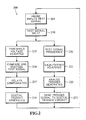
- FIG. 2 depicts a flow diagram of a method according to the present invention.
- the method 200 is entered at step 205, as a test signal from a device under test enters a data acquisition probe such as the probe 102 of FIG. 1.
- the test signal from the data acquisition probe of step 205 is directed at a common node into a digital signal path and an analog signal path.
- the test signal from the probe 102 of FIG. 1 is directed at common node 101 into the Digital signal path 110 and the Analog signal path 115.
- the method 200 then proceeds simultaneously to steps 215 (for the digital signal path) and 220 (for the analog signal path).
- the method 200 will be described referring to digital signal path steps 215-218 and then the analog signal path steps 220-222. It will be appreciated by one skilled in the art that a signal under test can travel substantially simultaneously along the digital signal path and analog signal path.
- a threshold level voltage from an external pulse generator is adjusted by a threshold buffer. That is, at step 215 the threshold level voltage is adjusted by the threshold buffer to be substantially equivalent to the voltage at the tip of the data acquisition probe.
- the adjusted threshold level voltage from the threshold buffer and the test signal from the data acquisition probe are input into a comparator to be evaluated. That is, at step 216, the comparator compares the test signal voltage (probe voltage) and the adjusted threshold level voltage and if the probe voltage is greater than the adjusted threshold voltage, then the output of the comparator produces a first logical state (i.e., a logical high). Conversely, if the probe voltage is less than the adjusted threshold voltage, then the output of the comparator produces a second logical state (i.e., a logical low). As such, the test signal is digitized.
- the output of the Comparator is processed by a Digital Output Driver. That is at step 317, the Digital Output Driver adds a delay to the digitized signal relative to the total propagation delay of the Digital signal path.
- the output of the Digital Output Driver is applied simultaneously to a data memory and to a digital trigger circuit.
- the digital trigger circuit evaluates the digital data from the Digital Output Driver for preset conditions (triggers), to control the recording of data signals in the data memory.
- the method 200 is then exited.
- the test signal from the data acquisition probe is provided to a selectable gain analog buffer in the analog signal path. That is, at step 220, the analog buffer processes the test signal from the probe creating an analog representation of the test signal to be input into an analog output driver.
- the analog buffer selectively couples one of the plurality of analog input signals to an output terminal to be sent to an analog output driver.
- the output of the analog buffer is applied to an analog output driver.
- the gain and offsets of the analog output driver are adjusted to make up for errors in the overall signal path.
- the output of the Analog Output Driver is processed by an analog trigger circuit.
- the analog trigger circuit evaluates the signal from the Analog Output Driver for preset conditions (triggers). The method 200 then proceeds to step 223.
- the analog trigger circuit upon detecting a trigger condition, sends a trigger signal to the digital trigger circuit of step 218 to cause the digital trigger circuit to control the recording of data signals in the data memory.
- the method 200 is then exited.
- a trigger output of the analog trigger circuit can be coupled directly to a data memory to control the recording of data signals in the data memory.
Landscapes
- Physics & Mathematics (AREA)
- General Physics & Mathematics (AREA)
- Engineering & Computer Science (AREA)
- General Engineering & Computer Science (AREA)
- Computer Networks & Wireless Communication (AREA)
- Computer Hardware Design (AREA)
- Microelectronics & Electronic Packaging (AREA)
- Tests Of Electronic Circuits (AREA)
Abstract
Description
Claims (19)
- A test and measurement instrument, comprising:an input conductor for receiving input test signals from a device under test, said input test signals being directed in parallel to a digital path and an analog path;said digital path processing said input test signals to create a digital representation of said input test signals;said analog path processing said input test signals to create an analog representation of said input test signals;a digital trigger circuit coupled to said digital path for evaluating said processed digital signals for preset digital conditions and generating a digital control trigger upon detection of said preset digital conditions; andan analog trigger circuit coupled to said analog path for evaluating said processed analog signals for preset analog conditions and generating an analog control trigger upon detection of said preset analog conditions.
- The test and measurement instrument of claim 1, wherein said analog control trigger from said analog trigger circuit is triggered in response to said analog control trigger.
- The test and measurement instrument of claim 1, further comprising a common node wherein said test signals from said input conductor are directed in parallel to said digital trigger circuit and said analog trigger circuit.
- The test and measurement instrument of claim 1, wherein said input test conductor is a probe.
- The test and measurement instrument of claim 4, wherein said probe is capable of receiving at least one of analog test signals and digital test signals.
- The test and measurement instrument of claim 1, wherein said preset digital conditions are digital trigger words.
- The test and measurement instrument of claim 1, wherein said preset analog conditions are analog trigger words.
- The test and measurement instrument of claim 7, wherein said analog trigger words are selected from the group consisting of runts, glitches, threshold violations, overshoot, ringing, pulse width too high, and pulse width too low conditions.
- The test and measurement instrument of claim 1, wherein said digital path comprises a comparator for determining a logic state of said input test signals and producing a digital representation of said input test signals.
- The test and measurement instrument of claim 1, wherein said analog path comprises an analog buffer for producing an analog representation of said input test signals.
- The test and measurement instrument of claim 1, further comprising a data memory.
- The test and measurement instrument of claim 11, wherein said digital control trigger from said digital trigger circuit is operable for controlling the recording of data in said data memory.
- A method, comprising:processing an input test signal to create a digital representation of said input test signal;processing said input test signal to create an analog representation of said input test signal;generating a digital trigger in response to said digital representation favorably comparing to at least one preset digital condition; andgenerating an analog trigger in response to said analog representation favorably comparing to at least one preset analog condition.
- The method of claim 13, further comprising:receiving said input test signal via a common path.
- The method of claim 14, wherein said test signal is provided to said common path via an input conductor.
- The method of claim 14, wherein said input conductor is a probe.
- The method of claim 13, further comprising:controlling the recording of data in a data memory in response to a favorable comparison of said digital representation.
- The method of claim 13, further comprising:controlling the recording of data in a data memory in response to a favorable comparison of said analog representation.
- The method of claim 13, further comprising:generating a digital control trigger in said digital path in response to an analog control trigger.
Applications Claiming Priority (4)
| Application Number | Priority Date | Filing Date | Title |
|---|---|---|---|
| US35645302P | 2002-02-11 | 2002-02-11 | |
| US356453P | 2002-02-11 | ||
| US316548 | 2002-12-10 | ||
| US10/316,548 US7227349B2 (en) | 2002-02-11 | 2002-12-10 | Method and apparatus for the digital and analog triggering of a signal analysis device |
Publications (3)
| Publication Number | Publication Date |
|---|---|
| EP1335208A2 true EP1335208A2 (en) | 2003-08-13 |
| EP1335208A3 EP1335208A3 (en) | 2003-10-15 |
| EP1335208B1 EP1335208B1 (en) | 2011-01-12 |
Family
ID=27616586
Family Applications (1)
| Application Number | Title | Priority Date | Filing Date |
|---|---|---|---|
| EP03250827A Expired - Lifetime EP1335208B1 (en) | 2002-02-11 | 2003-02-10 | Method and apparatus for the digital and analog triggering |
Country Status (4)
| Country | Link |
|---|---|
| US (1) | US7227349B2 (en) |
| EP (1) | EP1335208B1 (en) |
| JP (1) | JP4582999B2 (en) |
| DE (1) | DE60335683D1 (en) |
Cited By (1)
| Publication number | Priority date | Publication date | Assignee | Title |
|---|---|---|---|---|
| EP1584933A1 (en) * | 2004-04-02 | 2005-10-12 | ATMEL Germany GmbH | Method and device for testing of integrated circuits |
Families Citing this family (6)
| Publication number | Priority date | Publication date | Assignee | Title |
|---|---|---|---|---|
| DE102005035473A1 (en) * | 2005-07-28 | 2007-02-01 | Rohde & Schwarz Gmbh & Co. Kg | Method and system for digital triggering for oscilloscopes |
| GB2455052A (en) * | 2007-09-21 | 2009-06-03 | Agilent Technologies Inc | Trigger event detection apparatus and method therefore |
| US8392626B2 (en) * | 2008-04-24 | 2013-03-05 | Honeywell International Inc. | Programmable channel circuit for coupling signals between field devices and control systems |
| US10825263B2 (en) | 2016-06-16 | 2020-11-03 | Honeywell International Inc. | Advanced discrete control device diagnostic on digital output modules |
| GB2597482B (en) * | 2020-07-22 | 2022-08-24 | Advanced Risc Mach Ltd | A debug probe for measuring at least one property of a target system |
| US20230055303A1 (en) * | 2021-08-23 | 2023-02-23 | Tektronix, Inc. | Parallel trigger paths in a test and measurement instrument |
Family Cites Families (20)
| Publication number | Priority date | Publication date | Assignee | Title |
|---|---|---|---|---|
| US4441183A (en) * | 1982-03-22 | 1984-04-03 | Western Electric Company, Inc. | Apparatus for testing digital and analog circuits |
| US4585975A (en) * | 1983-04-21 | 1986-04-29 | Tektronix, Inc. | High speed Boolean logic trigger oscilloscope vertical amplifier with edge sensitivity and nested trigger |
| US4823076A (en) * | 1986-03-17 | 1989-04-18 | Tektronix, Inc. | Method and apparatus for triggering |
| GB2224869A (en) * | 1988-11-07 | 1990-05-16 | Nicolet Instrument Corp | Digital comparator trigger signal |
| US5214784A (en) * | 1988-11-28 | 1993-05-25 | Tektronix, Inc. | Sequence of events detector for serial digital data which selectively outputs match signal in the series which defines detected sequence |
| JPH0372269A (en) * | 1989-08-11 | 1991-03-27 | Yokogawa Electric Corp | Trigger circuit |
| US5043927A (en) * | 1989-09-18 | 1991-08-27 | Tektronix, Inc. | Digital signal quality analysis using simultaneous dual-threshold data acquisition |
| JPH03162677A (en) | 1989-11-21 | 1991-07-12 | Mitsubishi Electric Corp | Probe for oscilloscope |
| JPH03202783A (en) * | 1989-12-29 | 1991-09-04 | Matsushita Electric Ind Co Ltd | logic analyzer |
| US5235270A (en) * | 1990-03-19 | 1993-08-10 | Yokogawa Electric Corporation | Waveform measuring device |
| JPH04252966A (en) * | 1991-01-29 | 1992-09-08 | Toshiba Corp | Logic analyzer |
| US5123034A (en) * | 1991-05-20 | 1992-06-16 | Tektronix, Inc. | Automatic anomalous event detection |
| JPH04359159A (en) * | 1991-06-06 | 1992-12-11 | Yokogawa Electric Corp | Wave-form observing device |
| JPH05157770A (en) * | 1991-12-09 | 1993-06-25 | Matsushita Electric Ind Co Ltd | Logic analyzer |
| US5274336A (en) * | 1992-01-14 | 1993-12-28 | Hewlett-Packard Company | Capacitively-coupled test probe |
| JPH0815329A (en) | 1994-06-29 | 1996-01-19 | Sony Tektronix Corp | Digital storage oscilloscope |
| JPH1151974A (en) | 1997-07-31 | 1999-02-26 | Nec Home Electron Ltd | Probe adapter |
| JP3758828B2 (en) * | 1997-09-17 | 2006-03-22 | 株式会社キーエンス | Waveform observation device |
| US6421619B1 (en) * | 1998-10-02 | 2002-07-16 | International Business Machines Corporation | Data processing system and method included within an oscilloscope for independently testing an input signal |
| EP1335207B1 (en) * | 2002-02-11 | 2012-10-10 | Tektronix, Inc. | Method and device for capturing a signal |
-
2002
- 2002-12-10 US US10/316,548 patent/US7227349B2/en not_active Expired - Fee Related
-
2003
- 2003-02-06 JP JP2003029330A patent/JP4582999B2/en not_active Expired - Fee Related
- 2003-02-10 DE DE60335683T patent/DE60335683D1/en not_active Expired - Lifetime
- 2003-02-10 EP EP03250827A patent/EP1335208B1/en not_active Expired - Lifetime
Cited By (2)
| Publication number | Priority date | Publication date | Assignee | Title |
|---|---|---|---|---|
| EP1584933A1 (en) * | 2004-04-02 | 2005-10-12 | ATMEL Germany GmbH | Method and device for testing of integrated circuits |
| US7408375B2 (en) | 2004-04-02 | 2008-08-05 | Atmel Germany Gmbh | Method and testing apparatus for testing integrated circuits |
Also Published As
| Publication number | Publication date |
|---|---|
| US20030154452A1 (en) | 2003-08-14 |
| DE60335683D1 (en) | 2011-02-24 |
| JP2003279598A (en) | 2003-10-02 |
| EP1335208A3 (en) | 2003-10-15 |
| US7227349B2 (en) | 2007-06-05 |
| JP4582999B2 (en) | 2010-11-17 |
| EP1335208B1 (en) | 2011-01-12 |
Similar Documents
| Publication | Publication Date | Title |
|---|---|---|
| CA1293863C (en) | Time measurement in automatic test equipment | |
| US6879175B2 (en) | Hybrid AC/DC-coupled channel for automatic test equipment | |
| WO2004023673A1 (en) | Aircraft multi-function wire and insulation tester | |
| JPS6030898B2 (en) | Logic analyzer input device | |
| EP1335208B1 (en) | Method and apparatus for the digital and analog triggering | |
| US20020063553A1 (en) | Method and apparatus for displaying triggered waveform on an error performance analyzer | |
| KR100555544B1 (en) | A device that generates a test stimulus signal with a current source independent of the internal impedance change of the device under test. | |
| US6847199B2 (en) | Capturing both digital and analog forms of a signal through the same probing path | |
| US7285948B2 (en) | Method and apparatus providing single cable bi-directional triggering between instruments | |
| CN112816784B (en) | Resistance test circuit and system | |
| US6191683B1 (en) | System and method for comparing values during logic analysis | |
| US20030020459A1 (en) | Compare path bandwidth control for high performance automatic test systems | |
| US6990416B2 (en) | Qualification signal measurement, trigger, and/or display system | |
| JPH03103770A (en) | Signal analyzing method | |
| EP3531147B1 (en) | Electrical testing apparatus for spintronic devices | |
| EP1380847B1 (en) | Monitor circuitry and method for testing analog and/or mixed signal integrated circuits | |
| US7137061B2 (en) | Method and device for signaling a transmission fault on a data line | |
| US5942982A (en) | System for detecting open circuits with a measurement device | |
| RU2142142C1 (en) | Device locating point of fault in power transmission and communication lines | |
| US5825786A (en) | Undersampling digital testability circuit | |
| CN114518520A (en) | Chip testing system and method | |
| JP3375597B2 (en) | Apparatus and method for testing cross voltage of differential signal | |
| CN222353981U (en) | Device for rapidly measuring high-resistance migration current | |
| US20030200044A1 (en) | Systems and methods for tagging measurement values | |
| US20020011866A1 (en) | Apparatus for testing a semiconductor and process for the same |
Legal Events
| Date | Code | Title | Description |
|---|---|---|---|
| PUAI | Public reference made under article 153(3) epc to a published international application that has entered the european phase |
Free format text: ORIGINAL CODE: 0009012 |
|
| AK | Designated contracting states |
Designated state(s): AT BE BG CH CY CZ DE DK EE ES FI FR GB GR HU IE IT LI LU MC NL PT SE SI SK TR |
|
| AX | Request for extension of the european patent |
Extension state: AL LT LV MK RO |
|
| PUAL | Search report despatched |
Free format text: ORIGINAL CODE: 0009013 |
|
| AK | Designated contracting states |
Kind code of ref document: A3 Designated state(s): AT BE BG CH CY CZ DE DK EE ES FI FR GB GR HU IE IT LI LU MC NL PT SE SI SK TR |
|
| AX | Request for extension of the european patent |
Extension state: AL LT LV MK RO |
|
| RIC1 | Information provided on ipc code assigned before grant |
Ipc: 7G 01R 13/32 B Ipc: 7G 01R 13/00 A |
|
| 17P | Request for examination filed |
Effective date: 20040219 |
|
| AKX | Designation fees paid |
Designated state(s): DE FR GB IT |
|
| 17Q | First examination report despatched |
Effective date: 20080312 |
|
| GRAP | Despatch of communication of intention to grant a patent |
Free format text: ORIGINAL CODE: EPIDOSNIGR1 |
|
| GRAS | Grant fee paid |
Free format text: ORIGINAL CODE: EPIDOSNIGR3 |
|
| GRAA | (expected) grant |
Free format text: ORIGINAL CODE: 0009210 |
|
| AK | Designated contracting states |
Kind code of ref document: B1 Designated state(s): DE FR GB IT |
|
| REG | Reference to a national code |
Ref country code: GB Ref legal event code: FG4D |
|
| REF | Corresponds to: |
Ref document number: 60335683 Country of ref document: DE Date of ref document: 20110224 Kind code of ref document: P |
|
| REG | Reference to a national code |
Ref country code: DE Ref legal event code: R096 Ref document number: 60335683 Country of ref document: DE Effective date: 20110224 |
|
| PLBE | No opposition filed within time limit |
Free format text: ORIGINAL CODE: 0009261 |
|
| STAA | Information on the status of an ep patent application or granted ep patent |
Free format text: STATUS: NO OPPOSITION FILED WITHIN TIME LIMIT |
|
| 26N | No opposition filed |
Effective date: 20111013 |
|
| REG | Reference to a national code |
Ref country code: DE Ref legal event code: R097 Ref document number: 60335683 Country of ref document: DE Effective date: 20111013 |
|
| PGFP | Annual fee paid to national office [announced via postgrant information from national office to epo] |
Ref country code: DE Payment date: 20140227 Year of fee payment: 12 |
|
| PGFP | Annual fee paid to national office [announced via postgrant information from national office to epo] |
Ref country code: FR Payment date: 20140220 Year of fee payment: 12 Ref country code: IT Payment date: 20140225 Year of fee payment: 12 |
|
| PGFP | Annual fee paid to national office [announced via postgrant information from national office to epo] |
Ref country code: GB Payment date: 20140227 Year of fee payment: 12 |
|
| REG | Reference to a national code |
Ref country code: DE Ref legal event code: R119 Ref document number: 60335683 Country of ref document: DE |
|
| GBPC | Gb: european patent ceased through non-payment of renewal fee |
Effective date: 20150210 |
|
| REG | Reference to a national code |
Ref country code: FR Ref legal event code: ST Effective date: 20151030 |
|
| PG25 | Lapsed in a contracting state [announced via postgrant information from national office to epo] |
Ref country code: IT Free format text: LAPSE BECAUSE OF NON-PAYMENT OF DUE FEES Effective date: 20150210 |
|
| PG25 | Lapsed in a contracting state [announced via postgrant information from national office to epo] |
Ref country code: DE Free format text: LAPSE BECAUSE OF NON-PAYMENT OF DUE FEES Effective date: 20150901 Ref country code: GB Free format text: LAPSE BECAUSE OF NON-PAYMENT OF DUE FEES Effective date: 20150210 |
|
| PG25 | Lapsed in a contracting state [announced via postgrant information from national office to epo] |
Ref country code: FR Free format text: LAPSE BECAUSE OF NON-PAYMENT OF DUE FEES Effective date: 20150302 |