EP1333493A2 - Interconnect structure - Google Patents
Interconnect structure Download PDFInfo
- Publication number
- EP1333493A2 EP1333493A2 EP03250202A EP03250202A EP1333493A2 EP 1333493 A2 EP1333493 A2 EP 1333493A2 EP 03250202 A EP03250202 A EP 03250202A EP 03250202 A EP03250202 A EP 03250202A EP 1333493 A2 EP1333493 A2 EP 1333493A2
- Authority
- EP
- European Patent Office
- Prior art keywords
- interconnect
- devices
- test
- substrate
- interconnect structure
- Prior art date
- Legal status (The legal status is an assumption and is not a legal conclusion. Google has not performed a legal analysis and makes no representation as to the accuracy of the status listed.)
- Withdrawn
Links
Images




Classifications
-
- G—PHYSICS
- G01—MEASURING; TESTING
- G01R—MEASURING ELECTRIC VARIABLES; MEASURING MAGNETIC VARIABLES
- G01R1/00—Details of instruments or arrangements of the types included in groups G01R5/00 - G01R13/00 and G01R31/00
- G01R1/02—General constructional details
- G01R1/04—Housings; Supporting members; Arrangements of terminals
- G01R1/0408—Test fixtures or contact fields; Connectors or connecting adaptors; Test clips; Test sockets
-
- H—ELECTRICITY
- H10—SEMICONDUCTOR DEVICES; ELECTRIC SOLID-STATE DEVICES NOT OTHERWISE PROVIDED FOR
- H10W—GENERIC PACKAGES, INTERCONNECTIONS, CONNECTORS OR OTHER CONSTRUCTIONAL DETAILS OF DEVICES COVERED BY CLASS H10
- H10W72/00—Interconnections or connectors in packages
-
- H—ELECTRICITY
- H10—SEMICONDUCTOR DEVICES; ELECTRIC SOLID-STATE DEVICES NOT OTHERWISE PROVIDED FOR
- H10W—GENERIC PACKAGES, INTERCONNECTIONS, CONNECTORS OR OTHER CONSTRUCTIONAL DETAILS OF DEVICES COVERED BY CLASS H10
- H10W72/00—Interconnections or connectors in packages
- H10W72/60—Strap connectors, e.g. thick copper clips for grounding of power devices
-
- G—PHYSICS
- G01—MEASURING; TESTING
- G01R—MEASURING ELECTRIC VARIABLES; MEASURING MAGNETIC VARIABLES
- G01R1/00—Details of instruments or arrangements of the types included in groups G01R5/00 - G01R13/00 and G01R31/00
- G01R1/02—General constructional details
- G01R1/06—Measuring leads; Measuring probes
- G01R1/067—Measuring probes
- G01R1/073—Multiple probes
-
- G—PHYSICS
- G01—MEASURING; TESTING
- G01R—MEASURING ELECTRIC VARIABLES; MEASURING MAGNETIC VARIABLES
- G01R31/00—Arrangements for testing electric properties; Arrangements for locating electric faults; Arrangements for electrical testing characterised by what is being tested not provided for elsewhere
- G01R31/28—Testing of electronic circuits, e.g. by signal tracer
- G01R31/282—Testing of electronic circuits specially adapted for particular applications not provided for elsewhere
- G01R31/2831—Testing of materials or semi-finished products, e.g. semiconductor wafers or substrates
-
- G—PHYSICS
- G01—MEASURING; TESTING
- G01R—MEASURING ELECTRIC VARIABLES; MEASURING MAGNETIC VARIABLES
- G01R31/00—Arrangements for testing electric properties; Arrangements for locating electric faults; Arrangements for electrical testing characterised by what is being tested not provided for elsewhere
- G01R31/28—Testing of electronic circuits, e.g. by signal tracer
- G01R31/2851—Testing of integrated circuits [IC]
Definitions
- the present inventions are related to interconnect structures and, more specifically, to interconnect structures that may, for example, be used in conjunction with testing equipment.
- Interconnect structures are used in a wide variety of applications to electrically connect two devices to one another. Although the present inventions are not limited to any particular application, one application of interconnect structures is associated with the test procedures that are performed on wafers that include semiconductor components both during and after the fabrication process. The tests require that temporary electrical contact be made with contacts on the semiconductor components so that signals may be transferred to and from the components during the tests. Conventional testing equipment typically includes a series of pin contacts for this purpose. The pin contacts are part of an interconnect structure (sometimes referred to as a "probe card") that is manufactured using mechanical machining and assembly processes. Some wafers also have components, such as electron emitters, which emit signals that can be sensed to determine whether the component is operating properly. Some wafers are also tested with probes that supply a predetermined stimulus, such as light, to a particular component. The response to the stimulus, e.g. an electrical or optical signal, is then measured to determine whether the component is functioning properly.
- a predetermined stimulus such as light
- the density and number of semiconductor component contacts has, of course, increased as semiconductor components have become smaller and smaller.
- the inventor herein has determined that, given the ever increasing density of semiconductor component contacts, conventional interconnect structures and the methods of manufacturing such interconnect structures are susceptible to improvement. For example, it is difficult, labor intensive and expensive to manufacture conventional pin contacts because the locational tolerances, both in and out of the semiconductor component plane, have become smaller as the density of the semiconductor component contacts has increased.
- the increased number of component contacts has resulted in a corresponding increase in the number of pin contacts, which further increases the cost of manufacture.
- the inventor herein has also determined that the conventional methods of sensing emissions from wafer components, which is to do the testing after wafer has been diced and additional manufacturing steps (such as packaging) are performed on the individual chips, can be inefficient because the additional manufacturing steps are wasted in those instances where the wafer component is ultimately shown to be defective.
- An interconnect structure in accordance with one embodiment of a present invention includes a substrate, an interconnect device formed on the substrate, and a test device formed on the substrate.
- Such an interconnect structure provides a number of advantages over conventional interconnect structures.
- the present interconnect structures may be manufactured with processes, such as photolithographic processes, that facilitate greater density and locational tolerances and reduce marginal costs.
- the present inventions also enable the emissions from wafer components to be tested earlier in the manufacturing process, such as prior to dicing, which eliminates the inefficiencies associated with performing additional manufacturing steps (such as packaging) on a defective chip.
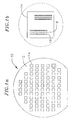
- the semiconductor substrate 10 (or "test substrate” consists of a semiconductor wafer 12 and a plurality of identical dice 14 formed thereon. Each die 14 is provided with a plurality of component contacts 16, such as pads, arranged in a predetermined pattern. In the illustrated example, the pattern consists of four columns of contacts 16. Each die 14 also includes a plurality of testable devices 18, including devices whose emissions are susceptible to being sensed (referred herein as “sensed devices”) and/or devices that are susceptible to being probed (referred to herein as “probed devices").
- sensed devices devices whose emissions are susceptible to being sensed
- probed devices devices that are susceptible to being probed
- Sensed devices include, for example, devices that emit electron beams, such as those used in atomic resolution storage (“ARS”) and field emission device (“FED”) displays, devices that emit light, such as light emitting diodes (“LEDs”), and devices that create a magnetic field.
- Probed devices include, for example, digital micro-mirrors and other optical switches, micro electro-mechanical systems (“MEMS”) motors and movable beams.
- the testable devices 18 are arranged in a predetermined pattern that consists of two columns, each between a respective pair of columns of contacts 16. It should be noted that specifics details concerning the substrate 10 are only provided to the extent that they are useful in illustrating how embodiments of the present inventions may be configured for specific applications and the substrate 10 is merely one example of such an application.
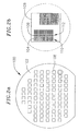
- an interconnect structure 100 in accordance with one embodiment of a present invention includes a base structure 102, which is preferably in the form of a silicon wafer, a glass wafer, a quartz wafer, a gallium arsenide wafer, or a wafer formed from other semiconducting or insulating materials, or any other desired material, that carries a plurality of interconnect devices 104 and test devices 106.
- the interconnect devices 104 and test devices 106 are arranged in sub-arrays 108 that correspond to respective dice.
- Each sub-array 108 in the exemplary embodiment includes four columns 110 of the interconnect devices 104 positioned in a manner corresponding to the position of the contacts 16 on the dice 14.
- the sub-arrays 108 also include two columns 112 of the test devices 106. So configured, each of the contacts 16 may be engaged by a corresponding interconnect device 104, and each of the testable devices 18 may be aligned with a corresponding test device 106, during testing procedure.
- the configuration of the interconnect structure 100 in general, and the type, number, size, spacing and configuration of the interconnect devices 104 and test devices 106 in particular, will vary. Factors which influence the configuration of the interconnect structure 100, interconnect devices 104 and test devices 106 include the configuration of the device being tested (e.g. the semiconductor substrate 10) and the testing protocol.
- the interconnect devices are preferably resilient and movable in the Z-direction to facilitate reliable contact during testing procedures.
- the exemplary interconnect devices 104 include a deflectable beam structure 114 that carries a contact pad 116.
- the deflectable beam structure 114 consists of a main beam portion 118, an intermediate beam portion 120, and a base beam portion 122 that is mounted on the base structure 102.
- a space 124 is defined between the main beam portion 118 and the base structure 102 to enable deflection of the beam structure 114.
- Such deflection is advantageous because it increases the force between the contact pad 116 and the corresponding contact 16 on the test substrate.
- the amount of force is a function of the geometry of the beam structure 114 (i.e. length, width and thickness), the properties of the materials used to form the beam structure (primarily the elasticity and stress of the material), and the amount of beam deflection.
- each of the exemplary interconnect devices 104 also includes an electrical conductor 126 that extends from the contact pad 116 to an electrical conductor 128, which itself extends from the top surface 130 of the base structure 102 (as oriented in Figure 4) to the bottom surface 132.
- the bottom surface side of the electrical conductors 128 may be connected to semiconductor component test equipment.
- the electrical conductors 128 may be positioned relative to one another differently than the associated interconnect devices 104 and, in particular, may be spaced apart from one another by greater distances than the interconnect devices.
- This arrangement facilitates the connection of the bottom surface side of the electrical conductors 128 to be connected to, for example, test equipment using conventional electro-mechanical connectors such as pogo pins.
- an arrangement of high density arrangement of contact pads 116 with a small pitch may be connected to test equipment connectors that have a larger pitch.
- the test devices 106 in the exemplary interconnect structure 100 are electron collectors that measure properties of electron beams such as total current.
- the exemplary test devices 106 include a raised platform 134 and a collector 136 that is formed from conductive material.
- a conductor 138 connects the collector 136 to circuitry, such as multiplexing and amplifier circuits (discussed below), that is also formed on the substrate 102.
- the multiplexing circuits simplify and reduce the number of connections between the interconnect structure 100 and the test equipment (or "system"), while the on-board amplifier circuits provide a better signal-to-noise ratio than would be obtained if the amplifier circuits were not formed on the substrate 102.
- test devices 106 may be used to measure electron dispersion (by measuring current as a function of collector surface bias), electron beam spot size (by breaking the collector surface into segments that are smaller than the spot) and current distribution and diameter (a function of the current to each segment together with their respective sizes and locations). It should also be noted that other types of test devices, including the test devices disclosed herein, may used in conjunction with electron detectors in interconnect structures as applications so require.
- test device Another type of test device that may be incorporated into embodiments of the present inventions, alone or in combination with other types of test devices, is a light detector.
- Technologies such as silicon-based photovoltaic and photodiode technologies may, for example, be used to measure the quantity of visible and near visible light (both infrared and ultraviolet) that is emitted from an optical source, such as an LED, on a substrate.
- the specific type of test device will, of course, depend on the optical source being sensed. Because the interconnect structure 100 may be placed in close proximity with accurate (e.g. better than 1 micron) alignment, an array of light detectors may be used to take spatially defined measurements. Dielectric optical coatings which form bandpass filters may also be used to measure the spectral distributions of optical sources.
- test device Another type of test device that may be incorporated into embodiments of the present inventions, alone or in combination with other types of test devices, is a magnetic field detector, such as a hall effect sensor
- Still another type of device that may be incorporated into interconnect structures in accordance with the present inventions is a probe that supplies a predetermined stimulus, such as light, to a particular component.
- a predetermined stimulus such as light
- the response to the stimulus e.g. an electrical or optical signal
- Such probes may include, for example, LEDs and laser diodes that are formed on the base structure 102.
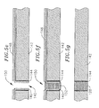
- FIG. 5a-5n An exemplary process for manufacturing interconnect structures in accordance with the present inventions is illustrated in Figures 5a-5n.
- the process preferably takes advantage of MEMS and photolithography manufacturing techniques including wet and dry deposit and etch processes and lift off processes to form interconnect structures on a wafer.
- the explanation of the various process steps refer to a single interconnect device and test device, it should be understood that the present processes may be used to simultaneously form a plurality of interconnect and test devices in a predetermined pattern, such as the pattern illustrated in Figures 2a and 2b.
- the processes may be used to form an interconnect structures that includes a variety of different interconnect devices and/or test devices.
- the exemplary process may be used to manufacture the interconnect structure 100, including the interconnect devices 104 and test devices 106, illustrated in Figures 2a-4.
- the first portion of the exemplary process forms the electrical conductors 128 and begins with the formation of a hole 140 in a wafer 142, such as a thermal oxide silicon wafer.
- a suitable hole formation method is a deep reactive ion etch process such as the Bosch process.
- the surface of the hole 140 is then passivated by, for example, growing an oxide layer 144 on the surface (as shown) or depositing a dielectric layer on the surface.
- a conductive seed layer 146 such as chromium layer with a copper layer over the chromium layer, is then deposited onto the top surface (as oriented in Figures 5a-5n) of the wafer 142 and surface of the oxide layer 144.
- a photoresist pattern 148 is then formed on the conductive seed layer 146 that has a hole 150 that is slightly larger than the portion of the hole 140 that remains after the oxide layer 144 and conductive seed layer are formed.
- Electroplating material 152 such as copper, gold or palladium, is used to fill the hole 140.
- the electroplating material 152 will merge with the conductive seed layer 146 to form the conductor 128.
- circuitry such as analog and CMOS multiplexer and amplifier circuits and circuits with higher level functions such as analog-to-digital converters and signal comparators, that will be associated with the test devices 106.
- circuitry may be formed by photolithography or other suitable methods.
- the circuitry may be connected to electrical conductors 128 that extend to the bottom side of the wafer 142 for connection to, for example, a test system.
- Passivation layers 154a and 154b are then deposited on both sides of the wafer 142 (and over the aforementioned test device circuitry) to protect the wafer and circuitry.
- the regions of the passivation layers 154a and 154b over the conductors 128 and the contact points between the test device circuitry and the test device 106 are etched away. [Figure 5h.]
- the platform 134 for the test device 106 is then formed by depositing and etching a layer of tetraethylorthosilane ("TEOS").
- a sacrificial layer 156 such as a layer of borophosphosilicate glass ("BPSG") or other suitable material, is deposited onto the passivation layer 154a and etched in the manner shown.
- BPSG borophosphosilicate glass
- a layer of beam material is then deposited and etched to form the beam structure 114.
- Suitable beam materials include polysilicon and other suitable metals.
- the formation of the conductor 126, collector 136 and conductor 138 is the next portion of the exemplary process. This may be accomplished by depositing a layer of conductive material, such as aluminum, titanium, palladium and titanium nitride, over at least the beam structure 114, conductor 128, platform 134 and passivation layer 154a, and sacrificial layer 146. The conductive layer is then etched as appropriate to form the conductor 126, collector 136 and conductor 138. [Figure 5l.] This step also completes the formation of the exemplary test devices 106 which, as noted above, are electron collectors.
- a layer of conductive material such as aluminum, titanium, palladium and titanium nitride
- the contact pad 116 is then formed near the free end of the beam structure 114 by depositing and etching a layer of conductive material such as gold, aluminum, titanium, tin, molybdenum, tungsten, or titanium nitride, depending on the intended application.
- a layer of conductive material such as gold, aluminum, titanium, tin, molybdenum, tungsten, or titanium nitride, depending on the intended application.
- Gold is preferred because of its resistance to oxidation.
- the remaining portion of the sacrificial layer 156 is then etched away to form the space 124 between the main beam portion 118 and the base structure 102, which enables deflection of the beam structure 114.
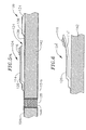
- interconnect device 104' in accordance with another preferred embodiment is illustrated in Figure 6.
- the interconnect device 104' is substantially similar to interconnect device 104. Similar reference numerals are used to represent similar structural elements and the exemplary method described above may be used for the most part to form the interconnect device.
- the beam structure 114' is pre-stressed in the manner shown in order to increase the amount of contact force between the contact pad 116 and the test substrate.
- the beam structure 114' may be manufactured by, for example, forming multiple layers of beam material (instead of one) using a thin film deposition process that leaves the beam structure under compressive stress when completed.
- an exemplary test system 200 in accordance with a preferred embodiment of a present invention includes a wafer handling system with a chuck 202 that aligns the semiconductor substrate 10 with the interconnect structure 100, a test head 204 that supports the interconnect structure, and a control system 206 including test circuitry 208, a processor 210 and an operator interface 212.
- the wafer handling system moves the chuck 202 in the X, Y and/or Z directions to bring the interconnect devices 104 into contact with the component contacts 16 on the semiconductor substrate 10 and to align the test devices 106 with the testable devices 18.
- Test devices 106 interface through circuitry 129 to conductors 128.
- the test circuitry 208 sends and receives signals associated with the testing processes by way of the interconnect structure 100.
- an interface board 214 connects the conductors 128 to the control system 206.
Landscapes
- Physics & Mathematics (AREA)
- General Physics & Mathematics (AREA)
- Testing Or Measuring Of Semiconductors Or The Like (AREA)
- Tests Of Electronic Circuits (AREA)
- Printing Elements For Providing Electric Connections Between Printed Circuits (AREA)
- Wire Bonding (AREA)
- Detection And Correction Of Errors (AREA)
Abstract
Description
- The present inventions are related to interconnect structures and, more specifically, to interconnect structures that may, for example, be used in conjunction with testing equipment.
- Interconnect structures are used in a wide variety of applications to electrically connect two devices to one another. Although the present inventions are not limited to any particular application, one application of interconnect structures is associated with the test procedures that are performed on wafers that include semiconductor components both during and after the fabrication process. The tests require that temporary electrical contact be made with contacts on the semiconductor components so that signals may be transferred to and from the components during the tests. Conventional testing equipment typically includes a series of pin contacts for this purpose. The pin contacts are part of an interconnect structure (sometimes referred to as a "probe card") that is manufactured using mechanical machining and assembly processes. Some wafers also have components, such as electron emitters, which emit signals that can be sensed to determine whether the component is operating properly. Some wafers are also tested with probes that supply a predetermined stimulus, such as light, to a particular component. The response to the stimulus, e.g. an electrical or optical signal, is then measured to determine whether the component is functioning properly.
- The density and number of semiconductor component contacts has, of course, increased as semiconductor components have become smaller and smaller. The inventor herein has determined that, given the ever increasing density of semiconductor component contacts, conventional interconnect structures and the methods of manufacturing such interconnect structures are susceptible to improvement. For example, it is difficult, labor intensive and expensive to manufacture conventional pin contacts because the locational tolerances, both in and out of the semiconductor component plane, have become smaller as the density of the semiconductor component contacts has increased. Moreover, the increased number of component contacts has resulted in a corresponding increase in the number of pin contacts, which further increases the cost of manufacture. The inventor herein has also determined that the conventional methods of sensing emissions from wafer components, which is to do the testing after wafer has been diced and additional manufacturing steps (such as packaging) are performed on the individual chips, can be inefficient because the additional manufacturing steps are wasted in those instances where the wafer component is ultimately shown to be defective.
- Detailed description of preferred embodiments of the inventions will be made with reference to the accompanying drawings.
- Figure 1a is a plan view of an exemplary semiconductor substrate.
- Figure 1b is a partial plan view of the semiconductor substrate illustrated in Figure 1a.
- Figure 2a is a plan view of an interconnect structure including an array of interconnect devices and test devices in accordance with a preferred embodiment of a present invention.
- Figure 2b is a plan view of a sub-array of interconnect devices and test devices in the interconnect structure illustrated in Figure 2a.
- Figure 3 is a partial plan view of a portion of the sub-array of interconnect devices and test devices illustrated in Figure 2b.
- Figure 4 is a side view of an interconnect device and a test device in accordance with a preferred embodiment of a present invention.
- Figures 5a-5n are side, partial section views showing various steps of an interconnect structure manufacturing process in accordance with a preferred embodiment of a present invention.
- Figure 6 is a side view of a portion of an interconnect structure in accordance with a preferred embodiment of a present invention.
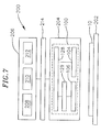
- Figure 7 is a diagrammatic view of a test system in accordance with a preferred embodiment of a present invention.
-
- An interconnect structure in accordance with one embodiment of a present invention includes a substrate, an interconnect device formed on the substrate, and a test device formed on the substrate. Such an interconnect structure provides a number of advantages over conventional interconnect structures. For example, the present interconnect structures may be manufactured with processes, such as photolithographic processes, that facilitate greater density and locational tolerances and reduce marginal costs. The present inventions also enable the emissions from wafer components to be tested earlier in the manufacturing process, such as prior to dicing, which eliminates the inefficiencies associated with performing additional manufacturing steps (such as packaging) on a defective chip.
- The following is a detailed description of the best presently known modes of carrying out the inventions. This description is not to be taken in a limiting sense, but is made merely for the purpose of illustrating the general principles of the inventions. Additionally, it is noted that detailed discussions of various internal operating components, such as specific details of the semiconductor component test equipment, have been omitted for the sake of simplicity. Also, although the exemplary embodiments are described in the context of semiconductor component test equipment, the present inventions are not limited to interconnect structures that are used with any particular apparatus.
- One specific example of a semiconductor substrate that may be tested using equipment containing the present interconnect devices is a
semiconductor substrate 10 illustrated in Figures 1a and 1b. The semiconductor substrate 10 (or "test substrate" consists of asemiconductor wafer 12 and a plurality ofidentical dice 14 formed thereon. Each die 14 is provided with a plurality ofcomponent contacts 16, such as pads, arranged in a predetermined pattern. In the illustrated example, the pattern consists of four columns ofcontacts 16. Each die 14 also includes a plurality oftestable devices 18, including devices whose emissions are susceptible to being sensed (referred herein as "sensed devices") and/or devices that are susceptible to being probed (referred to herein as "probed devices"). Sensed devices include, for example, devices that emit electron beams, such as those used in atomic resolution storage ("ARS") and field emission device ("FED") displays, devices that emit light, such as light emitting diodes ("LEDs"), and devices that create a magnetic field. Probed devices include, for example, digital micro-mirrors and other optical switches, micro electro-mechanical systems ("MEMS") motors and movable beams. In the illustrated example, thetestable devices 18 are arranged in a predetermined pattern that consists of two columns, each between a respective pair of columns ofcontacts 16. It should be noted that specifics details concerning thesubstrate 10 are only provided to the extent that they are useful in illustrating how embodiments of the present inventions may be configured for specific applications and thesubstrate 10 is merely one example of such an application. - As illustrated for example in Figures 2a and 2b, an
interconnect structure 100 in accordance with one embodiment of a present invention includes abase structure 102, which is preferably in the form of a silicon wafer, a glass wafer, a quartz wafer, a gallium arsenide wafer, or a wafer formed from other semiconducting or insulating materials, or any other desired material, that carries a plurality ofinterconnect devices 104 andtest devices 106. In the exemplary embodiment, which is configured to test semiconductor components arranged in a plurality ofdice 14 as illustrated in Figures 1a and 1b, theinterconnect devices 104 andtest devices 106 are arranged insub-arrays 108 that correspond to respective dice. Eachsub-array 108 in the exemplary embodiment includes fourcolumns 110 of theinterconnect devices 104 positioned in a manner corresponding to the position of thecontacts 16 on thedice 14. Thesub-arrays 108 also include twocolumns 112 of thetest devices 106. So configured, each of thecontacts 16 may be engaged by acorresponding interconnect device 104, and each of thetestable devices 18 may be aligned with acorresponding test device 106, during testing procedure. - Of course, in other implementations and as other applications require, the configuration of the
interconnect structure 100 in general, and the type, number, size, spacing and configuration of theinterconnect devices 104 andtest devices 106 in particular, will vary. Factors which influence the configuration of theinterconnect structure 100,interconnect devices 104 andtest devices 106 include the configuration of the device being tested (e.g. the semiconductor substrate 10) and the testing protocol. - Although not so limited, the interconnect devices are preferably resilient and movable in the Z-direction to facilitate reliable contact during testing procedures. Turning to Figures 3 and 4, the
exemplary interconnect devices 104 include adeflectable beam structure 114 that carries acontact pad 116. Thedeflectable beam structure 114 consists of amain beam portion 118, anintermediate beam portion 120, and abase beam portion 122 that is mounted on thebase structure 102. Aspace 124 is defined between themain beam portion 118 and thebase structure 102 to enable deflection of thebeam structure 114. Such deflection is advantageous because it increases the force between thecontact pad 116 and thecorresponding contact 16 on the test substrate. The amount of force is a function of the geometry of the beam structure 114 (i.e. length, width and thickness), the properties of the materials used to form the beam structure (primarily the elasticity and stress of the material), and the amount of beam deflection. - A device that conducts signals from the
contact pads 116 to the portion of theinterconnect structure 100 to which the test equipment is connected must also be provided. One method of providing such a conductor is to simply form thebeam structure 114 from conductive material. Dielectric beam materials are, however, used in the preferred embodiment because of their mechanical properties. Accordingly, each of theexemplary interconnect devices 104 also includes anelectrical conductor 126 that extends from thecontact pad 116 to anelectrical conductor 128, which itself extends from thetop surface 130 of the base structure 102 (as oriented in Figure 4) to thebottom surface 132. The bottom surface side of theelectrical conductors 128 may be connected to semiconductor component test equipment. - Referring more specifically to Figure 3, the
electrical conductors 128 may be positioned relative to one another differently than the associatedinterconnect devices 104 and, in particular, may be spaced apart from one another by greater distances than the interconnect devices. This arrangement facilitates the connection of the bottom surface side of theelectrical conductors 128 to be connected to, for example, test equipment using conventional electro-mechanical connectors such as pogo pins. As such, an arrangement of high density arrangement ofcontact pads 116 with a small pitch may be connected to test equipment connectors that have a larger pitch. - Although not limited to any particular type of test device, the
test devices 106 in theexemplary interconnect structure 100 are electron collectors that measure properties of electron beams such as total current. As illustrated for example in Figures 3 and 4, theexemplary test devices 106 include a raisedplatform 134 and acollector 136 that is formed from conductive material. Aconductor 138 connects thecollector 136 to circuitry, such as multiplexing and amplifier circuits (discussed below), that is also formed on thesubstrate 102. The multiplexing circuits simplify and reduce the number of connections between theinterconnect structure 100 and the test equipment (or "system"), while the on-board amplifier circuits provide a better signal-to-noise ratio than would be obtained if the amplifier circuits were not formed on thesubstrate 102. In addition to total current, thetest devices 106 may be used to measure electron dispersion (by measuring current as a function of collector surface bias), electron beam spot size (by breaking the collector surface into segments that are smaller than the spot) and current distribution and diameter (a function of the current to each segment together with their respective sizes and locations). It should also be noted that other types of test devices, including the test devices disclosed herein, may used in conjunction with electron detectors in interconnect structures as applications so require. - Another type of test device that may be incorporated into embodiments of the present inventions, alone or in combination with other types of test devices, is a light detector. Technologies such as silicon-based photovoltaic and photodiode technologies may, for example, be used to measure the quantity of visible and near visible light (both infrared and ultraviolet) that is emitted from an optical source, such as an LED, on a substrate. The specific type of test device will, of course, depend on the optical source being sensed. Because the
interconnect structure 100 may be placed in close proximity with accurate (e.g. better than 1 micron) alignment, an array of light detectors may be used to take spatially defined measurements. Dielectric optical coatings which form bandpass filters may also be used to measure the spectral distributions of optical sources. - Another type of test device that may be incorporated into embodiments of the present inventions, alone or in combination with other types of test devices, is a magnetic field detector, such as a hall effect sensor
- Still another type of device that may be incorporated into interconnect structures in accordance with the present inventions is a probe that supplies a predetermined stimulus, such as light, to a particular component. The response to the stimulus, e.g. an electrical or optical signal, is then measured to determine whether the component is functioning properly. Such probes may include, for example, LEDs and laser diodes that are formed on the
base structure 102. - An exemplary process for manufacturing interconnect structures in accordance with the present inventions is illustrated in Figures 5a-5n. The process preferably takes advantage of MEMS and photolithography manufacturing techniques including wet and dry deposit and etch processes and lift off processes to form interconnect structures on a wafer. Additionally, although the explanation of the various process steps refer to a single interconnect device and test device, it should be understood that the present processes may be used to simultaneously form a plurality of interconnect and test devices in a predetermined pattern, such as the pattern illustrated in Figures 2a and 2b. Moreover, the processes may be used to form an interconnect structures that includes a variety of different interconnect devices and/or test devices.
- For purposes of illustration, the exemplary process may be used to manufacture the
interconnect structure 100, including theinterconnect devices 104 andtest devices 106, illustrated in Figures 2a-4. The first portion of the exemplary process forms theelectrical conductors 128 and begins with the formation of ahole 140 in awafer 142, such as a thermal oxide silicon wafer. [Figures 5a and 5b.] A suitable hole formation method is a deep reactive ion etch process such as the Bosch process. The surface of thehole 140 is then passivated by, for example, growing anoxide layer 144 on the surface (as shown) or depositing a dielectric layer on the surface. [Figure 5c.] Aconductive seed layer 146, such as chromium layer with a copper layer over the chromium layer, is then deposited onto the top surface (as oriented in Figures 5a-5n) of thewafer 142 and surface of theoxide layer 144. [Figure 5d.] Aphotoresist pattern 148 is then formed on theconductive seed layer 146 that has ahole 150 that is slightly larger than the portion of thehole 140 that remains after theoxide layer 144 and conductive seed layer are formed. [Figure 5e.] Electroplatingmaterial 152, such as copper, gold or palladium, is used to fill thehole 140. [Figure 5f.] Theelectroplating material 152 will merge with theconductive seed layer 146 to form theconductor 128. Finally, thephotoresist layer 148 will be stripped and the top and bottom surfaces of thewafer 142 polished flat down to the original wafer material (e.g. silicon). [Figure 5g.] It should be noted that additional conductors 128 (not shown) for the circuitry that will be associated with thetest devices 106 will also be formed. Of course, other suitable methods of forming through-wafer interconnects may also be used. - The next portion of the process is the formation of the circuitry (
reference numeral 129 in Figure 7), such as analog and CMOS multiplexer and amplifier circuits and circuits with higher level functions such as analog-to-digital converters and signal comparators, that will be associated with thetest devices 106. Such circuitry may be formed by photolithography or other suitable methods. As noted above, the circuitry may be connected toelectrical conductors 128 that extend to the bottom side of thewafer 142 for connection to, for example, a test system. -
Passivation layers passivation layers conductors 128 and the contact points between the test device circuitry and thetest device 106 are etched away. [Figure 5h.] Theplatform 134 for thetest device 106 is then formed by depositing and etching a layer of tetraethylorthosilane ("TEOS"). [Figure 5i.] Next, asacrificial layer 156, such as a layer of borophosphosilicate glass ("BPSG") or other suitable material, is deposited onto thepassivation layer 154a and etched in the manner shown. [Figure 5j.] A layer of beam material is then deposited and etched to form thebeam structure 114. [Figure 5k.] Suitable beam materials include polysilicon and other suitable metals. - The formation of the
conductor 126,collector 136 andconductor 138 is the next portion of the exemplary process. This may be accomplished by depositing a layer of conductive material, such as aluminum, titanium, palladium and titanium nitride, over at least thebeam structure 114,conductor 128,platform 134 andpassivation layer 154a, andsacrificial layer 146. The conductive layer is then etched as appropriate to form theconductor 126,collector 136 andconductor 138. [Figure 5l.] This step also completes the formation of theexemplary test devices 106 which, as noted above, are electron collectors. - The
contact pad 116 is then formed near the free end of thebeam structure 114 by depositing and etching a layer of conductive material such as gold, aluminum, titanium, tin, molybdenum, tungsten, or titanium nitride, depending on the intended application. [Figure 5m.] Gold is preferred because of its resistance to oxidation. The remaining portion of thesacrificial layer 156 is then etched away to form thespace 124 between themain beam portion 118 and thebase structure 102, which enables deflection of thebeam structure 114. [Figure 5n.] This completes the formation of theinterconnect devices 104. - An interconnect device 104' in accordance with another preferred embodiment is illustrated in Figure 6. The interconnect device 104' is substantially similar to
interconnect device 104. Similar reference numerals are used to represent similar structural elements and the exemplary method described above may be used for the most part to form the interconnect device. Here, however, the beam structure 114' is pre-stressed in the manner shown in order to increase the amount of contact force between thecontact pad 116 and the test substrate. The beam structure 114' may be manufactured by, for example, forming multiple layers of beam material (instead of one) using a thin film deposition process that leaves the beam structure under compressive stress when completed. - Turning to Figure 7, an
exemplary test system 200 in accordance with a preferred embodiment of a present invention includes a wafer handling system with achuck 202 that aligns thesemiconductor substrate 10 with theinterconnect structure 100, atest head 204 that supports the interconnect structure, and acontrol system 206 includingtest circuitry 208, aprocessor 210 and anoperator interface 212. The wafer handling system moves thechuck 202 in the X, Y and/or Z directions to bring theinterconnect devices 104 into contact with thecomponent contacts 16 on thesemiconductor substrate 10 and to align thetest devices 106 with thetestable devices 18.Test devices 106 interface throughcircuitry 129 toconductors 128. Thetest circuitry 208 sends and receives signals associated with the testing processes by way of theinterconnect structure 100. To that end, aninterface board 214 connects theconductors 128 to thecontrol system 206. - Although the present inventions have been described in terms of the preferred embodiments above, numerous modifications and/or additions to the above-described preferred embodiments would be readily apparent to one skilled in the art. It is intended that the scope of the present inventions extend to all such modifications and/or additions.
Claims (8)
- An interconnect structure, comprising:a substrate (102);an interconnect device (104) formed on the substrate (102); anda test device (106) formed on the substrate (102).
- An interconnect structure as claimed in claim 1, wherein the substrate (102) comprises a wafer formed from at least one of a semiconducting material and an insulative material.
- An interconnect structure as claimed in claim 1, wherein the substrate (102) defines first and second sides and the interconnect device (104) is formed on the first side, the interconnect structure further comprising:an electrical conductor (128) connected to the interconnect device (104) and extending from the first side to the second side.
- An interconnect structure as claimed in claim 1, wherein the interconnect device (104) comprises a plurality of interconnect devices.
- An interconnect structure as claimed in claim 1, wherein the interconnect device (104) comprises a deflectable beam structure (114) including a fixed end and a free end and a contact (116) associated with the free end of the deflectable beam structure (114).
- An interconnect structure as claimed in claim 1, wherein the test device (106) comprises a plurality of test devices.
- An interconnect structure as claimed in claim 1, wherein the test device (106) comprises an electron collector (136).
- An interconnect structure as claimed in claim 1, further comprising:circuitry (129) formed on the substrate (102) and operably connected to the test device (106).
Applications Claiming Priority (2)
| Application Number | Priority Date | Filing Date | Title |
|---|---|---|---|
| US60880 | 1993-05-12 | ||
| US10/060,880 US6756244B2 (en) | 2002-01-29 | 2002-01-29 | Interconnect structure |
Publications (2)
| Publication Number | Publication Date |
|---|---|
| EP1333493A2 true EP1333493A2 (en) | 2003-08-06 |
| EP1333493A3 EP1333493A3 (en) | 2006-03-08 |
Family
ID=22032318
Family Applications (1)
| Application Number | Title | Priority Date | Filing Date |
|---|---|---|---|
| EP03250202A Withdrawn EP1333493A3 (en) | 2002-01-29 | 2003-01-14 | Interconnect structure |
Country Status (4)
| Country | Link |
|---|---|
| US (2) | US6756244B2 (en) |
| EP (1) | EP1333493A3 (en) |
| JP (1) | JP3676344B2 (en) |
| TW (1) | TWI258829B (en) |
Families Citing this family (8)
| Publication number | Priority date | Publication date | Assignee | Title |
|---|---|---|---|---|
| US7159397B1 (en) * | 2005-06-07 | 2007-01-09 | Sandia Corporation | Tensile-stressed microelectromechanical apparatus and tiltable micromirrors formed therefrom |
| US20080018350A1 (en) * | 2006-07-21 | 2008-01-24 | Clinton Chao | Test probe for integrated circuits with ultra-fine pitch terminals |
| TWI340427B (en) * | 2007-02-06 | 2011-04-11 | Touch Micro System Tech | Method of fabricating micro mechanical moving member and metal interconnects thereof |
| US7462038B2 (en) * | 2007-02-20 | 2008-12-09 | Qimonda Ag | Interconnection structure and method of manufacturing the same |
| TWI420607B (en) | 2007-05-09 | 2013-12-21 | 旺矽科技股份有限公司 | Method of manufacturing electrical contact device |
| JP4775335B2 (en) * | 2007-06-26 | 2011-09-21 | パナソニック電工株式会社 | Electrode extraction structure and probe structure |
| US7898074B2 (en) * | 2008-12-12 | 2011-03-01 | Helmut Eckhardt | Electronic devices including flexible electrical circuits and related methods |
| CN112992849B (en) * | 2021-02-05 | 2022-06-03 | 长鑫存储技术有限公司 | Packaging substrate and semiconductor structure with same |
Citations (1)
| Publication number | Priority date | Publication date | Assignee | Title |
|---|---|---|---|---|
| US5751262A (en) * | 1995-01-24 | 1998-05-12 | Micron Display Technology, Inc. | Method and apparatus for testing emissive cathodes |
Family Cites Families (33)
| Publication number | Priority date | Publication date | Assignee | Title |
|---|---|---|---|---|
| US4343877A (en) * | 1981-01-02 | 1982-08-10 | Amdahl Corporation | System for design and production of integrated circuit photomasks and integrated circuit devices |
| JPS6231136A (en) * | 1985-08-02 | 1987-02-10 | Matsushita Electric Ind Co Ltd | Device for evaluating photosemiconductor element |
| JPH03214750A (en) * | 1990-01-19 | 1991-09-19 | Nec Corp | Semiconductor chip measurement apparatus |
| US5083697A (en) * | 1990-02-14 | 1992-01-28 | Difrancesco Louis | Particle-enhanced joining of metal surfaces |
| DE69219165T2 (en) * | 1991-01-11 | 1997-08-07 | Texas Instruments Inc | Testing and baking system for a wafer and method for its manufacture |
| US5166605A (en) * | 1991-08-02 | 1992-11-24 | General Electric Company | Controlled impedance test fixture for planar electronic device |
| US5391909A (en) * | 1992-10-13 | 1995-02-21 | Hughes Aircraft Company | Detection of electron-beam scanning of a substrate |
| JP3628344B2 (en) * | 1993-12-28 | 2005-03-09 | 株式会社リコー | Semiconductor inspection equipment |
| KR100304324B1 (en) * | 1994-10-13 | 2001-11-22 | 김용규 | Method for manufacturing cyclosporine a |
| JP2959461B2 (en) * | 1995-02-14 | 1999-10-06 | 日本電気株式会社 | Field emission cold cathode inspection method and inspection device |
| US5613861A (en) * | 1995-06-07 | 1997-03-25 | Xerox Corporation | Photolithographically patterned spring contact |
| US5627101A (en) * | 1995-12-04 | 1997-05-06 | Taiwan Semiconductor Manufacturing Company Ltd. | Method of fabricating polysilicon electromigration sensor which can detect and monitor electromigration in composite metal lines on integrated circuit structures |
| JP2908747B2 (en) * | 1996-01-10 | 1999-06-21 | 三菱電機株式会社 | IC socket |
| US5808360A (en) * | 1996-05-15 | 1998-09-15 | Micron Technology, Inc. | Microbump interconnect for bore semiconductor dice |
| JP3132400B2 (en) * | 1996-09-30 | 2001-02-05 | ヤマハ株式会社 | Probe card for IC tester |
| US5828226A (en) * | 1996-11-06 | 1998-10-27 | Cerprobe Corporation | Probe card assembly for high density integrated circuits |
| US5899703A (en) * | 1997-03-28 | 1999-05-04 | International Business Machines Corporation | Method for chip testing |
| US6147506A (en) * | 1997-04-29 | 2000-11-14 | International Business Machines Corporation | Wafer test fixture using a biasing bladder and methodology |
| US5807763A (en) * | 1997-05-05 | 1998-09-15 | International Business Machines Corporation | Electric field test of integrated circuit component |
| US6329829B1 (en) * | 1997-08-22 | 2001-12-11 | Micron Technology, Inc. | Interconnect and system for making temporary electrical connections to semiconductor components |
| US6107109A (en) * | 1997-12-18 | 2000-08-22 | Micron Technology, Inc. | Method for fabricating a semiconductor interconnect with laser machined electrical paths through substrate |
| GB2332775A (en) * | 1997-12-23 | 1999-06-30 | Lsi Logic Corp | Testing optical/electronic integrated circuits |
| US6078186A (en) * | 1997-12-31 | 2000-06-20 | Micron Technology, Inc. | Force applying probe card and test system for semiconductor wafers |
| US6246245B1 (en) * | 1998-02-23 | 2001-06-12 | Micron Technology, Inc. | Probe card, test method and test system for semiconductor wafers |
| US6255727B1 (en) * | 1999-08-03 | 2001-07-03 | Advantest Corp. | Contact structure formed by microfabrication process |
| US6491968B1 (en) * | 1998-12-02 | 2002-12-10 | Formfactor, Inc. | Methods for making spring interconnect structures |
| US6672875B1 (en) * | 1998-12-02 | 2004-01-06 | Formfactor, Inc. | Spring interconnect structures |
| US6242935B1 (en) * | 1999-01-21 | 2001-06-05 | Micron Technology, Inc. | Interconnect for testing semiconductor components and method of fabrication |
| US6799976B1 (en) * | 1999-07-28 | 2004-10-05 | Nanonexus, Inc. | Construction structures and manufacturing processes for integrated circuit wafer probe card assemblies |
| WO2001009623A1 (en) * | 1999-07-28 | 2001-02-08 | Nanonexus, Inc. | Construction structures and manufacturing processes for integrated circuit wafer probe card assemblies |
| US6405429B1 (en) * | 1999-08-26 | 2002-06-18 | Honeywell Inc. | Microbeam assembly and associated method for integrated circuit interconnection to substrates |
| US6250933B1 (en) * | 2000-01-20 | 2001-06-26 | Advantest Corp. | Contact structure and production method thereof |
| JP2001338953A (en) * | 2000-05-29 | 2001-12-07 | Mitsubishi Electric Corp | Semiconductor test apparatus, semiconductor test method, and semiconductor device |
-
2002
- 2002-01-29 US US10/060,880 patent/US6756244B2/en not_active Expired - Fee Related
- 2002-11-21 TW TW091133972A patent/TWI258829B/en not_active IP Right Cessation
-
2003
- 2003-01-14 EP EP03250202A patent/EP1333493A3/en not_active Withdrawn
- 2003-01-20 JP JP2003010591A patent/JP3676344B2/en not_active Expired - Fee Related
-
2004
- 2004-04-23 US US10/831,663 patent/US7294914B2/en not_active Expired - Fee Related
Patent Citations (1)
| Publication number | Priority date | Publication date | Assignee | Title |
|---|---|---|---|---|
| US5751262A (en) * | 1995-01-24 | 1998-05-12 | Micron Display Technology, Inc. | Method and apparatus for testing emissive cathodes |
Also Published As
| Publication number | Publication date |
|---|---|
| US20030143762A1 (en) | 2003-07-31 |
| EP1333493A3 (en) | 2006-03-08 |
| TW200302532A (en) | 2003-08-01 |
| JP2003273178A (en) | 2003-09-26 |
| US20040201016A1 (en) | 2004-10-14 |
| TWI258829B (en) | 2006-07-21 |
| JP3676344B2 (en) | 2005-07-27 |
| US6756244B2 (en) | 2004-06-29 |
| US7294914B2 (en) | 2007-11-13 |
Similar Documents
| Publication | Publication Date | Title |
|---|---|---|
| US6261854B1 (en) | Interconnect with pressure sensing mechanism for testing semiconductor wafers | |
| US7250780B2 (en) | Probe card for semiconductor wafers having mounting plate and socket | |
| US6507204B1 (en) | Semiconductor testing equipment with probe formed on a cantilever of a substrate | |
| US6359456B1 (en) | Probe card and test system for semiconductor wafers | |
| US6380555B1 (en) | Bumped semiconductor component having test pads, and method and system for testing bumped semiconductor components | |
| US6239590B1 (en) | Calibration target for calibrating semiconductor wafer test systems | |
| US5756370A (en) | Compliant contact system with alignment structure for testing unpackaged semiconductor dice | |
| US7685705B2 (en) | Method of fabricating a probe card | |
| US6828810B2 (en) | Semiconductor device testing apparatus and method for manufacturing the same | |
| KR20120112879A (en) | Method to build a wirebond probe card in a many at a time fashion | |
| WO2009042946A2 (en) | Reduced scrub contact element | |
| US11249110B2 (en) | Resistivity probes with curved portions | |
| US7294914B2 (en) | Interconnect structure | |
| WO2007130517A2 (en) | Extended probe tips | |
| US8115504B2 (en) | Microspring array having reduced pitch contact elements | |
| KR100980002B1 (en) | Probe Structures and Manufacturing Method Thereof | |
| US20240118315A1 (en) | Cryogenic probe card | |
| KR100607766B1 (en) | Probe Needle Structure and Manufacturing Method of Semiconductor Inspection Probe Card |
Legal Events
| Date | Code | Title | Description |
|---|---|---|---|
| PUAI | Public reference made under article 153(3) epc to a published international application that has entered the european phase |
Free format text: ORIGINAL CODE: 0009012 |
|
| AK | Designated contracting states |
Designated state(s): AT BE BG CH CY CZ DE DK EE ES FI FR GB GR HU IE IT LI LU MC NL PT SE SI SK TR |
|
| AX | Request for extension of the european patent |
Extension state: AL LT LV MK RO |
|
| PUAL | Search report despatched |
Free format text: ORIGINAL CODE: 0009013 |
|
| AK | Designated contracting states |
Kind code of ref document: A3 Designated state(s): AT BE BG CH CY CZ DE DK EE ES FI FR GB GR HU IE IT LI LU MC NL PT SE SI SK TR |
|
| AX | Request for extension of the european patent |
Extension state: AL LT LV MK RO |
|
| RIC1 | Information provided on ipc code assigned before grant |
Ipc: G01R 1/04 20060101ALI20060119BHEP Ipc: H01L 23/482 20060101AFI20030528BHEP |
|
| 17P | Request for examination filed |
Effective date: 20060724 |
|
| AKX | Designation fees paid |
Designated state(s): DE FR GB |
|
| 17Q | First examination report despatched |
Effective date: 20090122 |
|
| STAA | Information on the status of an ep patent application or granted ep patent |
Free format text: STATUS: THE APPLICATION IS DEEMED TO BE WITHDRAWN |
|
| 18D | Application deemed to be withdrawn |
Effective date: 20090303 |