EP1333476A2 - Process for chemical mechanical polishing of semiconductor substrate and aqueous dispersion for chemical mechanical polishing - Google Patents
Process for chemical mechanical polishing of semiconductor substrate and aqueous dispersion for chemical mechanical polishing Download PDFInfo
- Publication number
- EP1333476A2 EP1333476A2 EP03001656A EP03001656A EP1333476A2 EP 1333476 A2 EP1333476 A2 EP 1333476A2 EP 03001656 A EP03001656 A EP 03001656A EP 03001656 A EP03001656 A EP 03001656A EP 1333476 A2 EP1333476 A2 EP 1333476A2
- Authority
- EP
- European Patent Office
- Prior art keywords
- chemical mechanical
- polishing
- particle
- mechanical polishing
- acid
- Prior art date
- Legal status (The legal status is an assumption and is not a legal conclusion. Google has not performed a legal analysis and makes no representation as to the accuracy of the status listed.)
- Ceased
Links
Images
Classifications
-
- C—CHEMISTRY; METALLURGY
- C09—DYES; PAINTS; POLISHES; NATURAL RESINS; ADHESIVES; COMPOSITIONS NOT OTHERWISE PROVIDED FOR; APPLICATIONS OF MATERIALS NOT OTHERWISE PROVIDED FOR
- C09G—POLISHING COMPOSITIONS; SKI WAXES
- C09G1/00—Polishing compositions
- C09G1/02—Polishing compositions containing abrasives or grinding agents
-
- H—ELECTRICITY
- H10—SEMICONDUCTOR DEVICES; ELECTRIC SOLID-STATE DEVICES NOT OTHERWISE PROVIDED FOR
- H10P—GENERIC PROCESSES OR APPARATUS FOR THE MANUFACTURE OR TREATMENT OF DEVICES COVERED BY CLASS H10
- H10P52/00—Grinding, lapping or polishing of wafers, substrates or parts of devices
-
- H—ELECTRICITY
- H10—SEMICONDUCTOR DEVICES; ELECTRIC SOLID-STATE DEVICES NOT OTHERWISE PROVIDED FOR
- H10P—GENERIC PROCESSES OR APPARATUS FOR THE MANUFACTURE OR TREATMENT OF DEVICES COVERED BY CLASS H10
- H10P52/00—Grinding, lapping or polishing of wafers, substrates or parts of devices
- H10P52/40—Chemomechanical polishing [CMP]
- H10P52/403—Chemomechanical polishing [CMP] of conductive or resistive materials
Definitions
- the present invention relates to a process for chemical mechanical polishing (which may hereinafter be referred to "CMP") of semiconductor substrates and an aqueous dispersion for chemical mechanical polishing. More specifically, the present invention relates to a process for chemical mechanical polishing that is particularly useful for chemical mechanical polishing a wafer having a wiring pattern and an insulating layer having a low dielectric constant is formed between wiring patterns, interlayers in the case of a multi-layer wiring and the like in the process of producing a semiconductor device, and an aqueous dispersion for chemical mechanical polishing which is used in this process.
- CMP chemical mechanical polishing
- a SiO 2 layer formed by a vacuum process such as a CVD method is conventionally used as an insulating layer formed on a semiconductor element and the like.
- a vacuum process such as a CVD method
- more attention is being focused on achieving a lower dielectric constant of the insulating layer for the purpose of improving VLSI performance.
- insulating layer in place of SiO 2 layer with a high dielectric constant, including, silsesquioxane (dielectric constant; approximately 2.6 to 3.0), fluorine-containing SiO 2 (dielectric constant; approximately 3.3 to 3.5), polyimide-based resins (dielectric constant; approximately 2.4 to 3.6, trade name; "PIQ” by Hitachi Chemical Industries Co., Ltd.; trade name; "FLARE” by Allied Signal Corp., and the like), benzocyclobutene (dielectric constant; approximately 2.7, trade name; "BCB” by Dow Chemical Corp., and the like.), hydrogencontaining SOG (dielectric constant; approximately 2.5 to 2.5) and organic SOG (dielectric constant; approximately 2.9, trade name; "HSGR7” by Hitachi Chemical Industries Co., Ltd.) and the like. Since these insulating layers have low mechanical strength and are soft and brittle as compared to SiO 2 layers, however, they sometimes produce a large number of
- a technique which can suppress surface defects of a surface to be polished when a metal layer is chemically mechanical polished using a silica particle as an abrasive, (for example, in JP-A-2001-110,761).
- another technique has been described which can suppress surface defects of a surface to be polished by a slurry containing no solid abrasive (for example, in WO 00/13,217 pamphlet).
- the insulating layer having a low dielectric constant as described above is not supposed as a material to be polished, however, suppression of occurrence of scratches, peeling at a periphery part and the like on the material to be polished during chemical mechanical polishing, are not studied.
- the present invention solves the abovementioned problems and an object of the present invention is to provide a process for chemical mechanical polishing that is particularly useful for chemical mechanical polishing a wafer having a wiring pattern and an insulating layer having a low dielectric constant is formed between wiring patterns, interlayers in the case of a multi-layer wiring and the like in the process of producing a semiconductor device, and an aqueous dispersion for chemical mechanical polishing which is used in this process.
- the present invention is based on the findings described above and can be described as follows.
- an aqueous dispersion for chemical mechanical polishing (hereinafter, simply referred also to as “aqueous dispersion") containing (A) an abrasive (hereinafter, referred also to as “component (A)”) and (B) at least one compound (hereinafter, referred also to “component (B)”) selected from the group consisting of polycarboxylic acid having a heterocycle and anhydride thereof, is used.
- Examples of the component (A) include an inorganic particle, an organic particle and an organic-inorganic composite particle.
- the inorganic particle examples include silicon dioxide, aluminum oxide, cerium oxide, titanium oxide, zirconium oxide, silicon nitride and manganese dioxide.
- silicon dioxide is preferable.
- examples of such the silicon dioxide include a silica synthesized by a fumed method for reacting silicon chloride with oxygen and hydrogen in a gas phase, a colloidal silica synthesized by a sol-gel method for hydrolyzing and condensing metal alkoxide, a colloidal silica synthesized by an inorganic colloid method for removing an impurities by purification, and the like.
- thermoplastic resin such as (i) polystyrene and styrene-based copolymer, (ii) (meth)acrylic resin including polymethyl methacrylate, (meth)acrylic-based copolymer, (iii) polyvinyl chloride, polyacetal, saturated polyester, polyamide, polyimide, polycarbonate and phenoxy resin, as well as (iv) polyolefin including polyethylene, polypropylene, poly-1-butene, poly-4-methyl-1-pentene and polyolefin-based copolymer, can be used.
- thermoplastic resin such as (i) polystyrene and styrene-based copolymer, (ii) (meth)acrylic resin including polymethyl methacrylate, (meth)acrylic-based copolymer, (iii) polyvinyl chloride, polyacetal, saturated polyester, polyamide, polyimide, polycarbonate and phenoxy resin, as well as (iv) poly
- emulsion polymerizing method a suspension polymerizing method, an emulsion dispersion method, a pulverizing method and the like.
- divinylbenzene, ethylene glycol dimethacrylate or the like may coexist at synthesis of the abovementioned polymer, and the resulting organic particle may be a copolymer having a cross-linked structure.
- polystyrene, styrene-based copolymer, (meth)acrylic resin such as poly methyl methacrylate, (meth)acrylic-based copolymer and copolymers thereof which have a cross-linked structure are preferable.
- the organic-inorganic composite particle refers to a particle in which the inorganic particle and the organic particle exemplified above are integrally formed to such an extent that they are not easily separated during polishing, and a kind and a composition thereof are not particularly limited.
- a particle obtained by polycondensating alkoxysilane, aluminum alkoxide, titanium alkoxide or the like in the presence of a particle of a polymer such as polystyrene, polymethyl methacrylate, to bind polysiloxane and the like to at least the surface of a polymer particle can be used.
- the produced polycondensate may be directly bound to a functional group harbored by a polymer particle, or may be bound thereto via a silane coupling agent or the like.
- a silica particle, an alumina particle or the like may be used in place of alkoxysilane or the like. These may be held entangled with polysiloxyane or the like, or may be chemically bound to a polymer particle through a functional group such as a hydroxyl group and the like harbored by them.
- the composite particle may be a particle in which an organic particle and an inorganic particle that have a different kind charge of zeta potential, respectively are bound through electrostatic force in an aqueous dispersion containing those two kinds of particles.
- the zeta potential of the organic particle in that case is negative in a whole pH region, or over a wide region except for a low pH region in many cases, but an organic particle having a carboxyl group, a sulfonic acid group and the like makes zeta potential negative more assuredly.
- an organic particle having an amino group and the like makes zeta potential positive in a specific pH region.
- the zeta potential of the inorganic particle has a high pH dependency, and has an isoelectric point at which the potential becomes zero, around which a kind of charge for the zeta potential is reversed.
- the organic particle and the inorganic particle may be integrally converted into a composite through electrostatic force.
- the organic particle and the inorganic particle may be incorporated.
- this organic-inorganic composite particle a particle obtained by polycondensing alkoxysilane, aluminum alkoxide, titanium alkoxide or the like in the presence of a particle which has been integrally converted into a composite through electrostatic force like this, and further binding polysiloxiane or the like to at least the surface of this particle, may be used.
- a colloidal silica synthesized for example, by a sol-gel method or a colloid method is present in the state where a primary particle is associated or aggregated (secondary particle) in an aqueous dispersion in the case of a relatively small particle diameter, in many cases.
- a preferable average primary particle diameter is 1 to 3,000nm, more preferable 2 to 1,000nm.
- a preferable average secondary particle diameter is 5 to 5,000nm, more preferably 5 to 3,000nm, further preferably 10 to 1,000nm.
- the average secondary particle diameter is less than 5nm, a removal rate becomes insufficient in some cases.
- exceeding 5,000nm leads to an insufficient suppression of dishing and erosion in some cases, and a surface defect such as scratch is easily produced and, additionally, the stability of the aqueous dispersion for chemical mechanical polishing is reduced.
- the average primary particle diameter can be measured from a specific surface area, with a transmission electron microscope and the like.
- the average secondary particle diameter can be measured with a laser scattering diffraction type measuring apparatus and the like.
- a silica particle synthesized by a fumed method is originally prepared in the state of secondary particle form. Since it is very difficult to disperse the silica particle in an aqueous dispersion as a primary particle, it is believed that the particle is present in the state of a secondary particle in which primary particles are aggregated as described above. For this reason, it is enough to define only a secondary particle diameter regarding a silica particle and the like synthesized by a fumed method.
- a preferable average secondary particle diameter of the silica particle synthesized by a fumed method is 10 to 10,000nm, more preferably 20 to 7,000nm, further preferably 50 to 5,000nm.
- the use of the silica particle having an average secondary particle diameter in this range leads to an improved removal rate by an aqueous dispersion containing the silica particle, and dishing and erosion are sufficiently suppressed, and it is stable.
- a preferable average particle diameter of the organic particle is 10 to 5,000nm, more preferably 15 to 3,000nm, further preferably 20 to 1,000nm.
- the use of the organic particle having an average particle diameter in this range leads an improved removal rate by an aqueous dispersion containing the organic particle, and dishing and erosion are sufficiently suppressed, and it is stable.
- the organic-inorganic composite particle is present in the state where 1 or 2 or more of the following (i), (ii) and (iii) are combined, depending on the chemical natures, a particle diameter and an amount of the organic particle and the inorganic particle to be used.
- a ratio of an amount of an inorganic particle and that of an organic particle to be used in the above (i) to (iii) is preferably 1 to 2,000 parts by weight, further preferably 10 to 1,000 parts by weight of the inorganic particle based on 100 parts by weight of the organic particle.
- a preferable average particle diameter of the organic-inorganic composite particle of the above (i) to (iii) is 20 to 20,000nm, more preferably 50 to 10,000nm, particularly preferable 50 to 5,000nm.
- An organic-inorganic composite particle in this range leads to an aqueous dispersion that a removal rate is improved, scratches are sufficiently suppressed, and it is stable.
- an inorganic particle, an organic particle and an organic-inorganic composite particle as the component (A) can be used alone or in combination of 2 or more, a combination of the inorganic particle and the organic-inorganic composite particle, and a combination of the organic particle and the organic-inorganic composite particle are preferable. Thereby, an excellent removal rate is obtained, and scratches on a surface to be polished can be sufficiently suppressed.
- a particularly preferable embodiment is use of an inorganic particle and an organic-inorganic composite particle jointly.
- a ratio of the inorganic particle or the organic particle, and the organic-inorganic composite particle to be incorporated is preferably 1:10 to 10:1, further preferably 1:10 to 5:1, particularly preferably 1:5 to 5:1 by weight.
- the content of the component (A) in an aqueous dispersion is preferably 0.01 to 15% by weight based on 100% by weight of a total of the aqueous dispersion.
- the content of the component (A) is less than 0.01% by weight, an aqueous dispersion having a sufficient removal rate can not be obtained.
- the component (A) is incorporated exceeding 15% by weight, the cost becomes higher and, at the same time, the stability of the aqueous dispersion becomes insufficient in some cases.
- the component (B) is at least one compound selected from the group consisting of polycarboxylic acid having a heterocycle and anhydride thereof.
- a heterocycle group to be bound thereto is not particularly limited, but includes a pyridyl group, an indolyl group, a pyrrolinyl group, a triazolyl group, a triazinyl group and the like.
- polycarboxylic acid may be dicarboxylic acid, tricarboxylic acid, tetracarboxylic acid, or a compound having a number more than 4 of carboxyl groups.
- anhydride is not particularly limited as far as it is anhydride having a heterocycle, and it may be anhydride having a heterocycle and other carboxyl groups.
- the component (B) may be only a polycarboxylic acid having a heterocycle, only an anhydride, or a combination of polycarboxylic acid having a heterocycle and an anhydride.
- component (B) examples include 2,3-pyridinedicarboxylic acid, 2,3-pyridinedicarboxylic anhydride, 2,5-pyridinedicarboxylic acid, 2,6-pyridinedicarboxylic acid, 3,4-pyridinedicarboxylic acid, 3,5-pyridinedicarboxylic acid, 1-(1',2'-dicarboxyethyl)benzotriazole, 4,4'-dicarboxy-2,2'-bipyridine 5,5'-dicarboxy-2,2'-bipyridine and the like. These may be used alone or in a combination of 2 or more.
- the carboxyl group bound to these compounds may be a structure of carboxylic acid (COOH), or a structure of carboxylate with alkali metal ion, alkaline earth metal ion, ammonium ion, amine compound ion or the like in an aqueous dispersion.
- the content of the component (B) is preferably 0.0001 to 7% by weight, more preferably 0.001 to 5% by weight, further preferably 0.01 to 1% by weight based on 100% by weight of a total of the aqueous dispersion.
- a removal rate becomes insufficient in some cases.
- 7% by weight is incorporated, sufficient effects are obtained, and it is not necessary to incorporate exceeding this.
- the aqueous dispersion used in the process for chemical mechanical polishing of a semiconductor substrate of the present invention contains the component (A) and the component (B) and, if necessary, may contain a protective layer-forming agent (passivation layer-forming agent), an oxidizing agent, an organic acid, a surfactant and the like.
- a protective layer-forming agent passivation layer-forming agent
- an oxidizing agent an organic acid
- a surfactant and the like.
- the protective layer-forming agent adjusts a removal rate by reacting with a metal constituting a wiring material during polishing to form a protective layer on the surface of a layer comprised of this metal.
- Examples of the protective layer-forming agent include:
- benzotriazole, carboxybenzotriazole, quinolinecarboxylic acid, glycine, alanine and salicylaldoxime are preferable, and benzotriazole, carboxybenzotriazole, quinolinecarboxylic acid and glycine are particularly preferable.
- the content of the protective layer-forming agent is preferably 5% or less by weight, more preferably 0.001 to 3% by weight, further preferably 0.01 to 1% by weight based on 100% by weight of a total of the aqueous dispersion.
- the use of the protective layer-forming agent in this range leads to a suppressed dishing and erosion of a metal wiring while maintaining a sufficient removal rate.
- the oxidizing agent and organic acid are added for the purpose of improving a removal rate.
- oxidizing agent examples include a persulfate, a hydrogen peroxide, an inorganic acid, an organic peroxide, a multivalent metal salt, a heteropolyacid and the like.
- persulfate examples include ammonium persulfate, potassium persulfate and the like.
- Examples of the inorganic acid include nitric acid, hydrochloric acid, sulfuric acid and the like.
- organic peroxide examples include peracetic acid, perbenzoic acid, tert-butylhydroperoxide and the like.
- Examples of the multivalent metal salt include permanganic acid compound, bichromic acid compounds and the like.
- Examples of the permanganic acid compound include potassium permanganate and the like, and examples of the bichromic acid compound include potassium bichromate and the like.
- heteropolyacid examples include silicomolybdic acid, silicotungstic acid, phosphomolybdic acid, phosphotungstic acid, and silicotungstomolybdic acid and the like.
- oxidizing agents may be used alone or in combination of 2 or more.
- hydrogen peroxide and organic peroxide are preferable, hydrogen peroxide is particularly preferable.
- the content of the oxidizing agent is preferably 5% or less by weight, more preferably 0.01 to 3% by weight, further preferably 0.05 to 2% by weight based on 100% by weight of a total of the aqueous dispersion.
- a removal rate can be sufficiently improved, and it is not necessary to incorporate at a large amount exceeding 5% by weight.
- organic acid such as a monobasic acid, a dibasic acid, a hydroxyl acid and a carboxylate acid as the organic acid can be employed, and examples include a saturated acid, an unsaturated acid, an aromatic acid and the like.
- saturated acid examples include formic acid, acetic acid, butyric acid, oxalic acid, malonic acid, succinic acid, glutaric acid, adipic acid, hydroxyl acid and the like.
- Examples of the unsaturated acid include maleic acid, fumaric acid and the like.
- aromatic acid examples include benzoic acid, phthalic acid.
- hydroxyl acid examples include lactic acid, malic acid, tartaric acid, citric acid and the like.
- oxalic acid, malonic acid, maleic acid, lactic acid, tartaric acid and citric acid are preferable, and oxalic acid, malonic acid, maleic acid and lactic acid are particularly preferable.
- the content of the organic acid is preferably 3% or less by weight, more preferably 0.01 to 2% by weight, further preferably 0.01 to 1% by weight based on 100% by weight of a total of the aqueous dispersion.
- a removal rate is sufficiently improved, and it is not necessary to incorporate exceeding this.
- the surfactant is added for the purpose of adjusting a removal rate and reducing scratches, and any of cationic surfactants, anionic surfactants, nonionic surfactants and the like can be used. Among them, anionic surfactants are particularly preferable.
- anionic surfactants examples include carboxylate, sulfonate, sulfate, phosphate and the like.
- carboxylate examples include fatty acid soap, alkylether carboxylate and the like.
- sulfonate examples include alkylbenzenesulfonate, alkylnaphthalenesulfonate, ⁇ -olefinsulfonate and the like.
- sulfate examples include higher alcohol sulfate, alkylether sulfate, polyoxyethylenealkylphenylether sulfate and the like.
- phosphate examples include alkylphosphate and the like.
- sulfonate is preferable, alkylbenzenesulfonate is further preferable, and potassium dodecylbenzenesulfonate and ammonium dodecylbenzenesulfonate are particularly preferable.
- the content of the surfactant is preferably 2% or less by weight, more preferably 0.001 to 1% by weight, particularly preferably 0.001 to 0.5% by weight.
- the use of the surfactant in this range leads to an improved removal rate and occurrence of scratches is effectively suppressed.
- the aqueous dispersion is the one that (A) an abrasive and (B) at least one compound selected from the group consisting of polycarboxylic acid having a heterocycle and anhydride thereof as well as other additives which are arbitrarily incorporated are dispersed or dissolved in an aqueous medium as described above.
- the aqueous medium include water, a mixed medium of water and alcohol, and the like.
- alcohol include methanol, ethanol and the like.
- water is preferable.
- the pH of the aqueous dispersion is preferably 3 to 12, more preferably 5 to 11, further preferably 7 to 10.
- the pH in this range leads to a sufficient removal rate, even when a fragile insulating layer is polished, occurrence of the surface defect such as scratch and the like can be suppressed.
- the pH can be adjusted by appropriately adding the inorganic acid or the organic acid and a base.
- Examples of the base include a hydroxide of an alkali metal, ammonia and the like.
- Examples of the hydroxide of an alkali metal include sodium hydroxide, potassium hydroxide, rubidium hydroxide, cesium hydroxide and the like.
- polishing of a semiconductor substrate can be performed by using the above-mentioned aqueous dispersion, a commercially available chemical mechanical polishing apparatus such as "EPO112" and “EPO222” (trade name) manufactured by Ebara Corp., "LGP-510” and “LGP-552” (trade name) manufactured by Lapmaster SFT, "Mirra” (trade name) manufactured by Applied Material and the like, and a commercially available polishing pad such as "IC1000” and "IC1010” (trade name) manufactured by Rodel Nitta and the like.
- a commercially available chemical mechanical polishing apparatus such as "EPO112" and “EPO222” (trade name) manufactured by Ebara Corp., "LGP-510" and “LGP-552” (trade name) manufactured by Lapmaster SFT, "Mirra” (trade name) manufactured by Applied Material and the like
- a commercially available polishing pad such as "IC1000” and "IC1010” (trade name)
- the rotation speed of a polishing table to which a polishing pad is fixed is 50 to 200 rpm, preferably 70 to 180 rpm.
- a pressing pressure of a polishing head fixing a semiconductor substrate against the polishing pad is 700 to 18,000Pa, preferably 1,400 to 15,000Pa, more preferably 1,400 to 12,000Pa.
- an amount of an aqueous dispersion to be supplied onto a polishing pad is usually 10 to 500mL/min, preferably 100 to 400mL/min.
- an appropriate value of the driving current of the polishing table is different depending on a kind of a chemical mechanical polishing apparatus, a polishing pad and a surface to be polished which are used.
- a chemical mechanical polishing apparatus for example, when "EPO112" (trade name) manufactured by Ebara Corp. as a chemical mechanical polishing apparatus, and "IC1000" (trade name) manufactured by Rodel Nitta as a polishing pad are used, an appropriate value is 7A or less, preferably 5A or less.
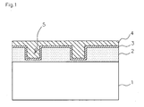
- Examples of a material to be polished which can be chemical mechanical polished by the process for chemical mechanical polishing of the present invention include a semiconductor substrate obtained by forming a trench part on an insulating layer stacked on a substrate such as a silicon wafer and, depositing a metal as a wiring material on the whole surface of the substrate with a trench on which a barrier metal layer has been formed thereafter, and the like.
- Examples of a metal constituting the wiring include copper, tungsten, aluminum and the like, and the present can be particularly suitably employed when the material is copper.
- copper includes, in addition to pure copper, an alloy of copper and silicon, an alloy of copper and aluminum, and an alloy containing copper at 95% by weight or more.
- examples of a material constituting the barrier metal layer include tantalum, tantalum nitride, titanium, titanium nitride and the like.
- tantalum is not limited to pure tantalum but includes an alloy containing tantalum such as tantalum-niobium and the like.
- tantalum nitride, titanium and titanium nitride are not limited to pure product.
- the process for chemical mechanical polishing of the present invention can suppress a surface defect such as occurrence of scratches and the like even when an insulating layer having a low dielectric constant is used as a material to be polished. Since an insulating layer having a low dielectric constant is weaker in the mechanical strength as compared with the conventional SiO 2 layer, when chemical mechanical polishing is performed by the previously known process for chemical mechanical polishing, the surface defect such as scratch and the like easily occurs, but according to the process for chemical mechanical polishing of the present invention, the better surface state can be obtained even when such an insulating layer having a low dielectric constant is polished.
- the process for chemical mechanical polishing of the present invention can be suitably applied even when an insulating layer having a low dielectric constant and having a modulus of 20GPa or less as measured by a nanoindentation method as the material constituting an insulating layer is polished.
- the modules may be 10GPa or less, particularly 5GPa or less.
- This modulus can be obtained by employing a nanoindenter "UMIS-2000" (trade name) manufactured by CSIRO described in the item of 4.1 nanoindenter of 4. principle and application of nanoindentation, in "Principle and Application of Nanoindentation Method", page 358-363, Non-Destructive Inspection, vol.47, No.6(1998), by the method described in the item of 4.2 a nanoindentation method using an acute angle indenter, or the method described in 4.3 a nanoindentation method using a hemispherical-shaped indenter.
- UMIS-2000 trade name
- Examples of the insulating layer having a low dielectric constant include:
- examples of the insulating layer comprised mainly of silsesquioxane include a porous layer having a density of 0.3 to 1.85g/cm 3 and having fine air bubbles of a hole diameter of 100nm or less.
- the semiconductor substrate is that a barrier metal layer is formed between the metal layer as the wiring material and the insulating layer
- the insulating layer part is ideally not chemical mechanical polished.
- excess polishing meaning that polishing is continued longer than a time calculated to be necessary for removing a metal layer
- a material constituting the insulating layer is partially exposed on the surface to be polished in some cases and, in such case, a surface defect such as scratch is generated.
- the process for chemical mechanical polishing of the present invention has advantages that a surface defect such as scratch is suppressed and a yield of products is improved, even when a mechanical fragile material of a low dielectric constant is used as a material constituting an insulating layer.
- the process for chemical mechanical polishing of the invention leads to an effective suppression of a phenomenon that the insulating layer having a low dielectric constant as a lower layer peels from its periphery during polishing at a step where the insulating layer having a low dielectric constant is not exposed on the polishing surface, that is, at a step where only a metal layer as a wiring material is chemically mechanical polished.
- This effect is presumed to be due to setting of a frictional force between a polishing pad and a metal layer (preferably copper layer) as a material to be polished, in an appropriate range.
- a value of driving current of a polishing table upon chemical mechanical polishing can be used as a substitute as described above, and the driving current in this case should be understood as being a driving current at a step where a metal layer (preferably copper layer) is chemical mechanical polished.
- a fumed silica particle (trade name; "Aerosil #50" manufactured by Nippon Aerosil Co., Ltd.) was placed in 6.7kg of ion-exchanged water, dispersed therein with an ultrasonic disperser, filtered with a filter having a pore diameter of 5 ⁇ m to prepare a dispersion containing a fumed silica particle.
- An average primary particle diameter of the fumed silica particle contained in this dispersion was 20nm, and an average secondary particle diameter was 200nm.
- a dispersion containing a fumed alumina particle was prepared similarly to above 1-1 except for exchanging the fumed silica particle for a fumed alumina particle (trade name; "Aluminum Oxide C” manufactured by Degussa Co., Ltd.).
- An average primary particle diameter of the fumed alumina particle contained in this dispersion was 13nm. and an average secondary particle diameter was 130nm.
- methyl methacrylate 5 parts by weight of methoxy polyethylene glycol methacrylate (trade name; "NK Ester M-90G #400” manufactured by Shin-Nakamura Chemical Co., Ltd.), 5 parts by weight of 4-vinylpyridine, 2 parts by weight of an azo-based polymerization initiator (trade name; "V50” manufactured by Wako Pure Chemical Industries, Ltd.) and 400 parts by weight of ion-exchanged water were placed in a flask having a volume of 2 liter, a temperature of the mixture was raised to 70°C while stirring in the nitrogen gas atmosphere, to perform polymerization for 6 hours.
- methoxy polyethylene glycol methacrylate trade name; "NK Ester M-90G #400” manufactured by Shin-Nakamura Chemical Co., Ltd.
- 4-vinylpyridine 2 parts by weight of an azo-based polymerization initiator (trade name; "V50” manufactured by Wako Pure Chemical Industries, Ltd.) and 400 parts by weight of ion-ex
- a dispersion containing a polymethyl methacrylate-based particle which has a positive ion of an amino group and a polyethylene glycol chain and has an average particle diameter of 0.15 ⁇ m was obtained.
- Ion-exchanged water was added to this dispersion containing a polymethyl methacrylate-based particle, to adjust the content of the particle to 10% by weight.
- a polymerization yield was 95%.
- this dispersion containing the polymethyl methacrylate-based particle (the particle content is 10% by weight) was placed in a flask having a volume of 2 liter, 1 part by weight of methyl trimethoxysilane was added, and the mixture was stirred at 40°C for 2 hours. Thereafter, pH was adjusted to 2 with 1N nitric acid to obtain a dispersion (a).
- the zeta potential of a polymethyl methacrylate-based particle containing in the dispersion (a) was +17mV.
- pH of a dispersion containing 10% by weight of a colloidal silica (trade name; "Snowtex O” manufactured by Nissan Chemical Co., Ltd.) (an average primary particle diameter of contained colloidal silica is 12nm, and an average secondary particle diameter is 79nm) was adjusted to 8 with 1N potassium hydroxide solution, to obtain a dispersion (b).
- the zeta potential of a colloidal silica particle contained in the dispersion (b) was -40mV.
- dispersion (b) 50 parts by weight of the dispersion (b) was slowly added to 100 parts by weight of the dispersion (a) over 2 hours to mix them, and the mixture was stirred for 2 hours to obtain a dispersion containing a particle in which the silica particle was attached to polymethyl methacrylate-based particle.
- pH of the mixed dispersion became 6.5
- the zeta potential of the polymethyl methacrylate-based particle was +6.5mV
- the zeta potential of the colloidal silica particle was -30mV, at this pH.
- a predetermined amount of the dispersion containing a fumed silica particle prepared in the above 1-1 was placed in a polyethylene bottle and, additives described in Table 1 were added according to the content (% by weight) described in Table 1, and then the mixture was sufficiently stirred.
- a hydrogen peroxide 31% by weight of aqueous hydrogen peroxide was employed, and an amount thereof was as described in Table 1 in terms of pure hydrogen peroxide.
- DBK denotes potassium dodecylbenzenesulfonate.
- the pH of the chemical mechanical aqueous dispersion [1] was 10.5.
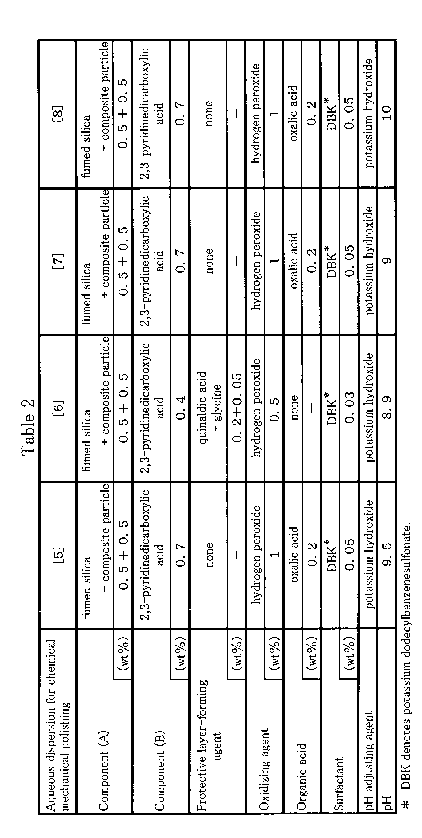
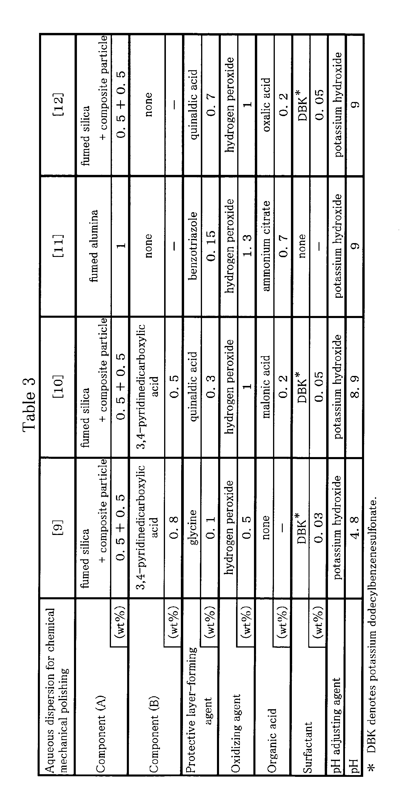
- Aqueous dispersions [2] to [12] were prepared similarly to the above aqueous dispersion [1] except using a kind and an amount of respective components to be incorporated, a pH adjusting agent and pH described in Table 1 to Table 3.
- aqueous dispersions [3] to [10] and [12] For the preparation of aqueous dispersions [3] to [10] and [12], a dispersion containing a fumed silica particle prepared in the above 1-1 and a dispersion containing a composite particle prepared in the above 1-3 are used. A predetermined amount of them were successively placed in a container to resulting dispersions. For the aqueous dispersion [6], quinaldinic acid and glycine were incorporated by successively adding them at each predetermined amount.
- ammonia which is a pH adjusting agent for the aqueous dispersions [7] and [8]
- 28% by weight of aqueous ammonia was employed at an amount described in Table 2 in terms of pure ammonia.
- DBK denotes potassium dodecylbenzenesulfonate
- Polishing performances of a copper film and an insulating layer were evaluated by using the aqueous dispersions [1] to [12] prepared as described above.
- a mixed solution containing 101.5g of methyltrimethoxysilane, 276.8g of methyl methoxypropionate and 9.7g of tetraisopropoxy titanium / ethyl acetoacetate complex was heated to 60°C, and a mixture of 112.3g of ⁇ -butyrolactone and water (4.58:1 by weight ratio) was added dropwise to this mixed solution for 1 hour. After completion of addition of the mixture, the mixture was reacted at 60°C for 1 hour to obtain a polysiloxane sol.
- styrene particles 100 parts by weight of styrene, 2 parts by weight of azo-based polymerization initiator (trade name; "V60” manufactured by Wako Pure Chemical Industries, Ltd.), 0.5 part by weight of potassium dodecylbenzenesulfonate and 400 parts by weight of ion-exchanged water were placed in a flask, and a temperature was raised to 70°C while stirring under the nitrogen gas atmosphere, to perform polymerization for 6 hours. Thereby, a polystyrene particle having an average particle diameter of 150nm was obtained.
- a cross-section of the cured film was observed with a scanning electron microscope, and a formation of fine pores was observed.
- a specific dielectric constant was 1.98
- a modulus was 3GPa by a nanoindentation method
- a void rate was 15%.
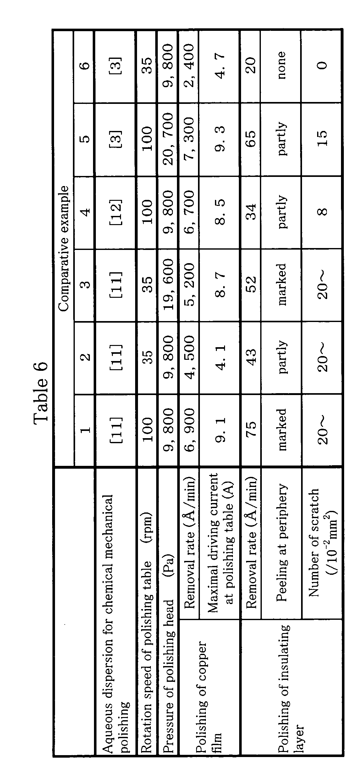
- the removal rate of the insulating layer having a low dielectric constant, the presence or not of peeling at a periphery and the number of scratches per unit area are shown in Tables 4 to 6.
- the object of the present invention is to provide a process for chemical mechanical polishing of semiconductor substrate that is particularly useful for chemical mechanical polishing a wafer having a wiring pattern and an insulating layer having a low dielectric constant is formed between wiring patterns, interlayers in the case of a multi-layer wiring and the like in the process of producing a semiconductor device, and an aqueous dispersion for chemical mechanical polishing which is used in this process.
- the process for chemical mechanical polishing of a semiconductor substrate of the present invention is that a surface to be polished of the semiconductor substrate is polished under conditions of a rotation speed of a polishing table fixing a polishing pad at the range from 50 to 200 rpm and a pressing pressure of the semiconductor substrate fixed to a polishing head against a polishing pad at the range from 700 to 18,000Pa, by using an aqueous dispersion for chemical mechanical polishing comprising an abrasive and at least one compound selected from the group consisting of polycarboxylic acid having a heterocycle and anhydride thereof, and the polishing pad.
Landscapes
- Chemical & Material Sciences (AREA)
- Organic Chemistry (AREA)
- Mechanical Treatment Of Semiconductor (AREA)
- Finish Polishing, Edge Sharpening, And Grinding By Specific Grinding Devices (AREA)
Abstract
Description



Claims (6)
- A process for chemical mechanical polishing of a semiconductor substrate characterized in that a surface to be polished of said semiconductor substrate is polished under conditions of a rotation speed of a polishing table fixing a polishing pad at the range from 50 to 200 rpm and a pressing pressure of said semiconductor substrate fixed to a polishing head against said polishing pad at the range from 700 to 18,000Pa, by using an aqueous dispersion for chemical mechanical polishing comprising (A) an abrasive and (B) at least one compound selected from the group consisting of polycarboxylic acid having a heterocycle and anhydride thereof, and said polishing pad.
- The process for chemical mechanical polishing of a semiconductor substrate according to Claim 1, wherein said abrasive (A) is comprised of at least one kind of particle selected from the group consisting of an inorganic particle and an organic particle, and an organic-inorganic composite particle.
- The process for chemical mechanical polishing of a semiconductor substrate according to Claim 1 or 2, wherein said polycarboxylic acid having a heterocycle and anhydride thereof (B) is at least one compound selected from the group consisting of 2,3-pyridinedicarboxylic acid, 2,3-pyridinedicarboxylic anhydride, 2,5-pyridinedicarboxylic acid, 2.6-pyridinedicarboxylic acid, 3,4-pyridinedicarboxylic acid, 3,5-pyridinedicarboxylic acid, 1-(1', 2'-dicarboxyethyl)benzotriazole, 4,4'-dicarboxy-2,2'-bipyridine and 5,5'-dicarboxy-2,2'-bipyridine.
- The process for chemical mechanical polishing of a semiconductor substrate according to any one of Claims 1 to 3, wherein said surface to be polished has at least one selected from the group consisting of a copper layer and an insulating layer.
- The process for chemical mechanical polishing of a semiconductor substrate according to Claim 4, wherein said insulating layer has a modulus of 20GPa or less measured by a nanoindentation method.
- An aqueous dispersion for chemical mechanical polishing comprising (A) an abrasive and (B) at least one compound selected from the group consisting of polycarboxylic acid having a heterocycle and anhydride thereof, wherein said dispersion is used for polishing a surface to be polished of said semiconductor substrate with a polishing pad, under conditions of a rotation speed of a polishing table fixing a polishing pad at the range from 50 to 200 rpm and a pressing pressure of said semiconductor substrate fixed to a polishing head against said polishing pad at the range from 700 to 18,000Pa.
Applications Claiming Priority (4)
| Application Number | Priority Date | Filing Date | Title |
|---|---|---|---|
| JP2002016701 | 2002-01-25 | ||
| JP2002016701 | 2002-01-25 | ||
| JP2002293223 | 2002-10-07 | ||
| JP2002293223A JP4187497B2 (en) | 2002-01-25 | 2002-10-07 | Chemical mechanical polishing method for semiconductor substrate |
Publications (2)
| Publication Number | Publication Date |
|---|---|
| EP1333476A2 true EP1333476A2 (en) | 2003-08-06 |
| EP1333476A3 EP1333476A3 (en) | 2005-10-19 |
Family
ID=26625636
Family Applications (1)
| Application Number | Title | Priority Date | Filing Date |
|---|---|---|---|
| EP03001656A Ceased EP1333476A3 (en) | 2002-01-25 | 2003-01-24 | Process for chemical mechanical polishing of semiconductor substrate and aqueous dispersion for chemical mechanical polishing |
Country Status (6)
| Country | Link |
|---|---|
| US (1) | US7183211B2 (en) |
| EP (1) | EP1333476A3 (en) |
| JP (1) | JP4187497B2 (en) |
| KR (1) | KR100801402B1 (en) |
| CN (1) | CN1300828C (en) |
| TW (1) | TWI257420B (en) |
Cited By (13)
| Publication number | Priority date | Publication date | Assignee | Title |
|---|---|---|---|---|
| GB2397580A (en) * | 2002-12-26 | 2004-07-28 | Kao Corp | Microwaviness reducing agent and polishing composition |
| EP1386949B1 (en) * | 2002-08-02 | 2009-01-14 | JSR Corporation | Use of an aqueous dispersion for chemical mechanical polishing and process for producing a semiconductor device |
| US7968884B2 (en) | 2006-12-05 | 2011-06-28 | Semiconductor Energy Laboratory Co., Ltd. | Semiconductor device and manufacturing method thereof |
| US8067772B2 (en) | 2006-12-05 | 2011-11-29 | Semiconductor Energy Laboratory Co., Ltd. | Semiconductor device and manufacturing method thereof |
| EP2418259A1 (en) * | 2003-09-30 | 2012-02-15 | Fujimi Incorporated | Polishing composition |
| US8476744B2 (en) | 2009-12-28 | 2013-07-02 | Semiconductor Energy Laboratory Co., Ltd. | Thin film transistor with channel including microcrystalline and amorphous semiconductor regions |
| US8575608B2 (en) | 2009-12-21 | 2013-11-05 | Semiconductor Energy Laboratory Co., Ltd. | Thin film transistor and manufacturing method thereof |
| US8704230B2 (en) | 2010-08-26 | 2014-04-22 | Semiconductor Energy Laboratory Co., Ltd. | Semiconductor device and manufacturing method thereof |
| US8829522B2 (en) | 2009-12-21 | 2014-09-09 | Semiconductor Energy Laboratory Co., Ltd. | Thin film transistor |
| US9230826B2 (en) | 2010-08-26 | 2016-01-05 | Semiconductor Energy Laboratory Co., Ltd. | Etching method using mixed gas and method for manufacturing semiconductor device |
| TWI557195B (en) * | 2008-06-11 | 2016-11-11 | Shinetsu Chemical Co | Synthetic quartz glass substrate with abrasive |
| US10214663B2 (en) | 2014-08-11 | 2019-02-26 | St. Lawrence Nanotechnology | Chemical-mechanical polishing composition comprising organic/inorganic composite particles |
| CN114829538A (en) * | 2019-12-26 | 2022-07-29 | 霓达杜邦股份有限公司 | Slurry for polishing |
Families Citing this family (36)
| Publication number | Priority date | Publication date | Assignee | Title |
|---|---|---|---|---|
| US7524346B2 (en) * | 2002-01-25 | 2009-04-28 | Dupont Air Products Nanomaterials Llc | Compositions of chemical mechanical planarization slurries contacting noble-metal-featured substrates |
| US20040188387A1 (en) * | 2003-03-25 | 2004-09-30 | Brask Justin K. | Removing silicon nano-crystals |
| TWI292931B (en) * | 2003-05-12 | 2008-01-21 | Jsr Corp | Chemical mechanical polishing agent kit and chemical mechanical polishing method using the same |
| JP2004342751A (en) * | 2003-05-14 | 2004-12-02 | Toshiba Corp | Slurry for CMP, polishing method, and method for manufacturing semiconductor device |
| TWI241626B (en) | 2003-06-02 | 2005-10-11 | Toshiba Corp | Chemical mechanical polishing method of organic film and method of manufacturing semiconductor device |
| TWI291987B (en) * | 2003-07-04 | 2008-01-01 | Jsr Corp | Chemical mechanical polishing aqueous dispersion and chemical mechanical polishing method |
| JP2005116987A (en) * | 2003-10-10 | 2005-04-28 | Fujimi Inc | Polishing composition |
| JP2005268666A (en) * | 2004-03-19 | 2005-09-29 | Fujimi Inc | Polishing composition |
| US7504044B2 (en) * | 2004-11-05 | 2009-03-17 | Cabot Microelectronics Corporation | Polishing composition and method for high silicon nitride to silicon oxide removal rate ratios |
| US7531105B2 (en) * | 2004-11-05 | 2009-05-12 | Cabot Microelectronics Corporation | Polishing composition and method for high silicon nitride to silicon oxide removal rate ratios |
| JP2006165142A (en) * | 2004-12-06 | 2006-06-22 | Jsr Corp | Chemical mechanical polishing aqueous dispersion and chemical mechanical polishing method |
| WO2006078074A2 (en) | 2005-01-24 | 2006-07-27 | Showa Denko K.K. | Polishing composition and polishing method |
| JP2007266507A (en) * | 2006-03-29 | 2007-10-11 | Fujifilm Corp | Polishing method |
| TWI437083B (en) * | 2006-07-28 | 2014-05-11 | 昭和電工股份有限公司 | Abrasive composition |
| US20080122107A1 (en) * | 2006-09-22 | 2008-05-29 | Taiwan Semiconductor Manufacturing Co., Ltd. | Poly silicon hard mask |
| JP4143872B2 (en) * | 2006-10-06 | 2008-09-03 | Jsr株式会社 | Chemical mechanical polishing aqueous dispersion and semiconductor device chemical mechanical polishing method |
| US9343330B2 (en) * | 2006-12-06 | 2016-05-17 | Cabot Microelectronics Corporation | Compositions for polishing aluminum/copper and titanium in damascene structures |
| JP5327427B2 (en) | 2007-06-19 | 2013-10-30 | Jsr株式会社 | Chemical mechanical polishing aqueous dispersion preparation set, chemical mechanical polishing aqueous dispersion preparation method, chemical mechanical polishing aqueous dispersion, and chemical mechanical polishing method |
| KR20100065333A (en) * | 2007-08-23 | 2010-06-16 | 니타 하스 인코포레이티드 | Polishing composition |
| US7923507B2 (en) * | 2007-08-30 | 2011-04-12 | Siovation, Llc | Polyorganosiloxane—containing compositions |
| JP2009065001A (en) * | 2007-09-07 | 2009-03-26 | Jsr Corp | Chemical mechanical polishing aqueous dispersion, kit for preparing the dispersion, and method for preparing chemical mechanical polishing aqueous dispersion |
| JP5178121B2 (en) * | 2007-09-28 | 2013-04-10 | 富士フイルム株式会社 | Polishing liquid and polishing method |
| JP5121432B2 (en) * | 2007-12-11 | 2013-01-16 | キヤノン株式会社 | Liquid crystal display device, manufacturing method thereof, and liquid crystal projection device |
| CN103342986B (en) | 2008-12-11 | 2015-01-07 | 日立化成株式会社 | Polishing solution for CMP and polishing method using same |
| JP5371416B2 (en) * | 2008-12-25 | 2013-12-18 | 富士フイルム株式会社 | Polishing liquid and polishing method |
| JP2009302551A (en) * | 2009-08-05 | 2009-12-24 | Jsr Corp | Set for manufacturing water-based dispersing element for chemical-mechanical polishing |
| JP5648567B2 (en) * | 2010-05-07 | 2015-01-07 | 日立化成株式会社 | Polishing liquid for CMP and polishing method using the same |
| US9318339B2 (en) * | 2011-10-13 | 2016-04-19 | Mitsui Mining & Smelting, Ltd | Polishing slurry and polishing method |
| US20130189843A1 (en) * | 2012-01-24 | 2013-07-25 | You Wang | Slurry for planarizing photoresist |
| JP5400228B1 (en) | 2012-04-27 | 2014-01-29 | 三井金属鉱業株式会社 | SiC single crystal substrate |
| KR101526006B1 (en) * | 2012-12-31 | 2015-06-04 | 제일모직주식회사 | Cmp slurry composition for copper and polishing method using the same |
| JP6156630B2 (en) * | 2013-05-24 | 2017-07-05 | Jsr株式会社 | Chemical mechanical polishing aqueous dispersion and chemical mechanical polishing method |
| KR102543680B1 (en) * | 2015-12-17 | 2023-06-16 | 솔브레인 주식회사 | Slurry composition for chemical mechanical polishing |
| US10259099B2 (en) * | 2016-08-04 | 2019-04-16 | Rohm And Haas Electronic Materials Cmp Holdings, Inc. | Tapering method for poromeric polishing pad |
| CN108117838B (en) * | 2016-11-29 | 2021-09-17 | 安集微电子科技(上海)股份有限公司 | Silicon nitride chemical mechanical polishing solution |
| CN108857860A (en) * | 2018-06-12 | 2018-11-23 | 宁波江丰电子材料股份有限公司 | Grinding method, wafer orientation ring and its application of wafer orientation ring and chemical mechanical polishing apparatus |
Family Cites Families (25)
| Publication number | Priority date | Publication date | Assignee | Title |
|---|---|---|---|---|
| WO1996013798A2 (en) * | 1994-10-25 | 1996-05-09 | United Parcel Service Of America, Inc. | Automatic electronic camera for label image capture |
| US5982916A (en) * | 1996-09-30 | 1999-11-09 | Siemens Corporate Research, Inc. | Method and apparatus for automatically locating a region of interest in a radiograph |
| US6309560B1 (en) | 1996-12-09 | 2001-10-30 | Cabot Microelectronics Corporation | Chemical mechanical polishing slurry useful for copper substrates |
| JP3371775B2 (en) * | 1997-10-31 | 2003-01-27 | 株式会社日立製作所 | Polishing method |
| US6556708B1 (en) * | 1998-02-06 | 2003-04-29 | Compaq Computer Corporation | Technique for classifying objects within an image |
| EP1102821A4 (en) | 1998-06-10 | 2004-05-19 | Rodel Inc | COMPOSITION AND METHOD FOR CHEMICAL / MECHANICAL POLISHING |
| CN100381537C (en) | 1998-08-31 | 2008-04-16 | 日立化成工业株式会社 | Metal grinding liquid and grinding method |
| JP2000183003A (en) * | 1998-10-07 | 2000-06-30 | Toshiba Corp | Polishing composition for copper-based metal and method for manufacturing semiconductor device |
| ATE474899T1 (en) * | 1998-10-23 | 2010-08-15 | Fujifilm Electronic Materials | A CHEMICAL-MECHANICAL POLISHING SLURRY CONTAINING AN ACCELERATOR SOLUTION |
| KR100447551B1 (en) | 1999-01-18 | 2004-09-08 | 가부시끼가이샤 도시바 | Composite Particles and Production Process Thereof, Aqueous Dispersion, Aqueous Dispersion Composition for Chemical Mechanical Polishing, and Process for Manufacture of Semiconductor Apparatus |
| JP4041236B2 (en) | 1999-01-18 | 2008-01-30 | 株式会社東芝 | Composite particle for chemical mechanical polishing used for manufacturing semiconductor device, method for manufacturing the same, and chemical mechanical polishing method using the same |
| EP1036836B1 (en) | 1999-03-18 | 2004-11-03 | Kabushiki Kaisha Toshiba | Aqueous dispersion for chemical mechanical polishing |
| JP3857474B2 (en) | 1999-10-08 | 2006-12-13 | 株式会社東芝 | Aqueous dispersion for chemical mechanical polishing |
| JP4657408B2 (en) | 1999-10-13 | 2011-03-23 | 株式会社トクヤマ | Metal film abrasive |
| JP2001127027A (en) | 1999-10-27 | 2001-05-11 | Hitachi Chem Co Ltd | Metal polishing method |
| JP4151178B2 (en) | 1999-11-22 | 2008-09-17 | Jsr株式会社 | Process for producing aqueous dispersion for chemical mechanical polishing |
| JP4151179B2 (en) | 1999-11-22 | 2008-09-17 | Jsr株式会社 | Method for producing composite particles, composite particles produced by this method, and chemical mechanical polishing aqueous dispersion containing composite particles |
| WO2001044395A1 (en) * | 1999-12-14 | 2001-06-21 | Rodel Holdings, Inc. | Polishing compositions for semiconductor substrates |
| JP3805588B2 (en) * | 1999-12-27 | 2006-08-02 | 株式会社日立製作所 | Manufacturing method of semiconductor device |
| TW572980B (en) | 2000-01-12 | 2004-01-21 | Jsr Corp | Aqueous dispersion for chemical mechanical polishing and chemical mechanical polishing process |
| JP2001269859A (en) | 2000-03-27 | 2001-10-02 | Jsr Corp | Aqueous dispersion for chemical mechanical polishing |
| JP3837277B2 (en) | 2000-06-30 | 2006-10-25 | 株式会社東芝 | Chemical mechanical polishing aqueous dispersion for use in polishing copper and chemical mechanical polishing method |
| JP3825246B2 (en) * | 2000-11-24 | 2006-09-27 | Necエレクトロニクス株式会社 | Chemical mechanical polishing slurry |
| US20030104770A1 (en) * | 2001-04-30 | 2003-06-05 | Arch Specialty Chemicals, Inc. | Chemical mechanical polishing slurry composition for polishing conductive and non-conductive layers on semiconductor wafers |
| US6620215B2 (en) * | 2001-12-21 | 2003-09-16 | Dynea Canada, Ltd. | Abrasive composition containing organic particles for chemical mechanical planarization |
-
2002
- 2002-10-07 JP JP2002293223A patent/JP4187497B2/en not_active Expired - Fee Related
-
2003
- 2003-01-23 US US10/349,092 patent/US7183211B2/en not_active Expired - Fee Related
- 2003-01-24 CN CNB031033466A patent/CN1300828C/en not_active Expired - Fee Related
- 2003-01-24 TW TW092101622A patent/TWI257420B/en not_active IP Right Cessation
- 2003-01-24 KR KR1020030004696A patent/KR100801402B1/en not_active Expired - Fee Related
- 2003-01-24 EP EP03001656A patent/EP1333476A3/en not_active Ceased
Cited By (20)
| Publication number | Priority date | Publication date | Assignee | Title |
|---|---|---|---|---|
| EP1386949B1 (en) * | 2002-08-02 | 2009-01-14 | JSR Corporation | Use of an aqueous dispersion for chemical mechanical polishing and process for producing a semiconductor device |
| GB2397580A (en) * | 2002-12-26 | 2004-07-28 | Kao Corp | Microwaviness reducing agent and polishing composition |
| GB2397580B (en) * | 2002-12-26 | 2006-11-08 | Kao Corp | Polishing composition |
| US7553345B2 (en) | 2002-12-26 | 2009-06-30 | Kao Corporation | Polishing composition |
| EP2418259A1 (en) * | 2003-09-30 | 2012-02-15 | Fujimi Incorporated | Polishing composition |
| US7968884B2 (en) | 2006-12-05 | 2011-06-28 | Semiconductor Energy Laboratory Co., Ltd. | Semiconductor device and manufacturing method thereof |
| US8067772B2 (en) | 2006-12-05 | 2011-11-29 | Semiconductor Energy Laboratory Co., Ltd. | Semiconductor device and manufacturing method thereof |
| US8834989B2 (en) | 2006-12-05 | 2014-09-16 | Semiconductor Energy Laboratory Co., Ltd. | Semiconductor device and manufacturing method thereof |
| TWI557195B (en) * | 2008-06-11 | 2016-11-11 | Shinetsu Chemical Co | Synthetic quartz glass substrate with abrasive |
| US8829522B2 (en) | 2009-12-21 | 2014-09-09 | Semiconductor Energy Laboratory Co., Ltd. | Thin film transistor |
| US8575608B2 (en) | 2009-12-21 | 2013-11-05 | Semiconductor Energy Laboratory Co., Ltd. | Thin film transistor and manufacturing method thereof |
| US8476744B2 (en) | 2009-12-28 | 2013-07-02 | Semiconductor Energy Laboratory Co., Ltd. | Thin film transistor with channel including microcrystalline and amorphous semiconductor regions |
| US8704230B2 (en) | 2010-08-26 | 2014-04-22 | Semiconductor Energy Laboratory Co., Ltd. | Semiconductor device and manufacturing method thereof |
| US9230826B2 (en) | 2010-08-26 | 2016-01-05 | Semiconductor Energy Laboratory Co., Ltd. | Etching method using mixed gas and method for manufacturing semiconductor device |
| US9257561B2 (en) | 2010-08-26 | 2016-02-09 | Semiconductor Energy Laboratory Co., Ltd. | Semiconductor device and manufacturing method thereof |
| US10214663B2 (en) | 2014-08-11 | 2019-02-26 | St. Lawrence Nanotechnology | Chemical-mechanical polishing composition comprising organic/inorganic composite particles |
| CN114829538A (en) * | 2019-12-26 | 2022-07-29 | 霓达杜邦股份有限公司 | Slurry for polishing |
| EP4083162A4 (en) * | 2019-12-26 | 2023-08-23 | NITTA DuPont Incorporated | SPURRY FOR POLISHING |
| CN114829538B (en) * | 2019-12-26 | 2024-04-26 | 霓达杜邦股份有限公司 | Grinding slurry |
| US12203008B2 (en) | 2019-12-26 | 2025-01-21 | Nitta Dupont Incorporated | Polishing slurry |
Also Published As
| Publication number | Publication date |
|---|---|
| US7183211B2 (en) | 2007-02-27 |
| CN1434491A (en) | 2003-08-06 |
| CN1300828C (en) | 2007-02-14 |
| JP4187497B2 (en) | 2008-11-26 |
| KR100801402B1 (en) | 2008-02-05 |
| EP1333476A3 (en) | 2005-10-19 |
| TW200302267A (en) | 2003-08-01 |
| KR20030064326A (en) | 2003-07-31 |
| US20030153183A1 (en) | 2003-08-14 |
| JP2003289055A (en) | 2003-10-10 |
| TWI257420B (en) | 2006-07-01 |
Similar Documents
| Publication | Publication Date | Title |
|---|---|---|
| US7183211B2 (en) | Process for chemical mechanical polishing of semiconductor substrate and aqueous dispersion for chemical mechanical polishing | |
| EP1138733B1 (en) | Aqueous dispersion for chemical mechanical polishing of insulating films | |
| US8574330B2 (en) | Chemical mechanical polishing aqueous dispersion and chemical mechanical polishing method for semiconductor device | |
| US8470195B2 (en) | Chemical mechanical polishing aqueous dispersion preparation set, method of preparing chemical mechanical polishing aqueous dispersion, chemical mechanical polishing aqueous dispersion, and chemical mechanical polishing method | |
| EP1386949B1 (en) | Use of an aqueous dispersion for chemical mechanical polishing and process for producing a semiconductor device | |
| US6935928B2 (en) | Chemical mechanical polishing aqueous dispersion and chemical mechanical polishing method | |
| TWI441907B (en) | Chemical machinery grinding water dispersions and chemical mechanical grinding methods | |
| US6653267B2 (en) | Aqueous dispersion for chemical mechanical polishing used for polishing of copper | |
| TWI413678B (en) | Polishing liquid | |
| JP2001200242A (en) | Aqueous slurry | |
| IL195698A (en) | Compositions and methods for polishing silicon nitride materials | |
| KR20010078784A (en) | Aqueous dispersion for chemical mechanical polishing | |
| US20090078908A1 (en) | Polishing liquid | |
| JP2005158867A (en) | Set for preparing chemical mechanical polishing aqueous dispersions | |
| JP2002256256A (en) | Aqueous dispersion for chemical mechanical polishing | |
| JP2005026604A (en) | Aqueous dispersion for chemical mechanical polishing | |
| JP2004128475A (en) | Aqueous dispersion for chemical mechanical polishing and method for manufacturing semiconductor device | |
| JP2010161201A (en) | Chemical mechanical polishing aqueous dispersion, chemical mechanical polishing method using the same, and method of manufacturing chemical mechanical polishing aqueous dispersion | |
| JP2007266619A (en) | Chemical mechanical polishing method for semiconductor substrate and aqueous dispersion for chemical mechanical polishing | |
| TW202438613A (en) | Polishing agent, polishing method, method for manufacturing a semiconductor component, and additive liquid for polishing | |
| JP2009302551A (en) | Set for manufacturing water-based dispersing element for chemical-mechanical polishing | |
| WO2025023040A1 (en) | Polishing agent and method for producing same, method for producing polishing agent additive liquid, polishing method, and method for producing semiconductor component | |
| JP2006114729A (en) | Method for removing excess metal layer | |
| JP2005142489A (en) | CMP abrasive and substrate polishing method | |
| JP2008109025A (en) | Chemical mechanical polishing aqueous dispersion and semiconductor device chemical mechanical polishing method |
Legal Events
| Date | Code | Title | Description |
|---|---|---|---|
| PUAI | Public reference made under article 153(3) epc to a published international application that has entered the european phase |
Free format text: ORIGINAL CODE: 0009012 |
|
| AK | Designated contracting states |
Designated state(s): AT BE BG CH CY CZ DE DK EE ES FI FR GB GR HU IE IT LI LU MC NL PT SE SI SK TR |
|
| AX | Request for extension of the european patent |
Extension state: AL LT LV MK RO |
|
| RAP1 | Party data changed (applicant data changed or rights of an application transferred) |
Owner name: JSR CORPORATION |
|
| PUAL | Search report despatched |
Free format text: ORIGINAL CODE: 0009013 |
|
| AK | Designated contracting states |
Kind code of ref document: A3 Designated state(s): AT BE BG CH CY CZ DE DK EE ES FI FR GB GR HU IE IT LI LU MC NL PT SE SI SK TR |
|
| AX | Request for extension of the european patent |
Extension state: AL LT LV MK RO |
|
| 17P | Request for examination filed |
Effective date: 20051117 |
|
| AKX | Designation fees paid |
Designated state(s): DE FR IT |
|
| 17Q | First examination report despatched |
Effective date: 20070102 |
|
| STAA | Information on the status of an ep patent application or granted ep patent |
Free format text: STATUS: THE APPLICATION HAS BEEN REFUSED |
|
| 18R | Application refused |
Effective date: 20150402 |