EP1333444A1 - Two transistor ferroelectric non-volatile memory - Google Patents
Two transistor ferroelectric non-volatile memory Download PDFInfo
- Publication number
- EP1333444A1 EP1333444A1 EP02258065A EP02258065A EP1333444A1 EP 1333444 A1 EP1333444 A1 EP 1333444A1 EP 02258065 A EP02258065 A EP 02258065A EP 02258065 A EP02258065 A EP 02258065A EP 1333444 A1 EP1333444 A1 EP 1333444A1
- Authority
- EP
- European Patent Office
- Prior art keywords
- ferroelectric
- transistor
- capacitor
- mos
- mos transistor
- Prior art date
- Legal status (The legal status is an assumption and is not a legal conclusion. Google has not performed a legal analysis and makes no representation as to the accuracy of the status listed.)
- Granted
Links
- 230000015654 memory Effects 0.000 title claims abstract description 77
- 239000003990 capacitor Substances 0.000 claims abstract description 83
- 238000000034 method Methods 0.000 claims description 5
- 230000005283 ground state Effects 0.000 abstract 1
- 230000014759 maintenance of location Effects 0.000 description 10
- 230000028161 membrane depolarization Effects 0.000 description 6
- 230000001066 destructive effect Effects 0.000 description 3
- 230000010287 polarization Effects 0.000 description 3
- 230000003542 behavioural effect Effects 0.000 description 1
- 230000005684 electric field Effects 0.000 description 1
- 230000001747 exhibiting effect Effects 0.000 description 1
- 239000003574 free electron Substances 0.000 description 1
- 230000007787 long-term memory Effects 0.000 description 1
- 238000004519 manufacturing process Methods 0.000 description 1
- 239000000463 material Substances 0.000 description 1
- 238000012986 modification Methods 0.000 description 1
- 230000004048 modification Effects 0.000 description 1
- 238000012856 packing Methods 0.000 description 1
- 239000007787 solid Substances 0.000 description 1
Images




Classifications
-
- G—PHYSICS
- G11—INFORMATION STORAGE
- G11C—STATIC STORES
- G11C11/00—Digital stores characterised by the use of particular electric or magnetic storage elements; Storage elements therefor
- G11C11/21—Digital stores characterised by the use of particular electric or magnetic storage elements; Storage elements therefor using electric elements
- G11C11/22—Digital stores characterised by the use of particular electric or magnetic storage elements; Storage elements therefor using electric elements using ferroelectric elements
Definitions
- This invention relates to ferroelectric memory, non-volatile memory and embedded memory, and specifically to a two-transistor memory unit exhibiting long term memory retention and low power consumption.
- Flash memory is generally a single transistor memory cell, which may be fabricated in a high packing density array, but which requires high voltage and which has a relatively slow programming process.
- Electrically Erasable Programmable Read-Only Memory (EEPROM) is a programmable memory array which has similar structural and behavioral characteristics to a flash memory, but which may be selectively erased.
- a one-transistor one-capacitor ferroelectric random access memory (1T-1C FeRAM) device is similar to a dynamic RAM (DRAM), which has a destructive read-out.
- DRAM dynamic RAM
- the family of 1T FeRAMs is still under development. These devices exhibit high standby leakage current and a low memory retention time, which are the two major obstacles of this family of memories.
- a two transistor ferroelectric non-volatile memory includes a ferroelectric capacitor having an upper electrode and a lower electrode, wherein the upper electrode is connected to a word line; a first MOS transistor includes a MOS linear capacitor located at a gate oxide region thereof, wherein a gate of the first MOS transistor is connected to the lower electrode of the ferroelectric capacitor and wherein a drain of the first MOS transistor is connected to a bit line and wherein the source of the first MOS transistor is connected to a ground; a second MOS transistor having a gate connected to a programming line, a drain connected to the lower electrode of the ferroelectric capacitor, and a source connected to a ground and the source of the first MOS transistor; wherein, when a positive pulse is applied to the word line and to the programming line, the second MOS transistor is switched on and connects the bottom electrode of the ferroelectric capacitor to the ground, a charge is placed on the ferroelectric capacitor thereby creating a "1" state in the memory.
- the second MOS transistor When a negative pulse is applied to the word line and a positive pulse is applied to the programming line, the second MOS transistor is switched on and connects the bottom electrode of the ferroelectric capacitor to the ground, a charge is placed on the ferroelectric capacitor, thereby creating a "0" state in the memory,
- Another object of the invention is to provide a FeRAM having both long memory retention characteristics and low power requirements.
- a further object of the invention is to provide a 2T-1C FeRAM.
- the present invention includes a 2T FeRAM, which solves both the high standby leakage current and the low memory retention time problems of 1T FeRAMs, and which exhibits a non-destructive read out.
- Fig. 1 depicts a 2T FeRAM constructed according to the invention, generally at 10.
- FeRAM 10 includes a first MOS transistor 12, a second MOS transistor 14, and a ferroelectric capacitor 16, which has a bottom electrode connected to a gate 12g of first MOS transistor 12 and to a drain 14d of second MOS transistor 14.
- a linear capacitor 18 is located at the gate oxide of first MOS transistor 12.
- ferroelectric capacitor 16 is connected to gate 12g of first, or cell, transistor 12.
- Second transistor 14 is the programming transistor.
- the drain 14d of second MOS transistor 14 is connected to the bottom electrode of ferroelectric capacitor 16 and the gate electrode 12g of cell transistor 12.
- a word line (WL) is connected to the top electrode of ferroelectric capacitor 16.
- a programming line (PL) is connected to the gate 14g of second MOS transistor 14, and a bit line (BL) is connected to the drain 12d of first MOS transistor 12, also referred to herein as a memory transistor.
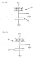
- Fig. 2a depicts the 2T FeRAM of the invention in a "0" state
- Fig. 2b depicts the 2T FeRAM in a "1" state during the programming.
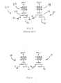
- FIG. 3 a prior art 1T ferroelectric memory is depicted schematically generally at 20.
- a MOS linear capacitor 22 is formed in series with a ferroelectric capacitor 24.
- a voltage is dropped across capacitors 22, 24.
- the amount of charge on ferroelectric capacitor 24 and MOS linear capacitor 22 are the same.
- the electric fields across the ferroelectric and MOS linear capacitors are in the same direction.
- the programming voltage drops to zero (right side of figure).
- the voltage created by the free charges on the MOS linear capacitor acts as a battery for the ferroelectric capacitor.
- the voltage however, is opposite to that of the polarization direction, and it is therefore called a "depolarization voltage.”
- the depolarization voltage quickly reverses the polarization, and the ferroelectric "memory" disappears.
- 2T FeRAM 10 is depicted at the beginning of its programming cycle.
- a positive pulse is applied to WL and to PL.
- Second transistor 14 is switched on and connects the bottom electrode of ferroelectric capacitor 16 to ground, thereby decoupling ferroelectric capacitor 16 from linear capacitor 18.
- the WL voltage is dropped only across the ferroelectric capacitor. This reduces the programming voltage, as comparing to the 1T ferroelectric memory of Fig. 3.
- the free electrons 15 in ferroelectric capacitor 16 are discharged. There is no depolarization voltage on ferroelectric capacitor 16, resulting in a long retention time for the 2T ferroelectric memory.
- a similar scheme is followed to write the memory to a "1" state.
- the reason for the long retention time of the memory device of the invention is that the MOS linear capacitor is decoupled from the ferroelectric capacitor and because both electrodes of ferroelectric capacitor 16 are at the same potential, i.e., the ground potential, after programming, and there is no de-polarization field across the ferroelectric material.
- the voltage across the ferroelectric capacitor, after programming is the de-polarization voltage: Q/(C ox + C fe ), where Q is the polarization charge, C ox is the gate oxide capacitance, the so-called linear, or constant, capacitor, and C fe is the capacitance of the ferroelectric capacitor.
- the memory transistor is off on both "1" and "0" states, even when V dd voltage is applied to the BL. Therefore, the 2T FeRAM of the invention has a low standby current
- a positive pulse on WL (center figure) charges the ferroelectric capacitor and the MOS linear capacitor. No domain switching occurs on the ferroelectric capacitor, however, the MOS linear capacitor is charged to Q linear 19. A low current may flow from the source (ground) to the drain (BL) of the memory transistor. After the reading cycle, the MOS linear capacitor charge Q linear is discharged, and the ferroelectric capacitor reverts to its original state.
- Fig. 8 depicts the reading process of the 2T FeRAM of the invention in a "1" state, wherein a positive pulse on WL (center figure) switches the ferroelectric domain and charges the MOS linear capacitor.
- a high current may flow from the source (ground) to the drain (BL) of the memory transistor because a strong inversion occurs on an nMOS memory transistor.
- the MOS linear capacitor generates a strong "depolarization field" which depolarizes the ferroelectric capacitor. This characteristic is similar to that of the 1T ferroelectric memory. In the case of the 2T FeRAM of the invention, however, the depolarization restores the memory back to its original state (right figure) and provides for a non-destructive read-out.
- a memory array of the invention is depicted generally at 30 in Fig. 9, and includes, in this depiction, four 2T FeRAM memory cells constructed according to the invention at 32, 34, 36 and 38.
Landscapes
- Engineering & Computer Science (AREA)
- Computer Hardware Design (AREA)
- Dram (AREA)
- Semiconductor Memories (AREA)
Abstract
Description
- This invention relates to ferroelectric memory, non-volatile memory and embedded memory, and specifically to a two-transistor memory unit exhibiting long term memory retention and low power consumption.
- A number of solid state, non-volatile memory devices are known in the art. Flash memory is generally a single transistor memory cell, which may be fabricated in a high packing density array, but which requires high voltage and which has a relatively slow programming process. Electrically Erasable Programmable Read-Only Memory (EEPROM) is a programmable memory array which has similar structural and behavioral characteristics to a flash memory, but which may be selectively erased. A one-transistor one-capacitor ferroelectric random access memory (1T-1C FeRAM) device is similar to a dynamic RAM (DRAM), which has a destructive read-out. The family of 1T FeRAMs is still under development. These devices exhibit high standby leakage current and a low memory retention time, which are the two major obstacles of this family of memories.
- Sung-Min Yoon et al., A novel FET-type Ferroelectric Memory with Excellent Data Retention Characteristics, describes a 1T-2C device wherein the data retention durations are enhanced by providing two ferroelectric capacitors, which are polarized in opposite directions, IEDM 2000.
- A two transistor ferroelectric non-volatile memory includes a ferroelectric capacitor having an upper electrode and a lower electrode, wherein the upper electrode is connected to a word line; a first MOS transistor includes a MOS linear capacitor located at a gate oxide region thereof, wherein a gate of the first MOS transistor is connected to the lower electrode of the ferroelectric capacitor and wherein a drain of the first MOS transistor is connected to a bit line and wherein the source of the first MOS transistor is connected to a ground; a second MOS transistor having a gate connected to a programming line, a drain connected to the lower electrode of the ferroelectric capacitor, and a source connected to a ground and the source of the first MOS transistor; wherein, when a positive pulse is applied to the word line and to the programming line, the second MOS transistor is switched on and connects the bottom electrode of the ferroelectric capacitor to the ground, a charge is placed on the ferroelectric capacitor thereby creating a "1" state in the memory. When a negative pulse is applied to the word line and a positive pulse is applied to the programming line, the second MOS transistor is switched on and connects the bottom electrode of the ferroelectric capacitor to the ground, a charge is placed on the ferroelectric capacitor, thereby creating a "0" state in the memory,
- It is an object of the invention to provide a FeRAM having non-volatile memory characteristics.
- Another object of the invention is to provide a FeRAM having both long memory retention characteristics and low power requirements.
- A further object of the invention is to provide a 2T-1C FeRAM.
- This summary and objectives of the invention are provided to enable quick comprehension of the nature of the invention. A more thorough understanding of the invention may be obtained by reference to the following detailed description of the preferred embodiment of the invention in connection with the drawings.
-
- Fig. 1 depicts the 2T FeRAM of the invention.
- Fig. 2 depicts the 2T FeRAM of the invention in "0" and "1" states
- Fig. 3 depicts a prior art 1T FeRAM at the beginning of a programming cycle.
- Fig. 4 depicts the 2T FeRAM of the invention at the beginning of a programming cycle.
- Fig. 5 depicts a prior art 1T FeRAM at the "1" and "0" states.
- Fig. 6 depicts the 2T FeRAM of the invention at the "1" and "0" states.
- Figs. 7 and 8 depict the 2T FeRAM of the invention during a read out operation.
- Fig. 9 depicts a memory array of 2T FeRAMs constructed according to the invention.
-
- The present invention includes a 2T FeRAM, which solves both the high standby leakage current and the low memory retention time problems of 1T FeRAMs, and which exhibits a non-destructive read out.
- As previously noted, the 1T ferroelectric memory exhibits several properties which need to be resolved in order to make 1T Fe devices suitable for user applications. The 2T ferroelectric memory cell of the invention solves the problems associated with 1T ferroelectric memory devices. Fig. 1 depicts a 2T FeRAM constructed according to the invention, generally at 10. FeRAM 10 includes a
first MOS transistor 12, asecond MOS transistor 14, and aferroelectric capacitor 16, which has a bottom electrode connected to a gate 12g offirst MOS transistor 12 and to a drain 14d ofsecond MOS transistor 14. Alinear capacitor 18 is located at the gate oxide offirst MOS transistor 12. - In the 2T FeRAM cell of the invention,
ferroelectric capacitor 16 is connected to gate 12g of first, or cell,transistor 12.Second transistor 14 is the programming transistor. The drain 14d ofsecond MOS transistor 14 is connected to the bottom electrode offerroelectric capacitor 16 and the gate electrode 12g ofcell transistor 12. A word line (WL) is connected to the top electrode offerroelectric capacitor 16. A programming line (PL) is connected to thegate 14g ofsecond MOS transistor 14, and a bit line (BL) is connected to thedrain 12d offirst MOS transistor 12, also referred to herein as a memory transistor. - Fig. 2a depicts the 2T FeRAM of the invention in a "0" state, while Fig. 2b depicts the 2T FeRAM in a "1" state during the programming.
- Turning to Fig. 3, a prior art 1T ferroelectric memory is depicted schematically generally at 20. A MOS
linear capacitor 22 is formed in series with aferroelectric capacitor 24. During the beginning of programming cycle (left portion of figure), a voltage is dropped acrosscapacitors ferroelectric capacitor 24 and MOSlinear capacitor 22 are the same. The electric fields across the ferroelectric and MOS linear capacitors are in the same direction. At the end of programming cycle, the programming voltage drops to zero (right side of figure). The voltage created by the free charges on the MOS linear capacitor acts as a battery for the ferroelectric capacitor. The voltage, however, is opposite to that of the polarization direction, and it is therefore called a "depolarization voltage." The depolarization voltage quickly reverses the polarization, and the ferroelectric "memory" disappears. - Referring now to Fig. 4,
2T FeRAM 10 is depicted at the beginning of its programming cycle. To programferroelectric memory cell 10 to a "0" state, a positive pulse is applied to WL and to PL.Second transistor 14 is switched on and connects the bottom electrode offerroelectric capacitor 16 to ground, thereby decouplingferroelectric capacitor 16 fromlinear capacitor 18. The WL voltage is dropped only across the ferroelectric capacitor. This reduces the programming voltage, as comparing to the 1T ferroelectric memory of Fig. 3. At the end of the programming cycle, thefree electrons 15 inferroelectric capacitor 16 are discharged. There is no depolarization voltage onferroelectric capacitor 16, resulting in a long retention time for the 2T ferroelectric memory. A similar scheme is followed to write the memory to a "1" state. - The reason for the long retention time of the memory device of the invention is that the MOS linear capacitor is decoupled from the ferroelectric capacitor and because both electrodes of
ferroelectric capacitor 16 are at the same potential, i.e., the ground potential, after programming, and there is no de-polarization field across the ferroelectric material. In the case of a 1T FeRAM memory cell of the prior art, the voltage across the ferroelectric capacitor, after programming, is the de-polarization voltage: Q/(Cox + Cfe), where Q is the polarization charge, Cox is the gate oxide capacitance, the so-called linear, or constant, capacitor, and Cfe is the capacitance of the ferroelectric capacitor. In the 2T FeRAM of the invention, a charge that is equal to the storage charge, but of opposite polarity, is induced into the bottom electrode of the ferroelectric capacitor. As a result, the net storage charge is about zero. There is no depolarization field across the ferroelectric capacitor, - Tumins now to Fig. 5, 1T
ferroelectric memory 20 is depicted after the device is written to the "1" state on the left side of the figure.Transistor 26 is turned on, and will stay on even after WL is turned off. When Vdd is applied to BL to address another memory cell, a current will flow onmemory cell 20, even though it is not being addressed. This results in reading noise and requires a higher standby power formemory 20. A selecting transistor to be incorporated into every ferroelectric memory cell has been proposed to address this problem in U.S. Patent No. 5,932,904, Two transistor ferroelectric memory cell, to Hsu et al., granted.August 3, 1999, and in U. S. Patent No. 6,146,904, for Method of making a two transistor ferroelectric memory cell, also to Hsu et al., granted November 14, 2000, however, the selecting transistor increases the memory cell size to a 2T configuration, as in this invention, without resolving the retention problem of the ferroelectric memory. - Referring to Fig. 6, in the case of 2T
ferroelectric memory cell 10, the memory transistor is off on both "1" and "0" states, even when Vdd voltage is applied to the BL. Therefore, the 2T FeRAM of the invention has a low standby current - Turning to Fig. 7, during a read cycle, positive pulses are applying to WL and BL, leaving PL "floating." In the case of the "0" state of the 2T ferroelectric memory cell of the invention, a positive pulse on WL (center figure) charges the ferroelectric capacitor and the MOS linear capacitor. No domain switching occurs on the ferroelectric capacitor, however, the MOS linear capacitor is charged to
Q linear 19. A low current may flow from the source (ground) to the drain (BL) of the memory transistor. After the reading cycle, the MOS linear capacitor charge Qlinear is discharged, and the ferroelectric capacitor reverts to its original state. - Fig. 8 depicts the reading process of the 2T FeRAM of the invention in a "1" state, wherein a positive pulse on WL (center figure) switches the ferroelectric domain and charges the MOS linear capacitor. A high current may flow from the source (ground) to the drain (BL) of the memory transistor because a strong inversion occurs on an nMOS memory transistor. At the end of read cycle, the MOS linear capacitor generates a strong "depolarization field" which depolarizes the ferroelectric capacitor. This characteristic is similar to that of the 1T ferroelectric memory. In the case of the 2T FeRAM of the invention, however, the depolarization restores the memory back to its original state (right figure) and provides for a non-destructive read-out.
- A memory array of the invention is depicted generally at 30 in Fig. 9, and includes, in this depiction, four 2T FeRAM memory cells constructed according to the invention at 32, 34, 36 and 38.
- Thus, a two transistor ferroelectric non-volatile memory has been disclosed. It will be appreciated that further variations and modifications thereof may be made within the scope of the invention as defined in the appended claims.
Claims (16)
- A two transistor ferroelectric non-volatile memory comprising:a ferroelectric capacitor connected to a word line and having an upper electrode and a lower electrode;a first MOS transistor having gate connected to the lower electrode of said ferroelectric capacitor, wherein a drain of said first MOS transistor is connected to a bit line, and wherein a source of said first MOS transistor is connected to a ground;a MOS linear capacitor located at the gate oxide of said first MOS transistor; anda second MOS transistor having a gate connected to a programming line, a drain connected to the lower electrode of said ferroelectric capacitor, and a source connected to a ground and said source of said first MOS transistor.
- The two transistor ferroelectric non-volatile memory of claim 1 wherein, when a positive pulse is applied to said word line and to said programming line, a charge is placed on said ferroelectric capacitor and said MOS linear capacitor, and wherein, after the positive pulse is applied, said ferroelectric capacitor is decoupled from said MOS linear capacitor, thereby creating a "1" state in the memory.
- The two transistor ferroelectric non-volatile memory of claim 1 wherein when a negative pulse is applied to the word line and a positive pulse is applied to the programming line, a "0" state is created.
- The two transistor ferroelectric non-volatile memory of claim 1 wherein said first MOS transistor is off on both "1" and "0" states, even when a voltage is applied to a bit line, thereby requiring a low standby current.
- The two transistor ferroelectric non-volatile memory of claim 1 wherein, during a reading process of the memory in a "1" state, a positive pulse on the word line switches the ferroelectric domain and charges the MOS linear capacitor.
- The two transistor ferroelectric non-volatile memory of claim 1 wherein, during a read-out cycle, the memory is read, and retains said charge on said ferroelectric capacitor.
- A two transistor ferroelectric non-volatile memory comprising:wherein, when a positive pulse is applied to said word line and to said programming line, a charge is placed on said ferroelectric capacitor and said ferroelectric capacitor is decoupled from said MOS linear capacitor, thereby creating a "1" state in the memory.a ferroelectric capacitor connected to a word line and having an upper electrode and a lower electrode;a first MOS transistor having gate connected to the lower electrode of said ferroelectric capacitor, wherein a drain of said first MOS transistor is connected to a bit line, and wherein a source of said first MOS transistor is connected to a ground;a MOS linear capacitor located at the gate oxide of said first MOS transistor,a second MOS transistor having a gate connected to a programming line, a drain connected to the lower electrode of said ferroelectric capacitor, and a source connected to a ground and said source of said first MOS transistor;
- The two transistor ferroelectric non-volatile memory of claim 7 wherein when a negative pulse is applied to the word line and a positive pulse is applied to the programming line, a "0" state is created.
- The two transistor ferroelectric non-volatile memory of claim 7 wherein said first MOS transistor is off on both "1" and "0" states, even when a voltage is applied to a bit line, thereby requiring a low standby current.
- The two transistor ferroelectric non-volatile memory of claim 7 wherein, during a reading process of the memory in a "1" state, a positive pulse on the word line switches the ferroelectric domain and charges the MOS linear capacitor.
- The two transistor ferroelectric non-volatile memory of claim 7 wherein, during a read-out cycle, the memory is read, and retains said charge on said ferroelectric capacitor.
- A two transistor ferroelectric non-volatile memory comprising:wherein when a negative pulse is applied to the word line and a positive pulse is applied to the programming line, a "0" state is created.a ferroelectric capacitor connected to a word line and having an upper electrode and a lower electrode;a first MOS transistor having gate connected to the lower electrode of said ferroelectric capacitor, wherein a drain of said first MOS transistor is connected to a bit line, and wherein a source of said first MOS transistor is connected to a ground;a MOS linear capacitor located at the gate oxide of said first MOS transistor; anda second MOS transistor having a gate connected to a programming line, a drain connected to the lower electrode of said ferroelectric capacitor, and a source connected' to a ground and said source of said first MOS transistor;
- The two transistor ferroelectric non-volatile memory of claim 12 wherein, when a positive pulse is applied to said word line and to said programming line, a charge is placed on said ferroelectric capacitor and said MOS linear capacitor, and wherein, after the positive pulse is applied, said ferroelectric capacitor is decoupled from said MOS linear capacitor, thereby creating a "1" state in the memory.
- The two transistor ferroelectric non-volatile memory of claim 12 wherein said first MO transistor is off on both "1" and "0" states, even when a voltage is applied to a bit line, thereby requiring a low standby current.
- The two transistor ferroelectric non-volatile memory of claim 12 wherein, during a reading process of the memory in a "1" state, a positive pulse on the word line switches the ferroelectric domain and charges the MOS linear capacitor.
- The two transistor ferroelectric non-volatile memory of claim 12 wherein, during a read-out cycle, the memory is read, and retains said charge on said ferroelectric capacitor.
Applications Claiming Priority (2)
| Application Number | Priority Date | Filing Date | Title |
|---|---|---|---|
| US62850 | 1993-05-18 | ||
| US10/062,850 US6510073B1 (en) | 2002-01-31 | 2002-01-31 | Two transistor ferroelectric non-volatile memory |
Publications (2)
| Publication Number | Publication Date |
|---|---|
| EP1333444A1 true EP1333444A1 (en) | 2003-08-06 |
| EP1333444B1 EP1333444B1 (en) | 2007-01-10 |
Family
ID=22045239
Family Applications (1)
| Application Number | Title | Priority Date | Filing Date |
|---|---|---|---|
| EP02258065A Expired - Lifetime EP1333444B1 (en) | 2002-01-31 | 2002-11-22 | Two transistor ferroelectric non-volatile memory |
Country Status (6)
| Country | Link |
|---|---|
| US (1) | US6510073B1 (en) |
| EP (1) | EP1333444B1 (en) |
| JP (1) | JP2003228976A (en) |
| KR (1) | KR100526724B1 (en) |
| DE (1) | DE60217463T2 (en) |
| TW (1) | TW569438B (en) |
Cited By (1)
| Publication number | Priority date | Publication date | Assignee | Title |
|---|---|---|---|---|
| CN110415744A (en) * | 2019-07-11 | 2019-11-05 | 清华大学 | Nonvolatile storage based on ferroelectric transistor |
Families Citing this family (26)
| Publication number | Priority date | Publication date | Assignee | Title |
|---|---|---|---|---|
| US6711049B1 (en) * | 2002-10-28 | 2004-03-23 | Sharp Laboratories Of America, Inc. | One transistor cell FeRAM memory array |
| JP3988696B2 (en) * | 2003-03-27 | 2007-10-10 | ソニー株式会社 | Data reading method and semiconductor memory device |
| US7193880B2 (en) * | 2004-06-14 | 2007-03-20 | Texas Instruments Incorporated | Plateline voltage pulsing to reduce storage node disturbance in ferroelectric memory |
| US7009864B2 (en) * | 2003-12-29 | 2006-03-07 | Texas Instruments Incorporated | Zero cancellation scheme to reduce plateline voltage in ferroelectric memory |
| US8101219B2 (en) * | 2004-03-05 | 2012-01-24 | Eggology, Inc. | Apparatus for preparing egg products in a microwave oven |
| US7133304B2 (en) * | 2004-03-22 | 2006-11-07 | Texas Instruments Incorporated | Method and apparatus to reduce storage node disturbance in ferroelectric memory |
| US6970371B1 (en) * | 2004-05-17 | 2005-11-29 | Texas Instruments Incorporated | Reference generator system and methods for reading ferroelectric memory cells using reduced bitline voltages |
| US7561458B2 (en) * | 2006-12-26 | 2009-07-14 | Texas Instruments Incorporated | Ferroelectric memory array for implementing a zero cancellation scheme to reduce plateline voltage in ferroelectric memory |
| US7920404B2 (en) * | 2007-12-31 | 2011-04-05 | Texas Instruments Incorporated | Ferroelectric memory devices with partitioned platelines |
| KR101775180B1 (en) * | 2010-02-12 | 2017-09-05 | 가부시키가이샤 한도오따이 에네루기 켄큐쇼 | Semiconductor device and method for driving the same |
| KR101811204B1 (en) * | 2010-02-12 | 2017-12-22 | 가부시키가이샤 한도오따이 에네루기 켄큐쇼 | Semiconductor device and driving method of the same |
| WO2011102233A1 (en) * | 2010-02-19 | 2011-08-25 | Semiconductor Energy Laboratory Co., Ltd. | Semiconductor device |
| CN102754162B (en) * | 2010-02-19 | 2015-12-09 | 株式会社半导体能源研究所 | The driving method of semiconductor devices and semiconductor devices |
| KR101783933B1 (en) | 2010-11-23 | 2017-10-11 | 한국전자통신연구원 | Memory cell and memory device using the same |
| JP6013682B2 (en) * | 2011-05-20 | 2016-10-25 | 株式会社半導体エネルギー研究所 | Driving method of semiconductor device |
| US8867256B2 (en) * | 2012-09-25 | 2014-10-21 | Palo Alto Research Center Incorporated | Systems and methods for writing and non-destructively reading ferroelectric memories |
| WO2014157019A1 (en) * | 2013-03-25 | 2014-10-02 | Semiconductor Energy Laboratory Co., Ltd. | Semiconductor device |
| US10460787B1 (en) * | 2018-05-16 | 2019-10-29 | Palo Alto Research Center Incorporated | Selection circuit usable with ferroelectric memory |
| KR20210149162A (en) | 2019-04-08 | 2021-12-08 | 케플러 컴퓨팅 인크. | Doped polar layer and semiconductor device comprising same |
| US11205467B2 (en) * | 2019-05-09 | 2021-12-21 | Namlab Ggmbh | Ferroelectric memory and logic cell and operation method |
| US11527551B2 (en) | 2020-10-30 | 2022-12-13 | Ferroelectric Memory Gmbh | Memory cell arrangements and methods thereof |
| US11380695B2 (en) * | 2020-10-30 | 2022-07-05 | Ferroelectric Memory Gmbh | Memory cell arrangement and method thereof |
| US11335391B1 (en) | 2020-10-30 | 2022-05-17 | Ferroelectric Memory Gmbh | Memory cell arrangement and method thereof |
| CN115482859A (en) * | 2021-06-15 | 2022-12-16 | 清华大学 | Data storage structure and data storage method |
| TWI825878B (en) * | 2022-07-28 | 2023-12-11 | 國立陽明交通大學 | Mfmfet, mfmfet array and operating method thereof |
| US12250823B2 (en) | 2022-12-16 | 2025-03-11 | Industry-University Cooperation Foundation Hanyang University Erica Campus | Non-volatile memory device and its operating method |
Citations (5)
| Publication number | Priority date | Publication date | Assignee | Title |
|---|---|---|---|---|
| JPH08273373A (en) * | 1995-03-30 | 1996-10-18 | Yamaha Corp | Semiconductor memory and its operating method |
| EP0811982A2 (en) * | 1996-06-06 | 1997-12-10 | Nec Corporation | Non-volatile ferroelectric memory device for storing data bits restored upon power-on and intermittently refreshed |
| EP0811981A2 (en) * | 1996-06-06 | 1997-12-10 | Nec Corporation | Method of controlling non-volatile ferroelectric memory cell for inducing a large amount of electric charge representative of data bit |
| US5753946A (en) * | 1995-02-22 | 1998-05-19 | Sony Corporation | Ferroelectric memory |
| EP1170753A1 (en) * | 2000-06-19 | 2002-01-09 | Matsushita Electric Industrial Co., Ltd. | Method for driving semiconductor memory |
Family Cites Families (6)
| Publication number | Priority date | Publication date | Assignee | Title |
|---|---|---|---|---|
| US5309391A (en) * | 1992-10-02 | 1994-05-03 | National Semiconductor Corporation | Symmetrical polarization enhancement in a ferroelectric memory cell |
| JP2800745B2 (en) * | 1995-11-10 | 1998-09-21 | 日本電気株式会社 | Ferroelectric memory |
| US5774392A (en) * | 1996-03-28 | 1998-06-30 | Ramtron International Corporation | Bootstrapping circuit utilizing a ferroelectric capacitor |
| US5932904A (en) | 1997-03-07 | 1999-08-03 | Sharp Laboratories Of America, Inc. | Two transistor ferroelectric memory cell |
| US6198652B1 (en) * | 1998-04-13 | 2001-03-06 | Kabushiki Kaisha Toshiba | Non-volatile semiconductor integrated memory device |
| JP2001043694A (en) * | 1999-07-30 | 2001-02-16 | Oki Electric Ind Co Ltd | Semiconductor memory element |
-
2002
- 2002-01-31 US US10/062,850 patent/US6510073B1/en not_active Expired - Fee Related
- 2002-11-07 JP JP2002324377A patent/JP2003228976A/en active Pending
- 2002-11-22 DE DE60217463T patent/DE60217463T2/en not_active Expired - Lifetime
- 2002-11-22 EP EP02258065A patent/EP1333444B1/en not_active Expired - Lifetime
- 2002-11-29 TW TW091134770A patent/TW569438B/en not_active IP Right Cessation
- 2002-12-18 KR KR10-2002-0081190A patent/KR100526724B1/en not_active Expired - Fee Related
Patent Citations (5)
| Publication number | Priority date | Publication date | Assignee | Title |
|---|---|---|---|---|
| US5753946A (en) * | 1995-02-22 | 1998-05-19 | Sony Corporation | Ferroelectric memory |
| JPH08273373A (en) * | 1995-03-30 | 1996-10-18 | Yamaha Corp | Semiconductor memory and its operating method |
| EP0811982A2 (en) * | 1996-06-06 | 1997-12-10 | Nec Corporation | Non-volatile ferroelectric memory device for storing data bits restored upon power-on and intermittently refreshed |
| EP0811981A2 (en) * | 1996-06-06 | 1997-12-10 | Nec Corporation | Method of controlling non-volatile ferroelectric memory cell for inducing a large amount of electric charge representative of data bit |
| EP1170753A1 (en) * | 2000-06-19 | 2002-01-09 | Matsushita Electric Industrial Co., Ltd. | Method for driving semiconductor memory |
Non-Patent Citations (1)
| Title |
|---|
| PATENT ABSTRACTS OF JAPAN vol. 1997, no. 02 28 February 1997 (1997-02-28) * |
Cited By (1)
| Publication number | Priority date | Publication date | Assignee | Title |
|---|---|---|---|---|
| CN110415744A (en) * | 2019-07-11 | 2019-11-05 | 清华大学 | Nonvolatile storage based on ferroelectric transistor |
Also Published As
| Publication number | Publication date |
|---|---|
| DE60217463D1 (en) | 2007-02-22 |
| KR20030065297A (en) | 2003-08-06 |
| DE60217463T2 (en) | 2007-10-11 |
| JP2003228976A (en) | 2003-08-15 |
| KR100526724B1 (en) | 2005-11-08 |
| TW200302570A (en) | 2003-08-01 |
| US6510073B1 (en) | 2003-01-21 |
| TW569438B (en) | 2004-01-01 |
| EP1333444B1 (en) | 2007-01-10 |
Similar Documents
| Publication | Publication Date | Title |
|---|---|---|
| US6510073B1 (en) | Two transistor ferroelectric non-volatile memory | |
| US20220270659A1 (en) | Memory cell arrangement and method thereof | |
| US5031144A (en) | Ferroelectric memory with non-destructive readout including grid electrode between top and bottom electrodes | |
| US5978253A (en) | Methods of operating integrated circuit memory devices having nonvolatile single transistor unit cells therein | |
| US6487104B2 (en) | Semiconductor memory device | |
| KR100243294B1 (en) | Ferroelectric memory cell &array in semiconductor device | |
| US4336603A (en) | Three terminal electrically erasable programmable read only memory | |
| US7215567B2 (en) | Ferroelectric memory device | |
| JP2002124081A (en) | Ferroelectric memory device | |
| US6996007B2 (en) | Apparatus and method of driving non-volatile DRAM | |
| US9899085B1 (en) | Non-volatile FeSRAM cell capable of non-destructive read operations | |
| US20130051109A1 (en) | Method of reading a ferroelectric memory cell | |
| US7274593B2 (en) | Nonvolatile ferroelectric memory device | |
| KR100323985B1 (en) | Semiconductor memory device | |
| US7397687B2 (en) | Ferroelectric memory device having ferroelectric capacitor | |
| JP3720983B2 (en) | Ferroelectric memory | |
| US7468900B2 (en) | Semiconductor memory device having a bitline amplified to a positive voltage and a negative voltage | |
| KR100338552B1 (en) | A nonvolatile ferroelectric random access memory device and a data reading method thereof | |
| KR100745938B1 (en) | Ferroelectric Memory and Its Operation Method | |
| US6906945B2 (en) | Bitline precharge timing scheme to improve signal margin | |
| JPS6322626B2 (en) | ||
| US6574134B1 (en) | Non-volatile ferroelectric capacitor memory circuit having nondestructive read capability | |
| KR19980087512A (en) | Semiconductor memory that can store multiple bits of information in one memory cell | |
| JPH0316097A (en) | Nonvolatile semiconductor memory and method for reading out information from the device | |
| JP2005100487A (en) | Driving method of semiconductor memory device |
Legal Events
| Date | Code | Title | Description |
|---|---|---|---|
| PUAI | Public reference made under article 153(3) epc to a published international application that has entered the european phase |
Free format text: ORIGINAL CODE: 0009012 |
|
| AK | Designated contracting states |
Designated state(s): AT BE BG CH CY CZ DE DK EE ES FI FR GB GR IE IT LI LU MC NL PT SE SK TR |
|
| AX | Request for extension of the european patent |
Extension state: AL LT LV MK RO SI |
|
| 17P | Request for examination filed |
Effective date: 20030821 |
|
| AKX | Designation fees paid |
Designated state(s): DE FR GB |
|
| 17Q | First examination report despatched |
Effective date: 20050208 |
|
| GRAP | Despatch of communication of intention to grant a patent |
Free format text: ORIGINAL CODE: EPIDOSNIGR1 |
|
| GRAS | Grant fee paid |
Free format text: ORIGINAL CODE: EPIDOSNIGR3 |
|
| GRAA | (expected) grant |
Free format text: ORIGINAL CODE: 0009210 |
|
| AK | Designated contracting states |
Kind code of ref document: B1 Designated state(s): DE FR GB |
|
| REG | Reference to a national code |
Ref country code: GB Ref legal event code: FG4D |
|
| REF | Corresponds to: |
Ref document number: 60217463 Country of ref document: DE Date of ref document: 20070222 Kind code of ref document: P |
|
| ET | Fr: translation filed | ||
| PLBE | No opposition filed within time limit |
Free format text: ORIGINAL CODE: 0009261 |
|
| STAA | Information on the status of an ep patent application or granted ep patent |
Free format text: STATUS: NO OPPOSITION FILED WITHIN TIME LIMIT |
|
| 26N | No opposition filed |
Effective date: 20071011 |
|
| PGFP | Annual fee paid to national office [announced via postgrant information from national office to epo] |
Ref country code: FR Payment date: 20101123 Year of fee payment: 9 |
|
| PGFP | Annual fee paid to national office [announced via postgrant information from national office to epo] |
Ref country code: DE Payment date: 20101117 Year of fee payment: 9 |
|
| PGFP | Annual fee paid to national office [announced via postgrant information from national office to epo] |
Ref country code: GB Payment date: 20101117 Year of fee payment: 9 |
|
| GBPC | Gb: european patent ceased through non-payment of renewal fee |
Effective date: 20111122 |
|
| REG | Reference to a national code |
Ref country code: FR Ref legal event code: ST Effective date: 20120731 |
|
| REG | Reference to a national code |
Ref country code: DE Ref legal event code: R119 Ref document number: 60217463 Country of ref document: DE Effective date: 20120601 |
|
| PG25 | Lapsed in a contracting state [announced via postgrant information from national office to epo] |
Ref country code: GB Free format text: LAPSE BECAUSE OF NON-PAYMENT OF DUE FEES Effective date: 20111122 |
|
| PG25 | Lapsed in a contracting state [announced via postgrant information from national office to epo] |
Ref country code: FR Free format text: LAPSE BECAUSE OF NON-PAYMENT OF DUE FEES Effective date: 20111130 |
|
| PG25 | Lapsed in a contracting state [announced via postgrant information from national office to epo] |
Ref country code: DE Free format text: LAPSE BECAUSE OF NON-PAYMENT OF DUE FEES Effective date: 20120601 |