EP1333275A2 - Method and apparatus for inspecting the surface of substrates - Google Patents
Method and apparatus for inspecting the surface of substrates Download PDFInfo
- Publication number
- EP1333275A2 EP1333275A2 EP02028989A EP02028989A EP1333275A2 EP 1333275 A2 EP1333275 A2 EP 1333275A2 EP 02028989 A EP02028989 A EP 02028989A EP 02028989 A EP02028989 A EP 02028989A EP 1333275 A2 EP1333275 A2 EP 1333275A2
- Authority
- EP
- European Patent Office
- Prior art keywords
- image
- color component
- color
- inspection object
- extracting
- Prior art date
- Legal status (The legal status is an assumption and is not a legal conclusion. Google has not performed a legal analysis and makes no representation as to the accuracy of the status listed.)
- Granted
Links
Images





Classifications
-
- G—PHYSICS
- G01—MEASURING; TESTING
- G01N—INVESTIGATING OR ANALYSING MATERIALS BY DETERMINING THEIR CHEMICAL OR PHYSICAL PROPERTIES
- G01N21/00—Investigating or analysing materials by the use of optical means, i.e. using sub-millimetre waves, infrared, visible or ultraviolet light
- G01N21/84—Systems specially adapted for particular applications
- G01N21/88—Investigating the presence of flaws or contamination
- G01N21/8806—Specially adapted optical and illumination features
-
- G—PHYSICS
- G01—MEASURING; TESTING
- G01N—INVESTIGATING OR ANALYSING MATERIALS BY DETERMINING THEIR CHEMICAL OR PHYSICAL PROPERTIES
- G01N21/00—Investigating or analysing materials by the use of optical means, i.e. using sub-millimetre waves, infrared, visible or ultraviolet light
- G01N21/84—Systems specially adapted for particular applications
- G01N21/88—Investigating the presence of flaws or contamination
- G01N21/95—Investigating the presence of flaws or contamination characterised by the material or shape of the object to be examined
- G01N21/956—Inspecting patterns on the surface of objects
- G01N21/95684—Patterns showing highly reflecting parts, e.g. metallic elements
Definitions
- the present invention relates to a technique for inspecting the surface state of a predetermined inspection object, for example, a curved face of a substance having a curved surface such as a soldered portion formed on a component mounting substrate, the inclination state of a component lead or the like.
- Fig. 8 shows the structure of a substrate inspecting apparatus and the principle of an inspection which have been disclosed in the Patent Document 1.
- the inspecting apparatus serves to generate an image of an inspection object by three light sources 8, 9 and 10 for emitting lights having colors of red (R), green (G) and blue (B) and an image pick-up device 3, and the light sources 8, 9 and 10 are set such that an elevation angle formed with respect to a substrate surface is increased in order of R, G and B.
- the image pick-up device 3 is provided to pick up the image of a solder 2 to be an inspection object in a position placed just above.
- the lights irradiated from the light sources 8, 9 and 10 are mirror reflected by the surface of the solder 2.
- a light emitted in a direction which is symmetrical with respect to the direction of the image pick-up device 3 seen from the same position is mirror reflected and is thereby guided to the image pick-up device 3.
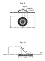
- a two-dimensional image having the colors R, G and B divided by the inclination of the solder surface is generated as shown in Fig. 9.
- a flat surface in a central portion appears as a red image region
- a steep surface in the vicinity of the substrate surface appears as a blue image region
- a comparatively gentle inclined surface appears as a green image region.
- Fig. 10 shows the distribution state of the colors in the case in which the fillet on the substrate is observed by the optical system corresponding to the inclination state of the fillet.
- 50 denotes a substrate surface and S1 denotes a formation range of a land.
- the reflected light which is observed is divided, by the inclination angle of a solder, into blue on an upper steep surface, green on a middle steep surface and red on a surface which is almost flat in the vicinity of the substrate surface.
- a predetermined binary threshold is preset to each of the colors R, G and B.
- the image obtained by the image pick-up device 3 is changed into a binary value by the binary thresholds to extract a binary pattern for each of R, G and B (which will be hereinafter referred to as a "color pattern").
- a pattern obtained in the image of a solder having an excellent shape is previously registered and the feature of each color pattern on the image of an inspection object is compared with that of the registered pattern, thereby deciding the quality of the surface state of the solder.
- the size of a land is reduced with an increase in a density.
- a small-sized substrate such as a substrate for a mobile telephone
- the size of the land is to be reduced.
- the inclination of the fillet is rapidly increased so that it is hard to extract each of the color patterns of R, G and B.
- Fig. 11 shows an example of observation in the case in which the inclination of the fillet is very great.
- a formation range S2 of the land is reduced. Consequently, the fillet is inclined at an angle corresponding to the light source 10 for blue over a whole length so that most of a reflected light which is observed might be blue in some cases.
- an increase in the number of the light sources can be proposed as a method of enhancing a resolution related to the detection of an inclined surface. In this case, a cost is increased.
- a first surface state inspecting method comprises the steps of picking up an image of a light reflected from an inspection object under an illumination condition in which different colored lights are irradiated in a plurality of directions having different elevation angles with respect to the inspection object, selecting and executing a processing of extracting one color component having a maximum intensity in color components corresponding to the colored lights or a processing of extracting the color component having a maximum intensity and a color component having the second highest intensity for each pixel in an image region including an image of the inspection object based on a relationship between the intensities of the color components with respect to the image obtained by the image pick-up, and inspecting a surface state of the inspection object by using image data indicative of a result of the processing of extracting a color component'in the image region.
- the "inspection object” implies a curved surface or a surface having a predetermined inclination angle (including a horizontal surface), for example, a soldered portion on a substrate or a lead of a component.
- the colored lights irradiated in the directions having different elevation angles can have colors of red, green and blue, for example, and are not restricted thereto but two kinds of light sources such as red and green may be used.
- the "image region including an image of the inspection object” can be set to be at least an image region cut out by the contour line of the image of the inspection object (that is, the image of the inspection object itself). Desirably, the same image region is set to be a rectangular region which is larger than the image of the inspection object.
- an image region including a plurality of objects can also be set to be the image region.
- the whole image can be regarded as one image region to be processed.
- the "color component corresponding to each colored light” can be supposed to be the feature amount of a color corresponding to each colored light irradiated in the directions.
- the intensity of each of color signals of red, green and blue can be regarded to be a color component.
- the intensity of each color signal can be expressed by a gradation for each pixel.
- the processing of extracting a color component it is possible to determine to extract only one color component having a maximum intensity or two color components having the color component having a maximum intensity and a color component having the second highest intensity depending on a difference in the intensity between the first color component and the second color component, for example. More specifically, it is preferable that only the first color component should be extracted if the first and second color components make a difference in the intensity which is equal to or greater than a predetermined value, and the first and second color components should be extracted if their difference is smaller than the predetermined value.
- an inclined surface having such an inclination that a mirror reflected light for an irradiated light is incident on an image pick-up device when the light is irradiated from a predetermined light source onto an inspection object will be referred to as "an inclined surface adapted to a light source”.
- two light sources (light sources 8 and 9, and 9 and 10 in Fig. 8) provided without interposing other light sources therebetween will be referred to as "adjacent light sources” and lights emitted from these light sources will be referred to as "lights emitted in directions having adjacent elevation angles”.
- an inclined surface provided in a transition from the inclined surface adapted to one of the adjacent light sources to the inclined surface adapted to the other light source will be referred to as "an inclined surface in a boundary position”.
- the inclined surface of the inspection object is adapted to a predetermined light source
- a color component corresponding to the same light source is supposed to be much more superior to other color components. Therefore, it is possible to obtain an image having the same color as that of the light emitted from the light source by extracting a color component having the highest intensity.
- the intensities of the color components corresponding to the adjacent light sources are close to each other. Consequently, it is possible to obtain an image having a mixed color of the colors corresponding to the adjacent light sources by extracting a color component having a maximum intensity and a color component having the second highest intensity.
- the inclined surfaces adapted in the direction of the arrangement of the light sources 8, 9 and 10 can be expressed by the colors of red, green and blue, respectively. Furthermore, an inclined surface in the boundary position for the light sources 8 and 9 can be expressed by a mixed color of red and green, and an inclined surface between the light sources 9 and 10 can be expressed by a mixed color of green and blue.
- the inclined surface in addition to the colors corresponding to the light sources, thus, it is possible to express the inclined surface by the mixed color of the colors corresponding to the adjacent light sources. Consequently, a resolution related to the detection of an inclination angle can be set more finely based on the distribution state of each color on an image than that in the conventional art.
- the inclination angle of the surface of the inspection object can be recognized with the same resolution as that of the case in which more light sources are provided.
- the step of executing the processing of extracting a color component can include the step of obtaining the mean value of the intensities of the color components and the step of extracting one or two color components which are greater than the mean value in the color components.
- a red component in the image of the inclined surface adapted to the light source 8 for red is overwhelmingly superior to the color components of green and blue. For this reason, only the red component is greater than the mean value of the intensities of the color components.
- the red and green components are greater than the mean value of the color components. Accordingly, it is possible to extract one or two color components depending on the inclination angle of the inclined surface corresponding to a noticed pixel by calculating the mean value of the color components and removing the color component which is less than the mean value for each pixel.
- a pixel having a lower mean value than a predetermined value should be considered to correspond to a portion in which a sufficient reflection cannot be obtained and should be thereby excluded from the object of the extraction processing.
- the step of inspecting a surface state of the inspection object can include the step of grouping each pixel in the region based on a type and combination of an extracted color component in the pixel region after executing the step of the processing of extracting a color component, and the step of deciding a suitability of the surface state of the inspection object based on a distribution state of a pixel belonging to each group.
- a group can be set for each color component and each combination of two color components corresponding to lights emitted in the directions having the adjacent elevation angles.
- a pixel from which only a single color component is extracted is included in the image region of an inclined surface displayed in a color corresponding to the extracted color component.
- a pixel from which two color components are extracted is included in the image region of an inclined surface displayed by a mixed color of the colors corresponding to the extracted color components.
- the surface state of the inspection object can be divided and detected into inclined surfaces corresponding to the number of groups.
- the result obtained by the processing of extracting a color component is varied and the result of the grouping is also changed.
- the distribution state of a pixel belonging to each group can also be varied.
- the distribution state of the pixel belonging to each group can be extracted by a labeling processing for attaching different labels for each group to each pixel, for example. In this case, it is possible to divide and recognize an image region corresponding to each group based on the result of the labeling.
- the number of pixels in each group can also be set to be a parameter indicative of the distribution state of the pixels belonging to the groups.
- the suitability by comparing, with a predetermined reference value, a feature amount (a position of a center of gravity, an area or the like) for each group extracted by the labeling processing or a parameter such as the number of pixels. It is desirable that the feature amount or the parameter for an excellent surface state should be previously calculated by using the image of a model of the inspection object or the like and the reference value should be set based on a value indicative of a result of the calculation.
- the inclined surfaces adapted to the light sources and the inclined surface in their boundary position can be divided and detected based on the distribution state of a pixel belonging to each group. Consequently, the suitability of the surface state of the object can be decided easily with high precision.
- a second surface state inspecting method comprises the steps of picking up an image of a light reflected from an inspection object under an illumination condition in which different colored lights are irradiated in a plurality of directions having different elevation angles with respect to the inspection object, comparing a color component corresponding to a predetermined colored light with a plurality of thresholds set stepwise for each pixel in an image region including an image of the inspection object for the image obtained by the image pick-up, and inspecting a surface state of the inspection object depending on a result of the comparison in the pixel.
- the intensity of the color component corresponding to the same color is changed depending on an inclination angle also in an inclined surface which can be extracted with the color. Accordingly, if a plurality of thresholds are set to the same color component, the angle of the inclined surface can be divided and detected more finely so that a retrieval can be carried out in more detail. Also in the case in which a change in an angle such as the float of a lead is to be detected, moreover, it is possible to detect a very small change in the angle, thereby enhancing precision in the inspection.
- a first substrate inspecting apparatus comprises illuminating means having a plurality of light sources for emitting different colored lights which are provided in directions of different elevation angles with respect to a substrate to be an inspection object respectively, image pick-up means for picking up an image of a light reflected from the substrate, image input means for fetching an image generated by the image pick-up means in a state in which each of the light sources of the illuminating means is turned on, color component extracting means for selecting and executing a processing of extracting one color component having a maximum intensity in color components corresponding to the light sources or a processing of extracting the color component having a maximum intensity and a color component having the second highest intensity based on a relationship of an intensity of each color component for each pixel in an image region including an image of the inspection object with respect to the input image fetched by the image input means, deciding means for deciding a suitability of a surface state of the inspection object by using image data in the image region after executing the processing by the color component extracting means, and output means
- the illuminating means can be provided with a ringshaped light source having different diameters for each color, for example.
- one light source can be constituted by a luminous body group having a plurality of luminous bodies arranged like a ring, for example, an LED.
- a luminous body group having the same color can be arranged concentrically in a plurality of stages, thereby constituting one light source.
- the image pick-up means can be constituted by a CCD camera capable of generating an image signal for each color.
- the image input means is incorporated in a computer for carrying out an image processing for an inspection and serves to generate an image to be a processing object, and can include an amplifying circuit for amplifying an image signal sent from the image pick-up means and an A/D converting circuit for generating a digital image for a processing.
- the image pick-up means is not restricted to a device for generating an analog image signal but may be a digital camera.
- the image input means can be constituted as an input port for individually fetching digital image data for each color.
- the color component extracting means and the deciding means can be constituted by a computer setting a program for performing the step of executing the color component extraction processing and the step of inspecting the surface state of the inspection object, respectively.
- the memory of the computer can store image data obtained after the processing of extracting the image data and color component of a processing object in addition to the program.
- the apparatus having the structure described above, it is possible to more finely detect an inclination angle and automatically decide the suitability of a surface state for a surface such as a solder on a substrate or a lead of a component based on the first method. Consequently, it is possible to carry out an inspection in more detail with the same hardware structure as that in the conventional art and to provide an automatic substrate inspecting apparatus having a high performance without increasing a cost.
- a second substrate inspecting apparatus comprises display means for displaying an image based on each color component extracted by the color component extracting means and input means for accepting the input of data indicative of a result of the decision of the quality for an image displayed by the display means in addition to the same illuminating means, image pick-up means, image input means and color component extracting means as those in the first substrate inspecting apparatus.
- the display means is constituted by a monitor device for displaying an image or display control means for the monitor device.
- the display control means can be constituted by a computer incorporating a program for display control.
- the input means can be constituted by an apparatus for an input operation such as a mouse, a keyboard, a console and the like. Data input by the input means can be output to an external device or the like and can be stored in a predetermined storage medium.
- a third substrate inspecting apparatus comprises the same illuminating means, image pick-up means and image input means as those of the first and second apparatuses, and furthermore, comparing means for comparing a color component corresponding to a predetermined light source with a plurality of thresholds set stepwise for each pixel in an image region including the image of an inspection object with respect to an input image fetched by the image input means, deciding means for deciding the suitability of a surface state of the inspection object by using a result of the comparison in the pixel, and output means for outputting a result of the decision obtained by the deciding means.
- the comparing means and the deciding means should be constituted by a computer setting a program for executing the processings of the respective means.
- the third substrate inspecting apparatus serves to automatically decide the suitability of the surface state of the inspection object.
- the inclination angle of the inclined surface detected as the same color pattern can be decided and detected in detail with a plurality of thresholds. Accordingly, a fillet having a great inclination shown in Fig. 11 and a very small float of a lead can also be detected with high precision so that precision in the decision can be enhanced.
- the same hardware structure as that of the conventional art can be employed. Consequently, it is possible to provide an automatic substrate inspecting apparatus having a high performance without increasing a cost.
- the image input section 12 comprises an amplifying circuit for amplifying each of image signals of R, G and B sent from the image pick-up section 3, an A/D converting circuit for converting the image signals into digital signals, and the like.
- the memory 13 sets an image storage area for storing shaded image data on a digital amount for each of R, G and B, a binary image obtained by changing the shaded images into binary values and the like.
- the input section 19 serves to input various conditions and inspection information for an inspection and is constituted by a keyboard, a mouse and the like.
- the CRT display section 20 (which will be hereinafter referred to as a "display section 20") receives, from the CPU 11, the supply of image data, the result of an inspection and the data input from the input section 19 and displays them on a display screen.
- the printer 21 receives the supply of the result of the inspection and the like from the CPU 11 and prints out the same result in a predetermined format.
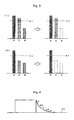
- Fig. 3(2) shows a processing for one pixel in the angle range A1 in Fig. 2.
- the gradation of the red component is higher than two other components, and furthermore, a difference in a gradation between the color components of green and blue is small. Therefore, only the red component has a higher gradation than the mean value Av. In this case, only the gradation of the red component is maintained, while the gradations of the green and blue components are changed to zero.
- Fig. 4 typically shows a color distribution appearing on an image after the execution of the processing of extracting the color component for a fillet on a substrate corresponding to the inclination state of the fillet.
- the inclination angle of the fillet in the illustrated example is changed to be gradually decreased from an angle corresponding to the angle range A3 shown in Fig. 2 and to be flat in a position provided in contact with a substrate surface. Consequently, the color regions of blue (B), a mixed color of blue and green (indicated as BG in the drawing), green (G), a mixed color of green and red (indicated as GR in the drawing) and red (R) sequentially appear in such a direction that the inclination angle is decreased.
- a tone of color is changed depending on the ratio of the intensities of two kinds of color components constituting the mixed color.
- the appearance frequencies of the five kinds of colors on an image can be indicated with the number of pixels belonging to each color group.
- the five kinds of colors indicate the distribution state corresponding to the inclination angle of the soldered surface. If the inclination state of the soldered surface is changed so that the distribution state of each color is varied, therefore, it is a matter of course that the appearance frequency of each color is also changed. More specifically, the number of pixels for each color group can be regarded to be a parameter indicative of the distribution state of the five kinds of colors on the image. For this reason, it is possible to decide the quality of the inclination state of the soldered surface with the number of pixels.
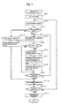
- Fig. 5 shows a procedure during the teaching.
- a step in each processing is indicated as "ST”.
- a decision of "YES" is obtained at a step ST9 and the processing proceeds to a step ST12 in which a decision reference value is set based on the number of pixels obtained finally for each color group. It is desirable that the decision reference value should be smaller corresponding to a predetermined margin than the final number of pixels (for example, a value corresponding to 90% of the final number of pixels and the like).
- a decision of "NO" is obtained at the step ST3.
- data for an inspection using the color patterns of R, G and B are set in the same manner as in the conventional art.
- the person in charge inputs a binary threshold for each of R, G and B by a method of specifying a position having an optimum density on the image of the display section 20.
- the CPU 11 fetches the set value and stores the same set value in the memory 13 corresponding to the set data (position and size) of the inspection region.
- the image of the inspected portion on the substrate is sequentially picked up and the inspection region is set.
- the pixel in the inspection region is classified into the five kinds of color groups to obtain the number of the pixels for each group in the soldered portion and the color patterns of R, G and B are extracted to obtain the feature amounts in portions other than the soldered portion.
- a decision reference value for deciding quality related to the inspection region is set based on the number of the pixels and the feature amount which are thus obtained. Inspection information causing the decision reference value to correspond to the set data in that region (including the binary threshold of each color pattern in a non-soldered portion) is created for the inspection region and is temporarily stored in the memory 13.
- Fig. 6 shows a procedure for an automatic inspection in the substrate inspecting apparatus.
- the steps are indicated by ST21 and subsequent designations.
- the procedure in Fig. 6 is carried out over one substrate and is repeated corresponding to the number of the inspected substrates.
- a decision of "YES" is obtained at a step ST29 and the processing proceeds to a step ST32.
- the number of the pixels obtained for each color group is compared with the decision reference value to decide the quality of the soldered portion.
- a decision of "YES" is obtained at a step ST33.
- steps ST34 to ST36 subsequently, it is decided whether the inspected substrate 1T is an excellent product or a defective product based on the result of the decision for each inspected portion.
- a step ST37 furthermore, the result of the decision is output and the inspection for the inspected substrate 1T is thus ended.
- the distribution state of each color is decided by using the number of the pixels for five kinds of color groups corresponding to five kinds of colors in total including colors corresponding to the light sources 8, 9 and 10 and two kinds of mixed colors corresponding to the adjacent light sources. Therefore, it is possible to finely divide and detect the inclination angle of the soldered surface than that in the conventional art, thereby carrying out a detailed inspection.
- each color component having a maximum intensity or the color component having a maximum intensity and a color component having the second highest intensity is/are extracted from three color components constituting image data for each pixel. Consequently, the inclination state of a solder surface in an image can be expressed by the five kinds of colors.
- the processing of extracting the color component is executed in a visual inspecting apparatus and an image is displayed after the extraction processing. Consequently, it is possible to recognize, in detail, the inclination state of the soldered portion based on the distribution state of the five kinds of colors.
- a plurality of thresholds can be set for the superior color component. According to such setting, it is possible to more finely divide and identify the angle range detected by one color in the conventional art. Referring to the steep surface, therefore, it is also possible to recognize the inclination state in detail, thereby carrying out an inspection with high precision. By reducing the set interval of the threshold, moreover, the resolution of the angle detection can be enhanced. Consequently, it is possible to detect a very small change in an angle with high precision.
- Fig. 7 shows an example of an inspection object in the case in which the state of an IC lead is to be inspected by using a plurality of thresholds set stepwise.
- Fig. 7(1) shows a state in which a float is generated on one lead 31A of a component 30A
- Fig. 7(2) shows a state in which a very small float is generated on a lead 31B in the same position of the same component 30B.
- 32A and 32B denote a lead in a good condition.
Landscapes
- Physics & Mathematics (AREA)
- Health & Medical Sciences (AREA)
- Life Sciences & Earth Sciences (AREA)
- Chemical & Material Sciences (AREA)
- Analytical Chemistry (AREA)
- Biochemistry (AREA)
- General Health & Medical Sciences (AREA)
- General Physics & Mathematics (AREA)
- Immunology (AREA)
- Pathology (AREA)
- Investigating Materials By The Use Of Optical Means Adapted For Particular Applications (AREA)
- Length Measuring Devices By Optical Means (AREA)
- Spectrometry And Color Measurement (AREA)
Abstract
Description
Claims (9)
- A surface state inspecting method comprising the steps of:picking up an image of a light reflected from an inspection object under an illumination condition in which different colored lights are irradiated in a plurality of directions having different elevation angles with respect to the inspection object;selecting and executing a processing of extracting one color component having a maximum intensity in color components corresponding to the colored lights or a processing of extracting the color component having a maximum intensity and a color component having the second highest intensity for each pixel in an image region including an image of the inspection object based on a relationship between the intensities of the color components with respect to the image obtained by the image pick-up; andinspecting a surface state of the inspection object by using image data indicative of a result of the processing of extracting a color component in the image region.
- The surface state inspecting method according to claim 1, wherein the colored lights emitted in the directions have red, green and blue colors and the step of the processing of extracting a color component includes the step of obtaining a mean value of the intensities of the color components and the step of extracting one or two color components which is/are greater than the mean value.
- The surface state inspecting method according to claim 1 or 2, wherein the step of inspecting a surface state of the inspection object includes the step of grouping each pixel in the region based on a type and combination of an extracted color component in the pixel region after executing the step of the processing of extracting a color component, and the step of deciding a suitability of the surface state of the inspection object based on a distribution state of a pixel belonging to each group.
- A surface state inspecting method comprising the steps of:picking up an image of a light reflected from an inspection object under an illumination condition in which different colored lights are irradiated in a plurality of directions having different elevation angles with respect to the inspection object;comparing a color component corresponding to a predetermined colored light with a plurality of thresholds set stepwise for each pixel in an image region including an image of the inspection object for the image obtained by the image pick-up; andinspecting a surface state of the inspection object depending on a result of the comparison in the pixel.
- A substrate inspecting apparatus comprising:illuminating means having a plurality of light sources for emitting different colored lights which are provided in directions of different elevation angles with respect to a substrate to be an inspection object, respectively;image pick-up means for picking up an image of a light reflected from the substrate;image input means for fetching an image generated by the image pick-up means in a state in which each of the light sources of the illuminating means is turned on;color component extracting means for selecting and executing a processing of extracting one color component having a maximum intensity in color components corresponding to the light sources or a processing of extracting the color component having a maximum intensity and a color component having the second highest intensity based on a relationship of an intensity of each color component for each pixel in an image region including an image of the inspection object with respect to the input image fetched by the image input means;deciding means for deciding a suitability of a surface state of the inspection object by using image data in the image region after executing the processing by the color component extracting means; andoutput means for outputting a result of the decision carried out by the deciding means.
- The substrate inspecting apparatus according to claim 5, wherein the illuminating means includes three kinds of light sources for emitting colored lights of red, green and blue, and
the color component extracting means includes means for calculating a mean value of the intensities of the color components corresponding to each of the light sources and means for extracting one or two color components which is/are greater than the mean value thus calculated. - The substrate inspecting apparatus according to claim 5 or 6, wherein the deciding means includes means for grouping each pixel in the image region based on a type and combination of the extracted color component after the processing of the color component extracting means, thereby deciding a suitability of a surface state of the inspection object based on a distribution state of a pixel belonging to each group.
- A substrate inspecting apparatus comprising:illuminating means having a plurality of light sources for emitting different colored lights which are provided in directions of different elevation angles with respect to a substrate to be an inspection object, respectively;image pick-up means for picking up an image of a light reflected from the substrate;image input means for fetching an image generated by the image pick-up means in a state in which each of the light sources of the illuminating means is turned on;color component extracting means for selecting and executing a processing of extracting one color component having a maximum intensity in color components corresponding to the light sources or a processing of extracting the color component having a maximum intensity and a color component having the second highest intensity based on a relationship of an intensity of each color component for each pixel in an image region including an image of the inspection object with respect to the input image fetched by the image input means;display means for displaying an image by each color component extracted by the color component extracting means; andinput means for accepting an input of data indicative of a result of a decision of quality for the image displayed by the display means.
- A substrate inspecting apparatus comprising:illuminating means having a plurality of light sources for emitting different colored lights which are provided in directions of different elevation angles with respect to a substrate of an inspection object, respectively;image pick-up means for picking up an image of a light reflected from the substrate;image input means for fetching an image generated by the image pick-up means in a state in which each of the light sources of the illuminating means is turned on;comparing means for comparing a color component corresponding to a predetermined light source with a plurality of thresholds set stepwise for each pixel in an image region including an image of the inspection object with respect to the input image fetched by the image input means;deciding means for deciding a suitability of a surface state of the inspection object by using a result of the comparison in the pixel; and output means for outputting a result of the decision carried out by the deciding means.
Applications Claiming Priority (4)
| Application Number | Priority Date | Filing Date | Title |
|---|---|---|---|
| JP2002003449 | 2002-01-10 | ||
| JP2002003449 | 2002-01-10 | ||
| JP2002364400 | 2002-12-16 | ||
| JP2002364400A JP3551188B2 (en) | 2002-01-10 | 2002-12-16 | Surface condition inspection method and substrate inspection device |
Publications (3)
| Publication Number | Publication Date |
|---|---|
| EP1333275A2 true EP1333275A2 (en) | 2003-08-06 |
| EP1333275A3 EP1333275A3 (en) | 2004-04-07 |
| EP1333275B1 EP1333275B1 (en) | 2008-08-27 |
Family
ID=26625476
Family Applications (1)
| Application Number | Title | Priority Date | Filing Date |
|---|---|---|---|
| EP02028989A Expired - Lifetime EP1333275B1 (en) | 2002-01-10 | 2002-12-27 | Method and apparatus for inspecting the surface of substrates |
Country Status (6)
| Country | Link |
|---|---|
| US (1) | US6947151B2 (en) |
| EP (1) | EP1333275B1 (en) |
| JP (1) | JP3551188B2 (en) |
| CN (1) | CN1195978C (en) |
| DE (1) | DE60228542D1 (en) |
| TW (1) | TW583389B (en) |
Cited By (5)
| Publication number | Priority date | Publication date | Assignee | Title |
|---|---|---|---|---|
| WO2004038394A1 (en) * | 2002-10-25 | 2004-05-06 | Siemens Aktiengesellschaft | Method for the quality control of connection balls of electronic components |
| FR2920227A1 (en) * | 2007-08-24 | 2009-02-27 | Vit Sa | Electronic board inspecting method, involves subdividing reflected images into analysis zone, allocating reflected ray values to analysis zone, realizing signature of zone, and comparing signature of zone to reference signature |
| EP1568985A3 (en) * | 2004-02-27 | 2010-12-29 | Omron Corporation | Apparatus for surface inspection and method and apparatus for inspecting substrate |
| CN108827971A (en) * | 2018-04-26 | 2018-11-16 | 深圳市创科自动化控制技术有限公司 | A kind of detection method of surface flaw |
| EP3767938A4 (en) * | 2018-03-14 | 2021-03-03 | Fuji Corporation | IMAGE CAPTURE UNIT AND COMPONENT MOUNTING DEVICE |
Families Citing this family (63)
| Publication number | Priority date | Publication date | Assignee | Title |
|---|---|---|---|---|
| US7062080B2 (en) * | 2001-11-26 | 2006-06-13 | Omron Corporation | Method of inspecting curved surface and device for inspecting printed circuit board |
| US9092841B2 (en) | 2004-06-09 | 2015-07-28 | Cognex Technology And Investment Llc | Method and apparatus for visual detection and inspection of objects |
| TWI221531B (en) * | 2002-10-25 | 2004-10-01 | Hwan-Chia Chang | Method for testing soldering reliability |
| US7356176B2 (en) * | 2004-02-26 | 2008-04-08 | Omron Corporation | Mounting-error inspecting method and substrate inspecting apparatus using the method |
| US8891852B2 (en) | 2004-06-09 | 2014-11-18 | Cognex Technology And Investment Corporation | Method and apparatus for configuring and testing a machine vision detector |
| US8127247B2 (en) | 2004-06-09 | 2012-02-28 | Cognex Corporation | Human-machine-interface and method for manipulating data in a machine vision system |
| US9292187B2 (en) | 2004-11-12 | 2016-03-22 | Cognex Corporation | System, method and graphical user interface for displaying and controlling vision system operating parameters |
| JP4736764B2 (en) * | 2005-01-11 | 2011-07-27 | オムロン株式会社 | Substrate inspection device, inspection logic setting method and inspection logic setting device |
| US7769226B2 (en) | 2005-01-26 | 2010-08-03 | Semiconductor Energy Laboratory Co., Ltd. | Pattern inspection method and apparatus |
| US7315361B2 (en) * | 2005-04-29 | 2008-01-01 | Gsi Group Corporation | System and method for inspecting wafers in a laser marking system |
| JP2006318214A (en) * | 2005-05-12 | 2006-11-24 | Omron Corp | Feature acquisition device and conversion device |
| US7391510B2 (en) * | 2006-01-26 | 2008-06-24 | Orbotech Ltd | System and method for inspecting patterned devices having microscopic conductors |
| JP4801457B2 (en) * | 2006-02-02 | 2011-10-26 | 株式会社リコー | Surface defect inspection apparatus, surface defect inspection method, and surface defect inspection program |
| CN101150732B (en) * | 2006-09-20 | 2010-08-11 | 王锦峰 | Imaging method and device for taking color images with black and white camera |
| JP4389982B2 (en) * | 2007-08-09 | 2009-12-24 | オムロン株式会社 | Substrate visual inspection device |
| US8103085B1 (en) * | 2007-09-25 | 2012-01-24 | Cognex Corporation | System and method for detecting flaws in objects using machine vision |
| DE102007049702A1 (en) * | 2007-10-17 | 2009-04-23 | Robert Bosch Gmbh | picking line |
| JP4611404B2 (en) * | 2008-06-04 | 2011-01-12 | 本田技研工業株式会社 | Belt inspection device |
| DE102008057131B4 (en) | 2007-12-06 | 2013-05-29 | Honda Motor Co., Ltd. | Riemenprüfvorrichtung |
| JP4503643B2 (en) * | 2007-12-06 | 2010-07-14 | 本田技研工業株式会社 | Metal belt inspection device |
| DE102008013525B4 (en) * | 2008-03-08 | 2010-07-29 | Nordischer Maschinenbau Rud. Baader Gmbh + Co Kg | Apparatus and method for contactless identification of characteristics of continuously conveyed, translucent products |
| US8077307B2 (en) * | 2008-04-09 | 2011-12-13 | Orbotech Ltd. | Illumination system for optical inspection |
| KR100902170B1 (en) * | 2008-05-19 | 2009-06-10 | (주)펨트론 | Surface shape measuring device |
| TW200949241A (en) * | 2008-05-28 | 2009-12-01 | Asustek Comp Inc | Apparatus and method for detecting circuit board |
| JP4719284B2 (en) | 2008-10-10 | 2011-07-06 | トヨタ自動車株式会社 | Surface inspection device |
| KR100955272B1 (en) | 2009-01-29 | 2010-04-30 | (주)펨트론 | Surface shape measuring device |
| JP5108827B2 (en) * | 2009-04-28 | 2012-12-26 | ヴィスコ・テクノロジーズ株式会社 | Shape inspection apparatus and shape inspection program |
| JP5065329B2 (en) * | 2009-05-12 | 2012-10-31 | ヴィスコ・テクノロジーズ株式会社 | Shape inspection apparatus and shape inspection program |
| IT1395116B1 (en) * | 2009-07-29 | 2012-09-05 | Utpvision S R L | OPTICAL SURFACE DETECTION SYSTEM |
| JP5471306B2 (en) * | 2009-10-28 | 2014-04-16 | ソニー株式会社 | Color unevenness inspection apparatus and color unevenness inspection method |
| JP2012063269A (en) * | 2010-09-16 | 2012-03-29 | Sony Corp | Measuring apparatus and measuring method |
| CN102364332B (en) * | 2011-06-10 | 2014-07-30 | 乐金化学(南京)信息电子材料有限公司 | Polarizing plate movement detection apparatus and method thereof |
| KR101248143B1 (en) * | 2011-06-24 | 2013-03-28 | 주식회사 에스에프이 | Image processing module and led chip bonding apparatus using thereof |
| JP6032696B2 (en) * | 2011-06-30 | 2016-11-30 | 芝浦メカトロニクス株式会社 | Bonded plate inspection apparatus and method |
| US9651499B2 (en) | 2011-12-20 | 2017-05-16 | Cognex Corporation | Configurable image trigger for a vision system and method for using the same |
| TWI597472B (en) * | 2012-02-03 | 2017-09-01 | Aist | Method and device for measuring the height of protrusions and even protrusions on the surface of articles |
| KR101438157B1 (en) * | 2012-11-12 | 2014-09-05 | 주식회사 고영테크놀러지 | Board inspection method |
| KR101590831B1 (en) * | 2013-04-02 | 2016-02-03 | 주식회사 고영테크놀러지 | Method of inspecting foreign substance on a board |
| WO2014188457A1 (en) * | 2013-05-23 | 2014-11-27 | Centro Sviluppo Materiali S.P.A. | Method for the surface inspection of long products and apparatus suitable for carrying out such a method |
| EP3070431B1 (en) * | 2014-01-08 | 2023-12-06 | Yamaha Hatsudoki Kabushiki Kaisha | Visual inspection device and visual inspection method |
| TWI495867B (en) * | 2014-07-22 | 2015-08-11 | Machvision Inc | Application of repeated exposure to multiple exposure image blending detection method |
| CN105987916A (en) * | 2015-01-29 | 2016-10-05 | 三垦电气株式会社 | Image detection device and image detection method |
| WO2016142986A1 (en) * | 2015-03-06 | 2016-09-15 | 富士機械製造株式会社 | Recognition device and recognition method |
| CN104764752B (en) * | 2015-03-24 | 2017-09-12 | 广州视源电子科技股份有限公司 | Solder joint tin connection detection method and device |
| CN106153625A (en) * | 2015-04-01 | 2016-11-23 | 五邑大学 | Surface scratch detection method based on colourama reflection differences |
| JP2017067633A (en) * | 2015-09-30 | 2017-04-06 | キヤノン株式会社 | Checkup apparatus, and manufacturing method |
| JP6791631B2 (en) * | 2016-01-06 | 2020-11-25 | 株式会社サキコーポレーション | Image generation method and inspection equipment |
| CN106289099B (en) * | 2016-07-28 | 2018-11-20 | 汕头大学 | A kind of single camera vision system and the three-dimensional dimension method for fast measuring based on the system |
| CN106645161B (en) * | 2016-09-27 | 2020-02-04 | 凌云光技术集团有限责任公司 | Surface defect detection system and method |
| JP6673268B2 (en) * | 2017-03-14 | 2020-03-25 | オムロン株式会社 | Management device, control method of management device, information processing program, and recording medium |
| EP3723357B1 (en) * | 2017-12-05 | 2025-11-26 | Fuji Corporation | Imaging unit and component mounting machine |
| JP6969439B2 (en) * | 2018-02-23 | 2021-11-24 | オムロン株式会社 | Visual inspection device and lighting condition setting method for visual inspection device |
| JP7125880B2 (en) * | 2018-09-27 | 2022-08-25 | オルガノ株式会社 | Inspection device and inspection method |
| JP7189351B2 (en) * | 2019-07-26 | 2022-12-13 | 株式会社Fuji | lighting unit |
| US11282187B2 (en) * | 2019-08-19 | 2022-03-22 | Ricoh Company, Ltd. | Inspection system, inspection apparatus, and method using multiple angle illumination |
| US11189372B2 (en) * | 2019-09-19 | 2021-11-30 | Rx-V Inc. | Verification system for medication packaging and method |
| JP2021089159A (en) | 2019-12-02 | 2021-06-10 | Juki株式会社 | Inspection device and inspection method |
| WO2022113369A1 (en) * | 2020-11-30 | 2022-06-02 | ヤマハ発動機株式会社 | Mounting-board inspection apparatus and inspection apparatus |
| CN113029102A (en) * | 2021-04-26 | 2021-06-25 | 四川大学 | Inclination angle measuring device for house safety monitoring |
| CN113298793B (en) * | 2021-06-03 | 2023-11-24 | 中国电子科技集团公司第十四研究所 | A method for circuit board surface defect detection based on multi-view template matching |
| JP7822791B2 (en) * | 2022-01-12 | 2026-03-03 | 東京エレクトロン株式会社 | Substrate inspection device, substrate inspection method, and substrate inspection program |
| CN115436381B (en) * | 2022-09-09 | 2025-11-28 | 新恒汇电子股份有限公司 | Full-automatic lead frame film pasting visual defect detection system and detection method |
| CN116148265B (en) * | 2023-02-14 | 2024-07-12 | 浙江迈沐智能科技有限公司 | Flaw analysis method and system based on synthetic leather high-quality image acquisition |
Family Cites Families (11)
| Publication number | Priority date | Publication date | Assignee | Title |
|---|---|---|---|---|
| JPS61293657A (en) * | 1985-06-21 | 1986-12-24 | Matsushita Electric Works Ltd | Method for inspecting soldering appearance |
| JPS62127617A (en) * | 1985-11-29 | 1987-06-09 | Fujitsu Ltd | Inspecting instrument for linear body |
| JPH061173B2 (en) | 1988-05-09 | 1994-01-05 | オムロン株式会社 | Curved property inspection device |
| ATE135110T1 (en) * | 1988-05-09 | 1996-03-15 | Omron Tateisi Electronics Co | SUBSTRATE TESTING DEVICE |
| US5039868A (en) * | 1988-11-24 | 1991-08-13 | Omron Corporation | Method of and apparatus for inspecting printed circuit boards and the like |
| JPH02231510A (en) * | 1989-03-02 | 1990-09-13 | Omron Tateisi Electron Co | Substrate inspection device |
| US5064291A (en) * | 1990-04-03 | 1991-11-12 | Hughes Aircraft Company | Method and apparatus for inspection of solder joints utilizing shape determination from shading |
| JP3072998B2 (en) * | 1990-04-18 | 2000-08-07 | 株式会社日立製作所 | Soldering condition inspection method and apparatus |
| EP0526080B1 (en) * | 1991-07-22 | 1996-10-02 | Omron Corporation | Teaching method and system for mounted component inspection |
| KR100200215B1 (en) * | 1996-04-08 | 1999-06-15 | 윤종용 | Soldering detection apparatus & method thereof using corelated neural network |
| US6040895A (en) * | 1997-10-08 | 2000-03-21 | Siemens Aktiengesellschaft | Method and device for controlled illumination of an object for improving identification of an object feature in an image of the object |
-
2002
- 2002-12-16 JP JP2002364400A patent/JP3551188B2/en not_active Expired - Fee Related
- 2002-12-27 DE DE60228542T patent/DE60228542D1/en not_active Expired - Lifetime
- 2002-12-27 EP EP02028989A patent/EP1333275B1/en not_active Expired - Lifetime
-
2003
- 2003-01-08 TW TW092100289A patent/TW583389B/en not_active IP Right Cessation
- 2003-01-08 US US10/338,020 patent/US6947151B2/en not_active Expired - Fee Related
- 2003-01-09 CN CNB031034675A patent/CN1195978C/en not_active Expired - Fee Related
Cited By (6)
| Publication number | Priority date | Publication date | Assignee | Title |
|---|---|---|---|---|
| WO2004038394A1 (en) * | 2002-10-25 | 2004-05-06 | Siemens Aktiengesellschaft | Method for the quality control of connection balls of electronic components |
| EP1568985A3 (en) * | 2004-02-27 | 2010-12-29 | Omron Corporation | Apparatus for surface inspection and method and apparatus for inspecting substrate |
| FR2920227A1 (en) * | 2007-08-24 | 2009-02-27 | Vit Sa | Electronic board inspecting method, involves subdividing reflected images into analysis zone, allocating reflected ray values to analysis zone, realizing signature of zone, and comparing signature of zone to reference signature |
| WO2009050349A3 (en) * | 2007-08-24 | 2009-07-30 | Vit | Method for inspecting electronic boards using multispectral analysis |
| EP3767938A4 (en) * | 2018-03-14 | 2021-03-03 | Fuji Corporation | IMAGE CAPTURE UNIT AND COMPONENT MOUNTING DEVICE |
| CN108827971A (en) * | 2018-04-26 | 2018-11-16 | 深圳市创科自动化控制技术有限公司 | A kind of detection method of surface flaw |
Also Published As
| Publication number | Publication date |
|---|---|
| US6947151B2 (en) | 2005-09-20 |
| TW200301817A (en) | 2003-07-16 |
| JP2003270173A (en) | 2003-09-25 |
| TW583389B (en) | 2004-04-11 |
| JP3551188B2 (en) | 2004-08-04 |
| CN1195978C (en) | 2005-04-06 |
| EP1333275A3 (en) | 2004-04-07 |
| DE60228542D1 (en) | 2008-10-09 |
| EP1333275B1 (en) | 2008-08-27 |
| CN1431482A (en) | 2003-07-23 |
| US20030169418A1 (en) | 2003-09-11 |
Similar Documents
| Publication | Publication Date | Title |
|---|---|---|
| EP1333275B1 (en) | Method and apparatus for inspecting the surface of substrates | |
| US7505149B2 (en) | Apparatus for surface inspection and method and apparatus for inspecting substrate | |
| US7822261B2 (en) | Board inspecting apparatus, its parameter setting method and parameter setting apparatus | |
| JP3594026B2 (en) | Surface condition inspection method and substrate inspection device for curved body | |
| JP4506395B2 (en) | Substrate inspection device, parameter setting method and parameter setting device | |
| JP2000131037A (en) | Object shape inspection device | |
| JP4539355B2 (en) | Substrate inspection device, parameter setting method and parameter setting device | |
| JP3599023B2 (en) | Solder inspection method and board inspection apparatus using this method | |
| JP2006194607A (en) | Substrate inspection device, parameter setting method and parameter setting device | |
| JP3622749B2 (en) | Curved surface property inspection method and substrate inspection apparatus using this method | |
| CN100582755C (en) | Substrate inspection device, method for setting inspection logic, and device for setting inspection logic | |
| JP2007033126A (en) | Substrate inspection apparatus, parameter adjustment method thereof, and parameter adjustment apparatus | |
| CN1979137A (en) | Substrate inspection device, method and device for setting inspection logic | |
| JP4453503B2 (en) | Substrate inspection device, substrate inspection method, inspection logic generation device and inspection logic generation method for substrate inspection device | |
| JP2002250700A (en) | Pattern inspection method and apparatus | |
| JP4507785B2 (en) | Substrate inspection device, parameter setting method and parameter setting device | |
| JP4858227B2 (en) | Inspection parameter setting support device, control program and control method thereof | |
| JP2006322951A (en) | Surface condition inspection method, surface condition inspection apparatus and substrate inspection apparatus using the method | |
| US6088109A (en) | System for detecting the presence of deposited metals on soldering points of an integrated circuit board substrate | |
| JP2006078285A (en) | Substrate inspection device, parameter setting method and parameter setting device | |
| JP4419778B2 (en) | Substrate inspection device, parameter setting method and parameter setting device | |
| JP2000329532A (en) | Pattern defect extraction method and parameter determination method used therefor | |
| JPH07120231A (en) | Appearance inspection device | |
| JPH0627030A (en) | Soldering inspection device |
Legal Events
| Date | Code | Title | Description |
|---|---|---|---|
| PUAI | Public reference made under article 153(3) epc to a published international application that has entered the european phase |
Free format text: ORIGINAL CODE: 0009012 |
|
| AK | Designated contracting states |
Designated state(s): AT BE BG CH CY CZ DE DK EE ES FI FR GB GR IE IT LI LU MC NL PT SE SI SK TR |
|
| AX | Request for extension of the european patent |
Extension state: AL LT LV MK RO |
|
| RIN1 | Information on inventor provided before grant (corrected) |
Inventor name: MURAKAMI, KIYOSHI,C/O OMRON CORP.,801, MINAMIFUD Inventor name: FUJII, YOSHIKI,C/O OMRON CORP.801, MINAMIFUDODO- |
|
| PUAL | Search report despatched |
Free format text: ORIGINAL CODE: 0009013 |
|
| AK | Designated contracting states |
Kind code of ref document: A3 Designated state(s): AT BE BG CH CY CZ DE DK EE ES FI FR GB GR IE IT LI LU MC NL PT SE SI SK TR |
|
| AX | Request for extension of the european patent |
Extension state: AL LT LV MK RO |
|
| 17P | Request for examination filed |
Effective date: 20040629 |
|
| AKX | Designation fees paid |
Designated state(s): DE GB IT |
|
| 17Q | First examination report despatched |
Effective date: 20050208 |
|
| GRAP | Despatch of communication of intention to grant a patent |
Free format text: ORIGINAL CODE: EPIDOSNIGR1 |
|
| RIC1 | Information provided on ipc code assigned before grant |
Ipc: G01N 21/88 20060101AFI20070921BHEP Ipc: G01N 21/956 20060101ALI20070921BHEP |
|
| RAP1 | Party data changed (applicant data changed or rights of an application transferred) |
Owner name: OMRON CORPORATION, A CORPORATION OF JAPAN |
|
| GRAS | Grant fee paid |
Free format text: ORIGINAL CODE: EPIDOSNIGR3 |
|
| RIN1 | Information on inventor provided before grant (corrected) |
Inventor name: FUJII, YOSHIKI,C Inventor name: MURAKAMI, KIYOSHI,C |
|
| RIN1 | Information on inventor provided before grant (corrected) |
Inventor name: MURAKAMI, KIYOSHI,C Inventor name: FUJII, YOSHIKI,C |
|
| GRAA | (expected) grant |
Free format text: ORIGINAL CODE: 0009210 |
|
| AK | Designated contracting states |
Kind code of ref document: B1 Designated state(s): DE GB IT |
|
| REG | Reference to a national code |
Ref country code: GB Ref legal event code: FG4D |
|
| REF | Corresponds to: |
Ref document number: 60228542 Country of ref document: DE Date of ref document: 20081009 Kind code of ref document: P |
|
| PLBE | No opposition filed within time limit |
Free format text: ORIGINAL CODE: 0009261 |
|
| STAA | Information on the status of an ep patent application or granted ep patent |
Free format text: STATUS: NO OPPOSITION FILED WITHIN TIME LIMIT |
|
| 26N | No opposition filed |
Effective date: 20090528 |
|
| REG | Reference to a national code |
Ref country code: DE Ref legal event code: R082 Ref document number: 60228542 Country of ref document: DE Representative=s name: KILIAN KILIAN & PARTNER, DE |
|
| PGFP | Annual fee paid to national office [announced via postgrant information from national office to epo] |
Ref country code: GB Payment date: 20121214 Year of fee payment: 11 Ref country code: IT Payment date: 20121213 Year of fee payment: 11 |
|
| PGFP | Annual fee paid to national office [announced via postgrant information from national office to epo] |
Ref country code: DE Payment date: 20121227 Year of fee payment: 11 |
|
| REG | Reference to a national code |
Ref country code: DE Ref legal event code: R119 Ref document number: 60228542 Country of ref document: DE |
|
| GBPC | Gb: european patent ceased through non-payment of renewal fee |
Effective date: 20131227 |
|
| REG | Reference to a national code |
Ref country code: DE Ref legal event code: R119 Ref document number: 60228542 Country of ref document: DE Effective date: 20140701 |
|
| PG25 | Lapsed in a contracting state [announced via postgrant information from national office to epo] |
Ref country code: DE Free format text: LAPSE BECAUSE OF NON-PAYMENT OF DUE FEES Effective date: 20140701 |
|
| PG25 | Lapsed in a contracting state [announced via postgrant information from national office to epo] |
Ref country code: GB Free format text: LAPSE BECAUSE OF NON-PAYMENT OF DUE FEES Effective date: 20131227 |
|
| PG25 | Lapsed in a contracting state [announced via postgrant information from national office to epo] |
Ref country code: IT Free format text: LAPSE BECAUSE OF NON-PAYMENT OF DUE FEES Effective date: 20131231 |
|
| PG25 | Lapsed in a contracting state [announced via postgrant information from national office to epo] |
Ref country code: IT Free format text: LAPSE BECAUSE OF NON-PAYMENT OF DUE FEES Effective date: 20131227 |