EP1333258A1 - Method for correcting sensor output - Google Patents
Method for correcting sensor output Download PDFInfo
- Publication number
- EP1333258A1 EP1333258A1 EP01982755A EP01982755A EP1333258A1 EP 1333258 A1 EP1333258 A1 EP 1333258A1 EP 01982755 A EP01982755 A EP 01982755A EP 01982755 A EP01982755 A EP 01982755A EP 1333258 A1 EP1333258 A1 EP 1333258A1
- Authority
- EP
- European Patent Office
- Prior art keywords
- light
- sensor
- output
- linearizing
- sensor output
- Prior art date
- Legal status (The legal status is an assumption and is not a legal conclusion. Google has not performed a legal analysis and makes no representation as to the accuracy of the status listed.)
- Granted
Links
Images















Classifications
-
- G—PHYSICS
- G01—MEASURING; TESTING
- G01J—MEASUREMENT OF INTENSITY, VELOCITY, SPECTRAL CONTENT, POLARISATION, PHASE OR PULSE CHARACTERISTICS OF INFRARED, VISIBLE OR ULTRAVIOLET LIGHT; COLORIMETRY; RADIATION PYROMETRY
- G01J1/00—Photometry, e.g. photographic exposure meter
- G01J1/10—Photometry, e.g. photographic exposure meter by comparison with reference light or electric value provisionally void
- G01J1/16—Photometry, e.g. photographic exposure meter by comparison with reference light or electric value provisionally void using electric radiation detectors
- G01J1/1626—Arrangements with two photodetectors, the signals of which are compared
-
- G—PHYSICS
- G01—MEASURING; TESTING
- G01J—MEASUREMENT OF INTENSITY, VELOCITY, SPECTRAL CONTENT, POLARISATION, PHASE OR PULSE CHARACTERISTICS OF INFRARED, VISIBLE OR ULTRAVIOLET LIGHT; COLORIMETRY; RADIATION PYROMETRY
- G01J1/00—Photometry, e.g. photographic exposure meter
- G01J1/10—Photometry, e.g. photographic exposure meter by comparison with reference light or electric value provisionally void
- G01J1/12—Photometry, e.g. photographic exposure meter by comparison with reference light or electric value provisionally void using wholly visual means
- G01J1/122—Visual exposure meters for determining the exposure time in photographical recording or reproducing
- G01J1/124—Visual exposure meters for determining the exposure time in photographical recording or reproducing based on the comparison of the intensity of measured light with a comparison source or comparison illuminated surface
-
- G—PHYSICS
- G01—MEASURING; TESTING
- G01N—INVESTIGATING OR ANALYSING MATERIALS BY DETERMINING THEIR CHEMICAL OR PHYSICAL PROPERTIES
- G01N21/00—Investigating or analysing materials by the use of optical means, i.e. using sub-millimetre waves, infrared, visible or ultraviolet light
- G01N21/17—Systems in which incident light is modified in accordance with the properties of the material investigated
- G01N21/47—Scattering, i.e. diffuse reflection
- G01N21/4738—Diffuse reflection, e.g. also for testing fluids, fibrous materials
-
- G—PHYSICS
- G01—MEASURING; TESTING
- G01N—INVESTIGATING OR ANALYSING MATERIALS BY DETERMINING THEIR CHEMICAL OR PHYSICAL PROPERTIES
- G01N21/00—Investigating or analysing materials by the use of optical means, i.e. using sub-millimetre waves, infrared, visible or ultraviolet light
- G01N21/17—Systems in which incident light is modified in accordance with the properties of the material investigated
- G01N21/59—Transmissivity
-
- G—PHYSICS
- G01—MEASURING; TESTING
- G01N—INVESTIGATING OR ANALYSING MATERIALS BY DETERMINING THEIR CHEMICAL OR PHYSICAL PROPERTIES
- G01N21/00—Investigating or analysing materials by the use of optical means, i.e. using sub-millimetre waves, infrared, visible or ultraviolet light
- G01N21/17—Systems in which incident light is modified in accordance with the properties of the material investigated
- G01N21/59—Transmissivity
- G01N21/5907—Densitometers
- G01N2021/5915—Processing scan data in densitometry
- G01N2021/5949—Correcting nonlinearity of signal, e.g. in measurement of photomedium
-
- G—PHYSICS
- G01—MEASURING; TESTING
- G01N—INVESTIGATING OR ANALYSING MATERIALS BY DETERMINING THEIR CHEMICAL OR PHYSICAL PROPERTIES
- G01N21/00—Investigating or analysing materials by the use of optical means, i.e. using sub-millimetre waves, infrared, visible or ultraviolet light
- G01N21/17—Systems in which incident light is modified in accordance with the properties of the material investigated
- G01N21/59—Transmissivity
- G01N21/5907—Densitometers
- G01N2021/5957—Densitometers using an image detector type detector, e.g. CCD
Definitions
- the present invention relates to a method in which light is applied to a measuring object and measurements are carried out by receiving light reflected from a detection subject portion by a sensor, and, more specifically, concerns a correction method for a sensor output when the sensor used in this method does not have output linearity with respect to the quantity of received light.
- the light to be measured includes various kinds of light, such as reflected light, transmitted light, fluorescent light, phosphor light and chemically emitted light, which are used in quantitative measurements and qualitative measurements.
- Photodetectors include a photodetector element constituted by a single element such as a photodiode, a linear sensor constituted by photodetector elements that are aligned on a line, such as a photodiode array, and an area sensor constituted by photodetector elements that are arranged two-dimensionally, such as a CCD sensor and a CMOS sensor.
- sensor output characteristics relating to quantity of received light there are not only sensors having linearity such as photodiodes, but also sensors having sensing characteristics that have deviations in linearity depending on areas having a small quantity of received light and those having a great quantity of received light, as in the case of area sensors such as CCD sensors and MOS sensors. Those sensors that lack linearity have been considered to be unsuitable for quantitative measurements.
- the objective of the present invention is to solve problems with linearity that occur when a sensor that lacks linearity in its output characteristics is used in a detector, and consequently to make such a sensor applicable to corresponding measurements.
- the present invention relates to a method which applies light to a measuring object and carries out measurements by receiving light reflected from a detection subject portion by a sensor, and in such a method, with respect to the sensor, such a sensor that lacks linearity in its output in response to the quantity of received light is used. Further, the present invention is characterized by a linearizing process that corrects the sensor output so that the output from the sensor in response to a variation in the quantity of received light in the sensor is made proportional to the quantity of received light.
- the linearizing process includes the following processes (A) and (B):
- the sensor output does not have linearity with respect to the quantity of received light, it is corrected so as to be made proportional to the output of the photodetector whose output has linearity with respect to the quantity of received light based upon the linearizing data; thus, the corrected sensor output is allowed to have linearity with respect to the quantity of received light.
- the linearizing process includes the following processes (A) and (B):
- the sensor output does not have linearity with respect to the quantity of received light, it is corrected so as to be made proportional to light from the standard plate based upon the linearizing data; thus, the corrected sensor output is allowed to have linearity with respect to the quantity of received light.
- the second aspect it is not necessary to separately install a light-quantity-monitoring photodetector whose output has linearity with respect to the quantity of received light and a measuring device for the photodetector.
- the standard plate is exchanged and a measurement is simply carried out so that the operation is easily carried out.
- the correction is made by using data derived from light actually received by the sensor, it is possible to reduce error factors.
- the linearizing process includes the following processes (A) and (B):
- a reflection plate having even in-plane density or a blank state (a state in which all the measuring light is made incident on an image sensor without placing a measuring object) is prepared.
- the quantity of received light of the sensor is proportional to exposing time during which the reference object is exposed.
- the sensor output does not have linearity with respect to the quantity of received light, it is corrected so as to be made proportional to light from the reference object which is found from the exposing time, based upon the linearizing data; thus, the corrected sensor output is allowed to have linearity with respect to the quantity of received light.
- linearizing data can be formed by using only one sheet of reference object that forms the standard; therefore, it is possible to make the operation easier.
- An example of a sensor suitable for use in accordance with the present invention is an area sensor.
- the above-mentioned linearizing process is carried out on each pixel.
- the linearizing process may be carried out by selecting some of pixels in the vicinity of pixels that are brightest within an image and using the average value of the outputs of these pixels.
- Examples of the area sensor include those of the CCD type or CMOS type.
- the output of the sensor is preferably prepared as a value that has been subjected to an offset process, that is, a value obtained by subtracting an output at the time when the quantity of received light is zero as dark data.
- An example of an analyzer to which the sensor is applied is a reflectance measuring device.
- a photodiode has been mainly used from the viewpoint of superior precision, cost performance and technical easiness.
- an optical system or a test sample needs to be shifted.
- the photodiode is used for obtaining data that is averaged within a spot diameter, it is not suitable for use in precisely detecting color developments, as typically exemplified by detection of spot color developments.
- data of the area sensor is image information relating to a target area
- measurements of a plurality of items, detection of spot color developments, correction of positional deviations in test samples, etc. may be carried out based upon information of one frame.
- Detections of the shape and color of a subject by the use of an area sensor have been well-known.
- a method in which an image of a test strip for use in immunization measurements is picked up by a CCD camera so that determination is made based upon the area or the ratio of the longitudinal and lateral lengths of the image has been proposed (see Japanese Patent Application Laid-Open No. 9-257708).
- the picked-up signal has been binarized as a luminance signal
- the shape of an image is measured; therefore, this method is not used for measuring the density within the image.
- a urine measuring device is listed.
- measurements are carried out by determining not the density (brightness) in color developments, but the color gradation (hue) in urine test paper, and a color-CCD device is used.
- a light-irregularity correction process which, after a reference object has been measured as a measuring object, corrects the outputs of the respective pixels so that corrected values, obtained by subjecting the corresponding outputs of the respective pixels of the area sensor to the above-mentioned linearizing process, are evenly adjusted.
- the raw image information, picked up by the measuring device using the area sensor, is subjected to influences from individual differences in sensitivity of the respective pixels, irradiation irregularities of a light source (for example, LED), cosine quadruple rule (aberration) of the lens and the like.
- the "light irregularities" are caused by all these influences.
- the light irregularity correction process makes it possible to further eliminate the in-plane light irregularities so that it becomes possible to carry out two-dimensional measurements with high precision without the necessity of using a mechanical driving system.
- One of the methods for the light irregularity correction process is a method in which a reference object is measured as a measuring object, and the correction process is carried out on image data by using a fixed rate of the quantity of received light with respect to the quantity of light at the time when the quantity of received light of the pixels has reached the quantity of the saturated light.
- the corresponding rate is set to a value, for example, 0.8, which is comparatively close to the saturated quantity of light; thus, it becomes possible to carry out the light irregularity correction process with high precision.
- a sensor of the CCD (charge coupled device) type or the CMOS type may be used.
- Fig. 1 is a partial block diagram that shows one example of a reflection-factor measuring device to which the present invention is applied.
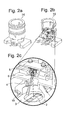
- Fig. 2 shows specific examples of optical systems in the reflection-factor measuring device of Fig. 1, Fig. 2(a) shows an outside view of the optical system, Fig. 2(b) shows a longitudinal cross-sectional view thereof, and Fig. 2(c) shows an enlarged view within the circle in Fig. 2(b).
- Fig. 3 is a drawing that shows the output characteristics of an area sensor.
- Fig. 4 is a three-dimensional contour face graph obtained when an image of a white plate is picked up by an area sensor.
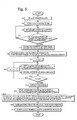
- Fig. 5 is a flow chart that shows an embodiment of a correction process of the present invention.
- Fig. 1 shows one example of a reflection-factor measuring device to which the present invention is applied.
- Fig. 2 shows specific examples of optical systems in the reflection-factor measuring device of Fig. 1
- Fig. 2(a) shows an outside view of the optical
- FIG. 6 is a plan view that shows a position of a pixel from which data is acquired.
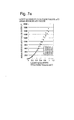
- Fig. 7 is a drawing that shows one example of correcting processes
- Fig. 7(a) is a graph that shows respective pixel outputs of an area sensor when a white plate is used as a measuring object
- Fig. 7(b) is a graph that shows an output after a PD voltage-value conversion
- Fig. 7(c) is a graph obtained when the output of Fig. 7(b) is further subjected to a light irregularity correction process.
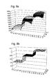
- Fig. 8 shows three-dimensional contour face graphs obtained by picking up images of a white plate in a separate manner into three stages from dark to bright in the quantity of LEDs light and aligning the pieces of image information; and Fig.
- Fig. 8(a) shows a state prior to the light-irregularity correction
- Fig. 8(b) shows a state in which the graph of Fig. 8(a) has been subjected to light-irregularity correction processes.
- Fig. 9 is a plan view that shows an example in which one sheet of an image is divided into 11 ⁇ 11 areas.
- Fig. 10 is a plan view that shows another example in which one sheet of an image is divided into 11 ⁇ 11 areas.
- Fig. 6 is a plan view that shows pixel positions that are subjected to light-irregularity corrections.
- Fig. 11 is a drawing that shows a state in which 5 points of each image shown in Fig.
- Fig. 12 is a drawing that shows the relationship between the elapsed time and temperature in main units of a reflection-factor measuring device of an embodiment.
- Fig. 13 is a drawing in which the results of measurements carried out on the reflection factor three times every 10 minutes.
- Fig. 14 is a schematic structural drawing that shows another example of the reflection-factor measuring device to which the present invention is applied.
- Fig. 15 is a drawing that shows the results of measurements carried out on standard plates having different reflection factors in the second embodiment together with the outputs of the area sensor.
- Fig. 16 is a drawing that shows the results of Fig. 15 with respect to one pixel of the area sensor.
- FIG. 17 is a flow chart that shows a sequence of processes to be carried out to obtain linearizing data in the second embodiment.
- Fig. 18 is a flow chart that shows a sequence of reflection-factor measuring processes to be carried out on an unknown sample.
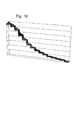
- Fig. 19 is a drawing that shows the relationship between the output of the area sensor and the exposing time, obtained as the exposing time is reduced in a third embodiment.
- Fig. 20 is a drawing that shows the results of Fig. 19 with respect to one pixel of the area sensor.
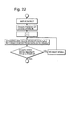
- Fig. 21 is a flow chart that shows a sequence of processes carried out to obtain linearizing data in the third embodiment.
- Fig. 22 is a flow chart that shows a sequence of reflection-factor measurements to be carried out on an unknown sample.
- Fig. 23 is a plan view that shows data-acquiring pixel positions that are used for confirming data precision after correction in the third embodiment.
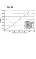
- Fig. 24 is a graph that shows the relationship between the corrected output and reflection factor in respective pixels.
- a reflection factor is measured; however, not limited to the reflection factor, the present invention may also be applied to measurements of transmittance, fluorescent light, phosphor light, chemically emitted light and the like, in the same manner.
- Fig. 1 schematically shows one example of a two-dimensional reflection-factor measuring device to which an output correction method in accordance with the first aspect of the present invention is applied with an area sensor being used as the sensor.
- Reference numeral 2 is a measuring object which is held on a sample base (not shown in Figures), and placed at a predetermined position.
- the measuring object 2 is test paper such as urine test paper and immunization measuring-use test paper, and a thin-layer chromatograph in a chemical analysis; however, in the case when an area sensor is corrected, a white plate having even reflection factor on the surface corresponds to the measuring object.
- three LEDs (light-emitting diodes) 4 serving as light sources are placed above the periphery of the measuring object 2 at the same level with 120-degree intervals from each other so as to apply light beams to the center of the measuring object 2 with an incident angle of 45 degrees.
- Each of the LEDs 4 has a center wavelength of 635 nm in its light emission.
- a CMOS area sensor 8 is placed above the measuring object 2 through an image-converging lens 6. A reflected light from the measuring object 2 is converged to form an image on the area sensor 8 by the lens 6 so that image information of the measuring object 2 is detected by the area sensor 8.
- a photodetector (PD) 10 is placed at a position out of the image angle of the area sensor 8 to sense the quantity of light from the LEDs 4.
- the photodetector 10 is prepared as a photodiode, and its output has linearity with respect to the quantity of received light, and converts the quantity of irradiated light applied to the measuring object 2 into a voltage.
- Reference numeral 12 is a voltmeter that converts the quantity of light received by the photodetector 10 into a voltage.
- a broken-line block 14 represents the fact that the LEDs 4, the lens 6, the area sensor 8 and the photodetector 10 constitute an optical system of this reflection-factor measuring device.
- a broken-line block 20 represents an area sensor drive circuit, and is provided with an amplifier 22 for amplifying an output of the area sensor 8, an A/D converter 24 for converting an amplified analog output to a digital signal, and a RAM (random-access-memory) 26 for temporarily holding an acquired digital signal.
- This area sensor drive circuit 20 controls the area sensor 8 so as to set a register for image-pickup time and to acquire image data and the like.
- the area sensor drive circuit 20 adjusts the quantity of light from the LEDs 4, carries out serial communications (56000 bps) with a personal computer 28, and executes an instruction from the personal computer 28.
- the personal computer 28 carries out various register settings of the area sensor 8, gives instructions to the area sensor drive circuit 20, acquires image information, and displays the image on a monitor. Moreover, it stores data in an appropriate format
- the personal computer 28 also achieves the above-mentioned off-set processes, linearizing processes and light-irregularity correcting processes.
- Fig. 2 shows a specific example of an optical system 14.
- Fig. 2(a) shows an outside view of the optical system
- Fig. 2(b) shows a longitudinal cross-sectional view thereof
- Fig. 2(c) shows an enlarged view within the circle in Fig. 2(b).
- This optical system has an arrangement in which the distance from the lens 6 to the measuring object 2 and the distance from the lens 6 to the area sensor 8 are finely adjusted freely; thus, it is possible to easily carry out a focusing process, a magnification-changing process and the like. Moreover, the measuring object 2 can be exchanged together with a base plate 3 of the sample base.
- the output (A/D count value) of the area sensor 8 at this time is defined as a dark (offset) state.
- a difference between the output (A/D count value) of the area sensor 8 upon irradiation by the LEDs 4 and the dark component is defined as the original output (A/D count value) of the area sensor 8.
- the relationship between the quantity of light emitted by the LEDs 4 to the measuring object 2 and the output of the area sensor 8 (count value obtained by A/D converting Vout) is not a directly proportional relationship.
- a graph shown in Fig. 3 indicates the output of the area sensor 8 obtained by varying the quantity of light from the LEDs 4, while a white plate (ND (neutral density): 9.5, actual value of reflection factor: 87.00 % (the actual value of reflection factor is measured by a spectrophotometer (MINOLTA CM-503c)(the same is true for the following measurements))) is used as the measuring object 2.
- the axis of abscissas indicates the output (mV) of a photodetector 10 placed within the optical system 14, and the axis of ordinates indicates the average value of data of appropriate 5 pixels that are successively aligned at a portion of the area sensor 8 that receives the strongest light.
- the raw image information, picked up by using this reflection-factor measuring device causes light irregularities due to influences from individual differences in sensitivity of the respective pixels in the area sensor 8, irradiation irregularities of the LEDs 4, cosine quadruple rule of the lens 6 and the like.
- a white plate (ND: 9.5, actual value of reflection factor. 87.00 %)(all the image angle range is occupied by the white plate area) is picked up, and the image information is indicated by a three-dimensional contour face graph.
- the contour face is formed by dividing the image into 10 ⁇ 10 areas and using the average value of pixels contained in each of the areas.
- the graph of Fig. 4 shows that, even in the case when an image of a flat face having even density, such as a white plate, is picked up, density information within the image angle is deformed into a dome shape due to influences from light irregularities. Processes for correcting such image information deformed into the dome shape to a horizontal face having even density are essential to a case in which the area sensor 8 is used as the photodetector in the reflection-factor measuring device. In the present invention, all the results of measurements are obtained by carrying out this light irregularity correction.
- Pixels to be corrected are five points shown in Fig. 6, which are respectively set to point 1 (32, 32), point 2 (96, 32), point 3 (64, 64), point 4 (32, 96) and point 5 (96, 96).
- Fig 7(a) shows a graph that indicates outputs at five points of the area sensor shown in Fig. 6 at the time when the quantity of light of the LEDs 4 is varied with a white plate (ND: 9.5, actual value of reflection factor 87.00 %) being used as the measuring object 2.
- Fig. 7(c) shows a graph in which the light irregularities are corrected by applying the light-irregularity correction data to Fig. 7(b).
- the respective points are plotted along virtually the same line.
- the reason that, in Fig. 7(c), five points are completely made coincident with each other when the correction output of the area sensor is 1 is because light irregularities have been corrected based on the white plate data at this brightness.
- Fig. 7(c) also shows that as the quantity of light decreases, the respective points come to deviate, resulting in degradation in correction precision.
- Fig. 8(a) shows a graph that is obtained by picking up images of the white plate (ND: 9.5, actual value of reflection factor: 87.00 %) in a manner so as to be divided three stages from dark to bright in the quantity of LEDs light (all the image angle range is occupied by the white plate area), and aligning the pieces of image information to form a three-dimensional contour face graph.
- the contour face is formed by dividing the image into 10 ⁇ 10 areas and using the average value of pixels contained in each of the areas.
- the data on the left end relates to the smallest quantity of light and the data on the right end relates to the greatest quantity of light.
- the white plate data on the right end has a narrow difference between the maximum value and the minimum value even though the quantity of light thereof is greater than that of the white plate data in the middle. This is because the pixel quantity of light at a brighter portion of the white plate is close to the saturated quantity.
- Table 1 shows the results of measurements of one time among the measurements carried out ten times.
- the upper stage of this Table shows the average of light quantities of the respective areas obtained when an image of ND 9.5 is picked up
- the intermediate stage thereof shows the average of light quantities of the respective areas obtained when an image of ND6.5 is picked up
- the lower stage thereof shows the rate of respectively identical areas that is found as the reflection factor.
- AVE represents the average value
- C. V. (%) represents a rate of change, that is, (standard deviation / average value).
- a rate of change that is, (standard deviation / average value).
- Table 2 shows the average value (upper stage) of reflection factors of the respective areas as the result of the measurements of ten times and the deviations (lower stage) in reflection factor of the respective areas.
- REFLECTION FACTOR AVERAGE (N 10) 0 10 20 30 40 50 60 70 80 90 100 110 0 10 41.08 41.05 41.44 41.23 41.20 41.22 41.40 41.86 42.21 42.99 44.09 20 41.21 41.15 41.38 41.42 41.32 41.30 41.50 41.75 42.26 43.06 43.64 30 41.10 41.29 41.34 41.50 41.39 41.35 41.33 41.60 42.04 42.80 43.53 40 41.14 41.37 41.38 41.29 41.14 41.20 41.31 41.54 41.78 42.44 43.31 50 41.05 41.32 41.37 41.24 41.02 41.13 41.09 41.40 41.62 42.27 43.00 60 41.01 41.30 41.27 41
- V. (%)(N 10) 0 10 20 30 40 50 60 70 80 90 100 110 0 10 0.758 0.687 0.629 0.567 0.540 0.613 0.557 0.551 0.580 0.615 0.625 20 0.689 0.582 0.536 0.540 0.498 0.480 0.467 0.535 0.493 0.512 0.580 30 0.608 0.588 0.510 0.469 0.409 0.400 0.386 0.376 0.416 0.417 0.486 40 0.572 0.538 0.450 0.414 0.404 0.429 0.372 0.385 0.427 0.421 0.377 50 0.566 0.524 0.429 0.386 0.402 0.404 0.394 0.455 0.422 0.417 0.420 60 0.567 0.467 0.404 0.412 0.398 0.424 0.427 0.412 0.408 0.407 0.411 70 0.530 0.542 0.396 0.426 0.417 0.424 0.427 0.388 0.433 0.411 0.423 80 0.568
- the deviation is smallest in the vicinity of the light axis of the lens 8 (or a portion in which irradiation light rays of the LEDs 4 are converged most closely), and the deviation tends to become greater as the distance from this point becomes greater in the form of a concentric circle. It is considered that this tendency occurs because the amount of correction becomes greater as the distance from the light axis becomes longer.
- Pieces of ND paper having different reflection factors were placed within the same image, and the simultaneous reproducibility, obtained in the case when the ratio of the density values of these is calculated as a reflection factor, was examined.
- the following description will discuss the sequence of the processes.
- Table 3 shows the results of measurements of one time among the measurements carried out ten times.
- the left side on the upper stage of Table 3 shows the average of light quantities of the respective areas relating to ND 9.5, and the right side on the upper stage thereof shows the average of light quantities of the respective areas relating to ND 6.5.
- the left side on the lower stage shows a case in which, supposing that a portion at which ND 9.5 and ND 6.5 intersect with each other within the image is a center line, a ratio that is found based upon this line in a line-symmetrical manner is used as a reflection factor (referred to as symmetrical reflection factor).
- the right side on the lower stage shows a case in which the area is divided into areas of ND 9.5 and ND 6.5 by the center line, with the ratio of the respectively identical areas (for example: area of lateral axis 10 and area of lateral axis 50, area of lateral axis 50 and area of lateral axis 110) being used as a reflection factor (referred to as one-directional reflection factor).
- Table 4 shows the average value (upper stage) and deviation (lower stage) obtained by carrying out calculations as shown on the lower stage of Table 3 corresponding to measurements of ten times.
- the results of simultaneous reproducibility 2 provide values that are approximately two times superior in C. V. (%) (rate of change: standard deviation / average value).
- the reason for this is because, in the measurements of simultaneous reproducibility 1, the measuring subjects need to be exchanged with the hands for each of the measurements, while, in the measurements of simultaneous reproducibility 2, it is not necessary to touch the measuring subjects with the hands. In other words, the results of simultaneous reproducibility 2 are considered to be close to the inherent image-pickup reproducibility of the CMOS area sensor.
- a known spectrophotometer (MINOLTA CM-503c: using no area sensor) whose precision had been controlled was used to measure plurality of kinds of ND paper having different reflection factors so that the correlation with the reflection factor measuring device of the embodiment of the present invention was examined.
- the reflection factors of a plurality of kinds of ND paper to be used were preliminarily measured by using the spectrophotometer. The reflection factors were measured at randomly selected five points on the ND paper, and the average value was used.
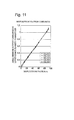
- Fig. 11 shows a graph in which values measured by the spectrophotometer are plotted on the axis of abscissas, while the five points (pixels) of each image shown in Fig. 6 are light-irregularity-corrected by the present invention and the resulting values are plotted on the axis of ordinates.
- Table 5 shows the results of all-area average reflection factor at each of the temperatures obtained by the respective measurements of ten times.
- S.D. represents the standard deviation.
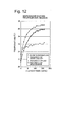
- Measurements were carried out so as to confirm the drift tendency of the reflection factor measuring device of the present embodiment in the applied state (including time and temperature).
- the graph of Fig. 12 shows the relationship between the elapsed time (every 10 minutes) and the temperature in the main units (the vicinity of the drive circuit 20, the vicinity of the LEDs 4, the vicinity of the area sensor 8) of the reflection factor measuring device of the embodiment.
- Fig. 13 shows a graph in which the resulting reflection factors, obtained by carrying out measurements three times every 10 minutes, are plotted.
- CMOS area sensor used in the present embodiment may be sufficiently applied to measurements in a semi-determination level of a measuring device for urine test paper and the like.
- Fig. 14 schematically shows one example of a two-dimensional reflection-factor measuring device to which an output correction method in accordance with the second aspect of the present invention is applied with an area sensor being used as a sensor.
- the present device is different in that a photodetector 10 for monitoring the quantity of light is not installed.
- the other structure is basically the same.
- Reflected light of a measuring object 2 is converged on an area sensor 8a as an image by a lens 6 through a reflection plate 5.
- the area sensor 8a includes devices up to the amplifier 22 shown in Fig. 1.
- the detection signal of the area sensor 8a is taken into a calculation unit 28a through an A/D converter 24.
- This calculation unit 28a corresponds to the RAM 26 and the personal computer 28 in Fig. 1.
- a display device 30, a keyboard 32 and a printer 34 are connected to the calculation unit 28a.
- Reference numeral 36 represents an image storing unit for storing acquired image data, which is constituted by, for example, a hard disk device.
- Calibration curve data 40 which is used for converting the reflection factor calculated by the calculation unit 28a to density, is stored in the hard disk device or a floppy disk device.
- the results of the data processing in the calculation unit 28a are taken out to a necessary external device as an external output 38.
- a reference plate having a known reflection factor is measured as the measuring object 2.
- pieces of ND paper are used, and those of 11 stages are prepared ranging one plate having the greatest reflection factor to another plate having the smallest reflection factor.
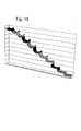
- Fig. 15 shows the results of measurements using those standard plates as the measuring object 2 together with the output of the area sensor 8a.
- the axis of ordinates represents the output
- the axis of abscesses represents the respective standard plates that are successively aligned in a descending order in the reflection factor. Since the output data of each standard plate has not been subjected to light-irregularity correcting processes, it has a curved shape.
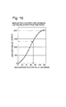
- Fig. 16 shows the relationship between the reflection factor and the output with respect to one pixel of the area sensor 8a.
- the axis of ordinates represents the output of the area sensor 8a
- the axis of abscissas represents known reflection factors of the standard plates. Since the output of the area sensor 8a has a non-linear property with respect to the quantity of received light, this curve exhibits an S-letter shape, which indicates the same characteristics as those shown in Fig. 3.
- data as shown in Fig. 16 is stored as linearizing data for each pixel.
- the reflection factor is found from its output as shown by arrows in Fig. 16.
- the reflection factor is obtained by interpolating gaps between the actually measured points of the linearizing data.
- the reflection factor of the unknown sample thus obtained is allowed to form reflection factor data in which irradiation irregularities due to a light source and non-linear properties of the lens and the area sensor 8a have been corrected, thereby preparing reflection-factor-related data having linearity.
- Fig. 17 shows a sequence used for obtaining linearizing data.
- N-number of kinds of plates having different reflection factors are prepared as reference plates.
- 11 kinds that have varied reflection factors ranging from 100 % to 0 % on a 10 % unit basis are prepared.
- One reference plate is placed at the position of the measuring object 2, and an image thereof is picked up by the area sensor 8a.
- the known reflection factor r and image-pickup data of the reference plate are stored. These operations are repeated with respect to all the reference plates.
- a sample whose reflection factor is unknown is placed at the position of the measuring object, and an image thereof is picked up by the area sensor 8a. Based upon the results of the picked up image, with respect to the coordinates (x, y) indicating the pixel position, the reflection factor is found from the output data of each pixel, in a manner as indicated by arrows in Fig. 16. These operations are carried out with respect to all the pixels.
- the reflection factor measuring device to be used is the same as that shown in Fig. 14.
- the area sensor 8a is designed so that the exposing time during which the area sensor 8a receives light is programmable.
- a CMOS image sensor H64283FP
- Mitsubishi Electric Corporation which is used in the embodiment shown in Fig. 1
- a CCD image sensor may be used as the area sensor 8a as long as it makes the exposing time programmable.
- the quantity of received light is directly proportional to the exposing time.
- the quantity of received light is directly proportional to the reflection factor, therefore, even in the case of using a single reference plate, that is, a common reference plate, by changing the exposing time, it becomes possible to obtain the same results as the measurements using reference plates having different reflection factors.
- a white plate serving as a reference plate is placed at the position of the measuring object 2 in Fig. 14. First, measurements are carried out by using reference exposing time. Next, while the white plate serving as the measuring object is maintained in the same state, the same measurements are carried out while the exposing time is reduced to 90 % of the reference exposing time. In the same manner, the exposing time is reduced to 80 %, 70 % and so on.
- Fig. 19 shows the relationship between the output (axis of ordinates) of the area sensor 8a and the exposing time (axis of abscissas, with the exposing time being shorter toward the right side) when the exposing time is reduced. In this case also, since no light-irregularity correction is carried out within the area sensor 8a, the output between pixels is varied.
- Fig. 20 shows the relationship between the output and the exposing time with respect to each of the pixels, and the same results as those of Fig. 16 and Fig. 3 are obtained.
- the data shown in Fig. 20 is stored as linearizing data with respect to each of the pixels.
- Fig. 21 shows the sequence for acquiring the linearizing data in a collective manner.
- the reference white plate is set as the measuring object 2, with the reference exposing time t being set.
- An image-pickup process is carried out by the area sensor 8a while light is applied during the corresponding exposing time so that the exposing time t and the image-pickup data are stored.
- the same measurements are repeated with the exposing time being reduced by 10 %.
- the measurements are repeatedly carried out with the exposing time being successively reduced; thus, the relationship between the sensor output and the exposing time with respect to each of the pixels is shown in Fig. 20.
- the exposing time on the axis of abscissas corresponds to the reflection factor.
- Fig. 22 shows a sequence of processes to be used for measuring a sample whose reflection factor is unknown, and this sequence is the same as that shown in Fig. 18.
- the exposing time corresponding to the reflection factor is obtained with respect to each of the pixels.
- Fig. 24 shows the relationship between the corrected output and the reflection factor with respect to each of the pixels.
- the pixel output at each position may be an output from a single pixel or an average value of the outputs from some pixels in the vicinity of the position.
- the straight line represents the average value of all the pixels.
- the axis of abscissas represents the known reflection factor
- the axis of ordinates represents the corrected output.
- the correction method of the present invention is applied to various fields such as clinical inspection, food analyses and chemical analyses as a correction method for a sensor output in various analyzers including a dry chemistry analyzer in which a test sample bearing a reagent portion on its supporting member is used.
Landscapes
- Physics & Mathematics (AREA)
- General Physics & Mathematics (AREA)
- Spectroscopy & Molecular Physics (AREA)
- Health & Medical Sciences (AREA)
- Life Sciences & Earth Sciences (AREA)
- Chemical & Material Sciences (AREA)
- Analytical Chemistry (AREA)
- Biochemistry (AREA)
- General Health & Medical Sciences (AREA)
- Immunology (AREA)
- Pathology (AREA)
- Investigating Or Analysing Materials By Optical Means (AREA)
- Photometry And Measurement Of Optical Pulse Characteristics (AREA)
- Indication And Recording Devices For Special Purposes And Tariff Metering Devices (AREA)
Abstract
Description

| REFLECTION FACTOR AVERAGE (N = 10) | ||||||||||||
| 0 | 10 | 20 | 30 | 40 | 50 | 60 | 70 | 80 | 90 | 100 | 110 | |
| 0 | ||||||||||||
| 10 | 41.08 | 41.05 | 41.44 | 41.23 | 41.20 | 41.22 | 41.40 | 41.86 | 42.21 | 42.99 | 44.09 | |
| 20 | 41.21 | 41.15 | 41.38 | 41.42 | 41.32 | 41.30 | 41.50 | 41.75 | 42.26 | 43.06 | 43.64 | |
| 30 | 41.10 | 41.29 | 41.34 | 41.50 | 41.39 | 41.35 | 41.33 | 41.60 | 42.04 | 42.80 | 43.53 | |
| 40 | 41.14 | 41.37 | 41.38 | 41.29 | 41.14 | 41.20 | 41.31 | 41.54 | 41.78 | 42.44 | 43.31 | |
| 50 | 41.05 | 41.32 | 41.37 | 41.24 | 41.02 | 41.13 | 41.09 | 41.40 | 41.62 | 42.27 | 43.00 | |
| 60 | 41.01 | 41.30 | 41.27 | 41.16 | 41.10 | 41.08 | 41.16 | 41.37 | 41.59 | 42.17 | 42.84 | |
| 70 | 40.98 | 41.18 | 41.25 | 41.19 | 41.11 | 40.96 | 41.11 | 41.38 | 41.72 | 42.05 | 42.75 | |
| 80 | 41.01 | 41.35 | 41.27 | 41.11 | 41.10 | 41.09 | 40.93 | 41.27 | 41.60 | 41.90 | 42.64 | |
| 90 | 41.05 | 41.33 | 41.42 | 41.29 | 41.00 | 41.06 | 40.96 | 41.15 | 41.60 | 42.18 | 42.79 | |
| 100 | 41.02 | 41.11 | 41.44 | 41.47 | 41.17 | 40.88 | 41.00 | 41.09 | 41.73 | 42.25 | 42.96 | |
| 110 | 40.95 | 41.10 | 41.32 | 41.38 | 41.12 | 41.16 | 41.22 | 41.20 | 41.67 | 42.49 | 43.36 | |
| 120 | ||||||||||||
| ALL AREAS 41.57 | ||||||||||||
| REFLECTION FACTOR DEVIATION C. V. (%)(N = 10) | ||||||||||||
| 0 | 10 | 20 | 30 | 40 | 50 | 60 | 70 | 80 | 90 | 100 | 110 | |
| 0 | ||||||||||||
| 10 | 0.758 | 0.687 | 0.629 | 0.567 | 0.540 | 0.613 | 0.557 | 0.551 | 0.580 | 0.615 | 0.625 | |
| 20 | 0.689 | 0.582 | 0.536 | 0.540 | 0.498 | 0.480 | 0.467 | 0.535 | 0.493 | 0.512 | 0.580 | |
| 30 | 0.608 | 0.588 | 0.510 | 0.469 | 0.409 | 0.400 | 0.386 | 0.376 | 0.416 | 0.417 | 0.486 | |
| 40 | 0.572 | 0.538 | 0.450 | 0.414 | 0.404 | 0.429 | 0.372 | 0.385 | 0.427 | 0.421 | 0.377 | |
| 50 | 0.566 | 0.524 | 0.429 | 0.386 | 0.402 | 0.404 | 0.394 | 0.455 | 0.422 | 0.417 | 0.420 | |
| 60 | 0.567 | 0.467 | 0.404 | 0.412 | 0.398 | 0.424 | 0.427 | 0.412 | 0.408 | 0.407 | 0.411 | |
| 70 | 0.530 | 0.542 | 0.396 | 0.426 | 0.417 | 0.424 | 0.427 | 0.388 | 0.433 | 0.411 | 0.423 | |
| 80 | 0.568 | 0.539 | 0.431 | 0.431 | 0.406 | 0.397 | 0.462 | 0.401 | 0.418 | 0.426 | 0.431 | |
| 90 | 0.516 | 0.567 | 0.438 | 0.427 | 0.430 | 0.433 | 0.433 | 0.420 | 0.419 | 0.405 | 0.427 | |
| 100 | 0.581 | 0.536 | 0.465 | 0.382 | 0.384 | 0.421 | 0.437 | 0.443 | 0.442 | 0.414 | 0.403 | |
| 110 | 0.650 | 0.588 | 0.571 | 0.459 | 0.392 | 0.401 | 0.414 | 0.422 | 0.422 | 0.440 | 0.442 |


Claims (12)
- A correction method for a sensor output, which applies light to a measuring object and carries out measurements by receiving light reflected from a detection subject portion by a sensor, whereinsaid sensor lacking linearity in an output thereof in response to the quantity of received light, andsaid method comprises a linearizing process that corrects the sensor output so that the output from said sensor in response to a variation in the quantity of received light is made proportional to the quantity of received light.
- The correction method for a sensor output according to claim 1, wherein said linearizing process comprises the following processes (A) and (B):(A) a process in which a photodetector having linearity in an output thereof in response to the quantity of received light is arranged so that light to be made incident on the sensor is simultaneously made incident on said photodetector, and upon variation in the quantity of incident light, a relationship between the sensor output and the output of said photodetector is stored as linearizing data; and(B) a process in which, upon measurement of a measuring object, the resulting sensor output is corrected and made proportional to the output of said photodetector based upon said linearizing data.
- The correction method for a sensor output according to claim 1, wherein said linearizing process comprises the following processes (A) and (B):(A) a process in which using a plurality of standard plates having known reflection light rays that are respectively different from each other, a relationship between the output from said sensor obtained when each of the standard plates is measured and the light from the standard plate is stored as linearizing data; and(B) a process in which, upon measurement of a measuring object, the resulting sensor output is corrected and made proportional to the light ray from said standard plate based upon said linearizing data.
- The correction method for a sensor output according to claim 1, wherein said linearizing process comprises the following processes (A) and (B):(A) a process in which said sensor is allowed to variably set exposing time, and upon measuring one reference object, a relationship between each of said sensor outputs obtained from measurements carried out while changing the exposing time in a plurality of stages and the corresponding exposing time is stored as linearizing data relating to light from the reference object, which is proportional to the exposing time, and(B) a process in which the sensor output, obtained upon measuring a measuring object, is corrected so as to be made proportional to light from the reference object that is found by the exposing time based upon the linearizing data.
- The correction method for a sensor output according to any of claims 1 to 4, wherein said sensor is an area sensor and said linearizing process is carried out on each of said pixels.
- The correction method for a sensor output according to any of claims 1 to 4, wherein said sensor is an area sensor, and said linearizing process is carried out by selecting some pixels in the vicinity of the brightest pixel within the image and using the average value of outputs of these pixels.
- The correction method for a sensor output according to claim 5 or claim 6, wherein a CCD or CMOS sensor is used as said area sensor.
- The correction method for a sensor output according to any of claims 1 to 7, wherein said sensor output corresponds to a value that is obtained after an offset process by subtracting an output at the time when the quantity of received light is zero as dark data from the output.
- The correction method for a sensor output according to any of claims 5 to 8, further comprising a light-irregularity correction process which, after a reference object has been measured as a measuring object, corrects the outputs of the respective pixels so that corrected values, obtained by subjecting the corresponding outputs of the respective pixels of said area sensor to said linearizing process, are evenly adjusted.
- The correction method for a sensor output according to any of claims 5 to 9, wherein a reference object is measured as a measuring object, and said light-irregularity correction process is carried out on image data by using a quantity of received light at a fixed ratio close to the saturated quantity of light with respect to the quantity of received light at the time when the pixel has reached a saturated quantity of light.
- The correction method for a sensor output according to claim 4, claim 9 or claim 10, wherein said reference object is a reflection plate having even in-plane density or a blank.
- The correction method for a sensor output according to claim 2, wherein a photodiode is used as said photodetector whose output has linearity with respect to quantity of received light.
Applications Claiming Priority (3)
| Application Number | Priority Date | Filing Date | Title |
|---|---|---|---|
| JP2000343365 | 2000-11-10 | ||
| JP2000343365 | 2000-11-10 | ||
| PCT/JP2001/009850 WO2002039076A1 (en) | 2000-11-10 | 2001-11-09 | Method for correcting sensor output |
Publications (3)
| Publication Number | Publication Date |
|---|---|
| EP1333258A1 true EP1333258A1 (en) | 2003-08-06 |
| EP1333258A4 EP1333258A4 (en) | 2011-04-06 |
| EP1333258B1 EP1333258B1 (en) | 2013-08-21 |
Family
ID=18817743
Family Applications (1)
| Application Number | Title | Priority Date | Filing Date |
|---|---|---|---|
| EP01982755.9A Expired - Lifetime EP1333258B1 (en) | 2000-11-10 | 2001-11-09 | Method for correcting sensor output |
Country Status (6)
| Country | Link |
|---|---|
| US (1) | US7110901B2 (en) |
| EP (1) | EP1333258B1 (en) |
| JP (1) | JP3754989B2 (en) |
| CN (1) | CN1241000C (en) |
| AU (1) | AU2002214275A1 (en) |
| WO (1) | WO2002039076A1 (en) |
Cited By (1)
| Publication number | Priority date | Publication date | Assignee | Title |
|---|---|---|---|---|
| CN101233395B (en) * | 2005-06-08 | 2012-01-11 | 罗斯蒙德公司 | Process field device with infrared sensors |
Families Citing this family (18)
| Publication number | Priority date | Publication date | Assignee | Title |
|---|---|---|---|---|
| CA2601720C (en) * | 2005-04-01 | 2014-08-12 | Advanced Medical Products Gmbh | Body fluid testing component for analyte detection |
| DE102007002106B3 (en) * | 2007-01-09 | 2008-07-03 | Wolfgang Weinhold | Object's surface configuration examining device, has control and evaluation unit connected with light sources and light sensor, where light sources are arranged such that optical radiation axis runs in different reference planes |
| EP2073055A1 (en) * | 2007-12-20 | 2009-06-24 | TPO Displays Corp. | Detection of an incident light distribution |
| RU2420728C2 (en) * | 2009-06-26 | 2011-06-10 | Закрытое акционерное общество Научно-производственное объединение "Гранит-НЭМП" | Method of correcting output signal of photometric sensor |
| JP5275956B2 (en) * | 2009-10-15 | 2013-08-28 | 株式会社ジャパンディスプレイウェスト | Information input device, information input program, and electronic device |
| JP5387979B2 (en) * | 2009-12-20 | 2014-01-15 | 独立行政法人産業技術総合研究所 | Linearity inspection apparatus and linearity inspection method |
| US20140152771A1 (en) * | 2012-12-01 | 2014-06-05 | Og Technologies, Inc. | Method and apparatus of profile measurement |
| CN103925992B (en) * | 2013-01-16 | 2016-03-16 | 光宝电子(广州)有限公司 | There are the brightness measurement method and system of the device of backlight |
| CN104019902B (en) * | 2014-06-16 | 2016-09-28 | 武汉工程大学 | Household test paper reader device and detection method thereof |
| CN106197667A (en) * | 2016-07-12 | 2016-12-07 | 江苏浦亚照明科技股份有限公司 | A kind of miniature multi-channel spectrogrph and the Nonlinearity Correction Method of detector thereof |
| JP6841406B2 (en) | 2016-09-09 | 2021-03-10 | 大塚電子株式会社 | Optical measurement method and optical measurement device |
| DE102017110269A1 (en) * | 2017-05-11 | 2018-11-15 | B. Braun Avitum Ag | Online linearization of an optical sensor |
| US10429174B2 (en) * | 2017-12-20 | 2019-10-01 | Texas Instruments Incorporated | Single wavelength reflection for leadframe brightness measurement |
| CN109668847A (en) * | 2019-02-14 | 2019-04-23 | 杭州霆科生物科技有限公司 | A kind of residual tacheometer of agriculture with optics self-calibration function |
| US11733605B2 (en) * | 2019-06-20 | 2023-08-22 | Kla Corporation | EUV in-situ linearity calibration for TDI image sensors using test photomasks |
| CN110519516B (en) * | 2019-08-30 | 2020-09-25 | 联想(北京)有限公司 | Image noise processing method and device and electronic equipment |
| JP7419029B2 (en) * | 2019-11-14 | 2024-01-22 | 大塚電子株式会社 | Linearity correction method for optical measurement device, optical measurement method, and optical measurement device |
| CN111256744B (en) * | 2020-02-27 | 2021-06-29 | 苏州海之博电子科技有限公司 | Calibration method of linear output position sensor |
Family Cites Families (13)
| Publication number | Priority date | Publication date | Assignee | Title |
|---|---|---|---|---|
| JPH03204285A (en) * | 1989-12-29 | 1991-09-05 | Nec Corp | Uneven sensitivity correction circuit for solid-state image pickup element |
| JPH03289777A (en) * | 1990-04-05 | 1991-12-19 | Nec Corp | Infrared image pickup device |
| US5229838A (en) * | 1992-01-21 | 1993-07-20 | The Perkin-Elmer Corporation | Photodetector amplitude linearity |
| JPH05297142A (en) * | 1992-04-21 | 1993-11-12 | Toshiba Corp | Scintillation camera |
| JPH06225143A (en) | 1993-01-27 | 1994-08-12 | Tokyo Electric Co Ltd | Image reader |
| JPH08128922A (en) * | 1994-10-31 | 1996-05-21 | Asahi Optical Co Ltd | Digital data processor |
| GB2314227B (en) | 1996-06-14 | 1998-12-23 | Simage Oy | Calibration method and system for imaging devices |
| US5902994A (en) * | 1997-05-06 | 1999-05-11 | Eastman Kodak Company | Apparatus for calibrating a linear image sensor |
| JPH11249004A (en) * | 1998-03-02 | 1999-09-17 | Nikon Corp | Image sensor |
| US6147702A (en) | 1998-04-17 | 2000-11-14 | Intel Corporation | Calibration of digital cameras |
| JP3863290B2 (en) | 1998-05-12 | 2006-12-27 | 浜松ホトニクス株式会社 | Light intensity detector |
| JP2000013807A (en) * | 1998-06-24 | 2000-01-14 | Seiko Epson Corp | Digital camera |
| EP1333273A4 (en) * | 2000-11-10 | 2011-04-06 | Arkray Inc | Measuring method and instrument comprising image sensor |
-
2001
- 2001-11-09 JP JP2002541352A patent/JP3754989B2/en not_active Expired - Lifetime
- 2001-11-09 US US10/415,991 patent/US7110901B2/en not_active Expired - Lifetime
- 2001-11-09 EP EP01982755.9A patent/EP1333258B1/en not_active Expired - Lifetime
- 2001-11-09 CN CN01818683.1A patent/CN1241000C/en not_active Expired - Lifetime
- 2001-11-09 AU AU2002214275A patent/AU2002214275A1/en not_active Abandoned
- 2001-11-09 WO PCT/JP2001/009850 patent/WO2002039076A1/en not_active Ceased
Cited By (1)
| Publication number | Priority date | Publication date | Assignee | Title |
|---|---|---|---|---|
| CN101233395B (en) * | 2005-06-08 | 2012-01-11 | 罗斯蒙德公司 | Process field device with infrared sensors |
Also Published As
| Publication number | Publication date |
|---|---|
| US20040034494A1 (en) | 2004-02-19 |
| AU2002214275A1 (en) | 2002-05-21 |
| WO2002039076A1 (en) | 2002-05-16 |
| JPWO2002039076A1 (en) | 2004-03-18 |
| CN1241000C (en) | 2006-02-08 |
| EP1333258B1 (en) | 2013-08-21 |
| CN1474937A (en) | 2004-02-11 |
| JP3754989B2 (en) | 2006-03-15 |
| EP1333258A4 (en) | 2011-04-06 |
| US7110901B2 (en) | 2006-09-19 |
Similar Documents
| Publication | Publication Date | Title |
|---|---|---|
| US7110901B2 (en) | Correction method for sensor output | |
| US7274829B2 (en) | Measuring method and instrument comprising image sensor | |
| US7443508B1 (en) | Spectrophotometric scanner | |
| CN112334759B (en) | A method for detecting an analyte in a sample | |
| JP3628727B2 (en) | Video test strip reader and test strip evaluation method | |
| US7928354B2 (en) | Methods and systems for in situ calibration of imaging in biological analysis | |
| US20100239137A1 (en) | Two Dimensional Imaging of Reacted Areas On a Reagent | |
| US20160069808A1 (en) | Fluorescence imaging autofocus systems and methods | |
| JPS63298101A (en) | Non-contact determination method and apparatus for position of linear feature of article | |
| JPH0758263B2 (en) | Analytical method using automatic fluorometer | |
| EP1904954A2 (en) | Method of extracting intensity data from digitized image | |
| US20200408916A1 (en) | Distance measurement device having external light illuminance measurement function and external light illuminance measurement method | |
| JP2009109315A (en) | Optical measuring device and scanning optical system | |
| JP2009222607A (en) | Illumination control method of sample analyzer, and sample analyzer | |
| CN216560316U (en) | Integrating sphere structure based on arbitrary spectrum and calibration equipment | |
| CN115097135B (en) | Fluorescence test paper quantitative analyzer | |
| JP2024165391A (en) | Biological sample measuring device and calibration method | |
| JP3873088B2 (en) | Optical inspection device | |
| JPH0332984Y2 (en) | ||
| JP2023094872A (en) | Computer program, spectroscopic device, and spectroscopic method | |
| JPS60108731A (en) | Measured-value correcting method of automatic analyzing apparatus | |
| JPH09105669A (en) | Image processing apparatus and image processing method for detecting a trace amount of adhesion | |
| JPS63205529A (en) | Infrared image pickup device | |
| WO2001009588A1 (en) | Method and apparatus to reduce reflectance errors due to non-uniform color development | |
| JPH0783095B2 (en) | Inspection method for solid-state image sensor |
Legal Events
| Date | Code | Title | Description |
|---|---|---|---|
| PUAI | Public reference made under article 153(3) epc to a published international application that has entered the european phase |
Free format text: ORIGINAL CODE: 0009012 |
|
| 17P | Request for examination filed |
Effective date: 20030508 |
|
| AK | Designated contracting states |
Designated state(s): AT BE CH CY DE DK ES FI FR GB GR IE IT LI LU MC NL PT SE TR |
|
| AX | Request for extension of the european patent |
Extension state: AL LT LV MK RO SI |
|
| REG | Reference to a national code |
Ref country code: DE Ref legal event code: R079 Ref document number: 60148268 Country of ref document: DE Free format text: PREVIOUS MAIN CLASS: G01J0001440000 Ipc: G01N0021000000 |
|
| A4 | Supplementary search report drawn up and despatched |
Effective date: 20110307 |
|
| RIC1 | Information provided on ipc code assigned before grant |
Ipc: G01N 21/59 20060101ALI20110301BHEP Ipc: G01J 1/16 20060101ALI20110301BHEP Ipc: G01N 21/00 20060101AFI20110301BHEP Ipc: G01J 1/12 20060101ALI20110301BHEP |
|
| 17Q | First examination report despatched |
Effective date: 20110705 |
|
| GRAP | Despatch of communication of intention to grant a patent |
Free format text: ORIGINAL CODE: EPIDOSNIGR1 |
|
| GRAS | Grant fee paid |
Free format text: ORIGINAL CODE: EPIDOSNIGR3 |
|
| GRAA | (expected) grant |
Free format text: ORIGINAL CODE: 0009210 |
|
| AK | Designated contracting states |
Kind code of ref document: B1 Designated state(s): AT BE CH CY DE DK ES FI FR GB GR IE IT LI LU MC NL PT SE TR |
|
| REG | Reference to a national code |
Ref country code: GB Ref legal event code: FG4D |
|
| REG | Reference to a national code |
Ref country code: CH Ref legal event code: EP |
|
| REG | Reference to a national code |
Ref country code: AT Ref legal event code: REF Ref document number: 628364 Country of ref document: AT Kind code of ref document: T Effective date: 20130915 |
|
| REG | Reference to a national code |
Ref country code: IE Ref legal event code: FG4D |
|
| REG | Reference to a national code |
Ref country code: DE Ref legal event code: R096 Ref document number: 60148268 Country of ref document: DE Effective date: 20131017 |
|
| REG | Reference to a national code |
Ref country code: NL Ref legal event code: VDEP Effective date: 20130821 Ref country code: AT Ref legal event code: MK05 Ref document number: 628364 Country of ref document: AT Kind code of ref document: T Effective date: 20130821 |
|
| PG25 | Lapsed in a contracting state [announced via postgrant information from national office to epo] |
Ref country code: PT Free format text: LAPSE BECAUSE OF FAILURE TO SUBMIT A TRANSLATION OF THE DESCRIPTION OR TO PAY THE FEE WITHIN THE PRESCRIBED TIME-LIMIT Effective date: 20131223 Ref country code: CY Free format text: LAPSE BECAUSE OF FAILURE TO SUBMIT A TRANSLATION OF THE DESCRIPTION OR TO PAY THE FEE WITHIN THE PRESCRIBED TIME-LIMIT Effective date: 20130619 Ref country code: AT Free format text: LAPSE BECAUSE OF FAILURE TO SUBMIT A TRANSLATION OF THE DESCRIPTION OR TO PAY THE FEE WITHIN THE PRESCRIBED TIME-LIMIT Effective date: 20130821 Ref country code: SE Free format text: LAPSE BECAUSE OF FAILURE TO SUBMIT A TRANSLATION OF THE DESCRIPTION OR TO PAY THE FEE WITHIN THE PRESCRIBED TIME-LIMIT Effective date: 20130821 |
|
| PG25 | Lapsed in a contracting state [announced via postgrant information from national office to epo] |
Ref country code: GR Free format text: LAPSE BECAUSE OF FAILURE TO SUBMIT A TRANSLATION OF THE DESCRIPTION OR TO PAY THE FEE WITHIN THE PRESCRIBED TIME-LIMIT Effective date: 20131122 Ref country code: FI Free format text: LAPSE BECAUSE OF FAILURE TO SUBMIT A TRANSLATION OF THE DESCRIPTION OR TO PAY THE FEE WITHIN THE PRESCRIBED TIME-LIMIT Effective date: 20130821 Ref country code: BE Free format text: LAPSE BECAUSE OF FAILURE TO SUBMIT A TRANSLATION OF THE DESCRIPTION OR TO PAY THE FEE WITHIN THE PRESCRIBED TIME-LIMIT Effective date: 20130821 |
|
| PG25 | Lapsed in a contracting state [announced via postgrant information from national office to epo] |
Ref country code: CY Free format text: LAPSE BECAUSE OF FAILURE TO SUBMIT A TRANSLATION OF THE DESCRIPTION OR TO PAY THE FEE WITHIN THE PRESCRIBED TIME-LIMIT Effective date: 20130821 |
|
| PG25 | Lapsed in a contracting state [announced via postgrant information from national office to epo] |
Ref country code: NL Free format text: LAPSE BECAUSE OF FAILURE TO SUBMIT A TRANSLATION OF THE DESCRIPTION OR TO PAY THE FEE WITHIN THE PRESCRIBED TIME-LIMIT Effective date: 20130821 Ref country code: DK Free format text: LAPSE BECAUSE OF FAILURE TO SUBMIT A TRANSLATION OF THE DESCRIPTION OR TO PAY THE FEE WITHIN THE PRESCRIBED TIME-LIMIT Effective date: 20130821 |
|
| PG25 | Lapsed in a contracting state [announced via postgrant information from national office to epo] |
Ref country code: ES Free format text: LAPSE BECAUSE OF FAILURE TO SUBMIT A TRANSLATION OF THE DESCRIPTION OR TO PAY THE FEE WITHIN THE PRESCRIBED TIME-LIMIT Effective date: 20130821 |
|
| PLBE | No opposition filed within time limit |
Free format text: ORIGINAL CODE: 0009261 |
|
| STAA | Information on the status of an ep patent application or granted ep patent |
Free format text: STATUS: NO OPPOSITION FILED WITHIN TIME LIMIT |
|
| REG | Reference to a national code |
Ref country code: CH Ref legal event code: PL |
|
| 26N | No opposition filed |
Effective date: 20140522 |
|
| PG25 | Lapsed in a contracting state [announced via postgrant information from national office to epo] |
Ref country code: LI Free format text: LAPSE BECAUSE OF NON-PAYMENT OF DUE FEES Effective date: 20131130 Ref country code: MC Free format text: LAPSE BECAUSE OF FAILURE TO SUBMIT A TRANSLATION OF THE DESCRIPTION OR TO PAY THE FEE WITHIN THE PRESCRIBED TIME-LIMIT Effective date: 20130821 Ref country code: CH Free format text: LAPSE BECAUSE OF NON-PAYMENT OF DUE FEES Effective date: 20131130 |
|
| REG | Reference to a national code |
Ref country code: IE Ref legal event code: MM4A |
|
| REG | Reference to a national code |
Ref country code: DE Ref legal event code: R097 Ref document number: 60148268 Country of ref document: DE Effective date: 20140522 |
|
| PG25 | Lapsed in a contracting state [announced via postgrant information from national office to epo] |
Ref country code: IE Free format text: LAPSE BECAUSE OF NON-PAYMENT OF DUE FEES Effective date: 20131109 |
|
| PG25 | Lapsed in a contracting state [announced via postgrant information from national office to epo] |
Ref country code: TR Free format text: LAPSE BECAUSE OF FAILURE TO SUBMIT A TRANSLATION OF THE DESCRIPTION OR TO PAY THE FEE WITHIN THE PRESCRIBED TIME-LIMIT Effective date: 20130821 |
|
| PG25 | Lapsed in a contracting state [announced via postgrant information from national office to epo] |
Ref country code: LU Free format text: LAPSE BECAUSE OF NON-PAYMENT OF DUE FEES Effective date: 20131109 |
|
| REG | Reference to a national code |
Ref country code: FR Ref legal event code: PLFP Year of fee payment: 15 |
|
| REG | Reference to a national code |
Ref country code: FR Ref legal event code: PLFP Year of fee payment: 16 |
|
| REG | Reference to a national code |
Ref country code: FR Ref legal event code: PLFP Year of fee payment: 17 |
|
| PGFP | Annual fee paid to national office [announced via postgrant information from national office to epo] |
Ref country code: GB Payment date: 20201120 Year of fee payment: 20 Ref country code: DE Payment date: 20201119 Year of fee payment: 20 Ref country code: FR Payment date: 20201120 Year of fee payment: 20 Ref country code: IT Payment date: 20201124 Year of fee payment: 20 |
|
| REG | Reference to a national code |
Ref country code: DE Ref legal event code: R071 Ref document number: 60148268 Country of ref document: DE |
|
| REG | Reference to a national code |
Ref country code: GB Ref legal event code: PE20 Expiry date: 20211108 |
|
| PG25 | Lapsed in a contracting state [announced via postgrant information from national office to epo] |
Ref country code: GB Free format text: LAPSE BECAUSE OF EXPIRATION OF PROTECTION Effective date: 20211108 |