EP1331695A2 - Elektronische Baugruppe - Google Patents
Elektronische Baugruppe Download PDFInfo
- Publication number
- EP1331695A2 EP1331695A2 EP02025306A EP02025306A EP1331695A2 EP 1331695 A2 EP1331695 A2 EP 1331695A2 EP 02025306 A EP02025306 A EP 02025306A EP 02025306 A EP02025306 A EP 02025306A EP 1331695 A2 EP1331695 A2 EP 1331695A2
- Authority
- EP
- European Patent Office
- Prior art keywords
- contact
- press
- circuit board
- conductor
- der
- Prior art date
- Legal status (The legal status is an assumption and is not a legal conclusion. Google has not performed a legal analysis and makes no representation as to the accuracy of the status listed.)
- Withdrawn
Links
Images


Classifications
-
- H—ELECTRICITY
- H01—ELECTRIC ELEMENTS
- H01R—ELECTRICALLY-CONDUCTIVE CONNECTIONS; STRUCTURAL ASSOCIATIONS OF A PLURALITY OF MUTUALLY-INSULATED ELECTRICAL CONNECTING ELEMENTS; COUPLING DEVICES; CURRENT COLLECTORS
- H01R13/00—Details of coupling devices of the kinds covered by groups H01R12/70 or H01R24/00 - H01R33/00
- H01R13/02—Contact members
- H01R13/22—Contacts for co-operating by abutting
- H01R13/24—Contacts for co-operating by abutting resilient; resiliently-mounted
- H01R13/2442—Contacts for co-operating by abutting resilient; resiliently-mounted with a single cantilevered beam
-
- H—ELECTRICITY
- H01—ELECTRIC ELEMENTS
- H01R—ELECTRICALLY-CONDUCTIVE CONNECTIONS; STRUCTURAL ASSOCIATIONS OF A PLURALITY OF MUTUALLY-INSULATED ELECTRICAL CONNECTING ELEMENTS; COUPLING DEVICES; CURRENT COLLECTORS
- H01R12/00—Structural associations of a plurality of mutually-insulated electrical connecting elements, specially adapted for printed circuits, e.g. printed circuit boards [PCB], flat or ribbon cables, or like generally planar structures, e.g. terminal strips, terminal blocks; Coupling devices specially adapted for printed circuits, flat or ribbon cables, or like generally planar structures; Terminals specially adapted for contact with, or insertion into, printed circuits, flat or ribbon cables, or like generally planar structures
- H01R12/50—Fixed connections
- H01R12/59—Fixed connections for flexible printed circuits, flat or ribbon cables or like structures
- H01R12/62—Fixed connections for flexible printed circuits, flat or ribbon cables or like structures connecting to rigid printed circuits or like structures
-
- H—ELECTRICITY
- H05—ELECTRIC TECHNIQUES NOT OTHERWISE PROVIDED FOR
- H05K—PRINTED CIRCUITS; CASINGS OR CONSTRUCTIONAL DETAILS OF ELECTRIC APPARATUS; MANUFACTURE OF ASSEMBLAGES OF ELECTRICAL COMPONENTS
- H05K1/00—Printed circuits
- H05K1/02—Details
- H05K1/14—Structural association of two or more printed circuits
- H05K1/147—Structural association of two or more printed circuits at least one of the printed circuits being bent or folded, e.g. by using a flexible printed circuit
-
- H—ELECTRICITY
- H01—ELECTRIC ELEMENTS
- H01R—ELECTRICALLY-CONDUCTIVE CONNECTIONS; STRUCTURAL ASSOCIATIONS OF A PLURALITY OF MUTUALLY-INSULATED ELECTRICAL CONNECTING ELEMENTS; COUPLING DEVICES; CURRENT COLLECTORS
- H01R12/00—Structural associations of a plurality of mutually-insulated electrical connecting elements, specially adapted for printed circuits, e.g. printed circuit boards [PCB], flat or ribbon cables, or like generally planar structures, e.g. terminal strips, terminal blocks; Coupling devices specially adapted for printed circuits, flat or ribbon cables, or like generally planar structures; Terminals specially adapted for contact with, or insertion into, printed circuits, flat or ribbon cables, or like generally planar structures
- H01R12/50—Fixed connections
- H01R12/51—Fixed connections for rigid printed circuits or like structures
- H01R12/55—Fixed connections for rigid printed circuits or like structures characterised by the terminals
- H01R12/58—Fixed connections for rigid printed circuits or like structures characterised by the terminals terminals for insertion into holes
- H01R12/585—Terminals having a press fit or a compliant portion and a shank passing through a hole in the printed circuit board
Definitions
- the invention relates to an electronic assembly according to the preamble of claim 1 as it is known from the unpublished DE 101 57 113.
- electronic assemblies are used for different tasks and applications; in particular (e.g. in the motor vehicle sector for controlling and / or regulating driving-specific processes or comfort functions) as electronic assemblies, control units with sensors for recording the measured values of physical variables such as temperature, speed or pressure and / or with actuators for actuating Actuators in use.
- a circuit board having a conductor track structure is usually provided as the carrier body for the components of the electronic assembly;
- a conductor foil with a conductor track structure can be provided as a further carrier body for components of the electronic assembly and / or as a wiring carrier for the electrical contacting (for example for external contacting of the electronic assembly).
- an electrically conductive connection must be provided between (at least one contact point) the conductor track structure of the printed circuit board and (at least one contact point) the conductor track structure of the conductor foil; this is generally realized by means of a connector which starts from the conductor track structure of the printed circuit board and which is connected to the conductor track structure of the conductor foil by soldering or crimping and thus permanently fixed. Because of the non-releasable connection, such a connector is disadvantageous or unsuitable for many applications.
- the one for contacting the conductor track structure Press-in pins provided on the printed circuit board are molded onto the side of the contact element and can be bent at the desired angle for the press-in process; the one provided for contacting the conductor track structure of the switching film, in the middle arranged in the contact element has on its underside in the end region at least one cutting edge for exposing the conductor track structure to be contacted on the switching foil and at least one contact zone Realization of a gas-tight contact point on the circuit structure of the switching foil on. Furthermore, it is laterally adjacent on both sides along the contact zones at least one grinder to ensure a reliable press-in process arranged.
- the invention has for its object to provide an electronic assembly according to the preamble of claim 1 with a simple structure, simple manufacture, low cost, high reliability and advantageous properties with respect to the electrical connection.
- This object is achieved according to the invention by the features in the characterizing part of patent claim 1.
- Advantageous embodiments of the invention are part of the further claims.
- At least one contact element realized as a hook-shaped press-in contact (as a clamping spring or contact spring) is provided, at which the press-in pin provided for contacting the conductor track structure of the printed circuit board forms the straight section of the hook-shaped press-in contact and the contact tongue provided for contacting the conductor track structure of the conductor film forms the bent section of the hook-shaped press-in contact as a spring element.
- the electronic assembly can have any number of such press-in contacts, in particular a plurality of press-in contacts arranged one behind the other and / or next to one another.
- the press-in pin of the press-in contact which is provided for contacting the conductor track structure of the printed circuit board and thus for forming the contact point on the conductor track structure of the printed circuit board, is pressed into the printed circuit board at a specific contact point; E.g. the press-in contact is pressed into a via provided in the printed circuit board as a contact point.
- the contact tongue provided for contacting the conductor track structure of the conductor film and thus for forming the contact point on the conductor track structure of the conductor film is brought into the desired curved shape in a bending process before the pressing-in process, in particular the contact tongue is bent semicircularly; the contact tongue has on its outside, preferably in the middle of the curved section and thus in the extension of the straight section, a preferably rounded, e.g. hemispherical contact zone for realizing a gas-tight contact point on the conductor track structure of the conductor foil.
- the contact element is preferably designed as a stamped and bent part and consists of an electrically conductive material with the required spring properties for the press-in process and the bending process and thus for the electrical contacting of the conductor track structure of the printed circuit board and for the electrical contacting of the conductor track structure of the switching film of the conductor film.
- the contact element consists of a metallic alloy, in particular of a copper-containing contact material, e.g. from a copper-tin-bronze (CuSn) or from copper-nickel-silicon (CuNiSi).
- the in the pressing process in the circuit board especially in holes in the circuit board, for example. in bores formed as plated-through holes through the printed circuit board, pressed-in press-in pin of the press-in contact is contacted with the conductor track structure of the printed circuit board to form contact points;
- the contact points are formed on the top of the printed circuit board and / or on the underside of the printed circuit board and / or in the printed circuit board (in particular in the case of a multilayer printed circuit board having a plurality of conductor track levels), for example. in the area of vias through the circuit board.
- the contact tongue of the press-in contact which is bent into the desired shape before the press-in process in the bending process, protrudes as a spring element on the top of the printed circuit board after the press-in pin has been pressed in.
- the circuit board is now in an open at least on one side, for example.
- Plastic housing body introduced, which mechanically fixes the circuit board as a clamp or clamp and compresses the contact tongue of the press-in contact somewhat (pretension of the contact tongue of the press-in contact).
- the switching film of the conductor film must be accessible at least at the contacting points provided; in the case of a flexible printed circuit board as the conductor film, the conductor track structure of the switching film arranged on the carrier body serving as the insulating layer is already fully accessible; in the case of a conductor film with a switching film arranged as an insulating layer between two insulating films, one of the insulating films is at least partially removed for this purpose at the contacting points provided and thus the Switching film partially exposed on one surface side at the intended contact points.
- the conductor film is now inserted into the housing body, preferably with the aid of insertion aids (positioning aids) formed on the housing body, in such a way that the switching film of the conductor film is positioned on the upper side of the contact tongues, that is to say it lies on the contact zones of the contact tongues, and the insulation layer ( ie, for example, either the carrier body for the switching film or the completely obtained insulation film) rests on the inside of the housing body.
- Insertion aids designed as insertion grooves in the housing body ensure that the switching foil of the conductor foil is positioned as intended with respect to the contact tongues, as a result of which the contact zones of the contact tongues form contact points on the conductor track structure of the switching foil at the desired contacting points.
- the conductor track structure of the switching film consists of copper;
- the contact zone of the contact tongue preferably consists of a metal, but at least it has a metallic surface, for example. a tinned surface.
- Connection contacts for external contacting of the electronic assembly can be formed on the conductor film, for example.
- connection contacts can be applied to the switching foil of the conductor foil by crimping or welding or soldering; in particular, several connection contacts can be combined as a plug connection and, for example. can be integrated in a common connector housing.
- Suitable connection components can be connected to the connection contacts and in particular to a plug connection, in particular connection lines or connection plugs.
- the components of the circuit arrangement of the electronic assembly are applied to the printed circuit board and / or to the printed circuit film and are conductively connected to the printed circuit structure of the printed circuit board and / or the printed circuit structure of the printed film in a suitable manner.
- Figure 1 is an example. made of copper-nickel-silicon (CuNiSi), press-in contact manufactured as a stamped and bent part as contact element 4 in the initial state (in the unwound state) after stamping and before the bending process.
- the press-in contact 4 which is formed symmetrically with respect to the longitudinal axis 43, has a contact tongue 41, on the upper side 411 of which an example. embossed contact zone 42 is provided; the contact tongue 41 is bent in a bending process before the press-in contact 4 is pressed into the desired shape.
- a press-in pin 44 is integrally formed on the contact tongue 41; In order to ensure flexibility of the press-in pin 44, in particular during the press-in process, at least one recess 45 can be provided in the press-in pin 44.
- the press-in contact 4 has a total length of 6.5 mm before the bending process, the length of the press-in pin 44, for example. Is 2.5 mm; the width of the contact tongue 41 is, for example. 1.2 mm, the width of the press-in pin 44 is e.g. 0.7 mm.
- FIG. 2 FIG. 2.1 to FIG. 2.4
- the press-in contact 4 after the bending process is shown in different perspectives before the press-in process.
- the contact tongue 41 is bent approximately semicircularly and forms the bent partial area of the press-in contact 4, the contact zone 42 arranged on the upper side 411 of the contact tongue 41 being located centrally in the bent partial area of the contact tongue 41; the press-in pin 44, on the other hand, is not bent over and forms the straight section of the press-in contact 4, so that the press-in contact 4 has a hook-like shape after the bending process.
- the press-in contact 4 has a total height of 3.6 mm after the bending process; the total length of the press-in contact 4 after the bending process 41 is, for example. 2.6 mm, the length of the press-in pin 44 is e.g. 0.35 mm.
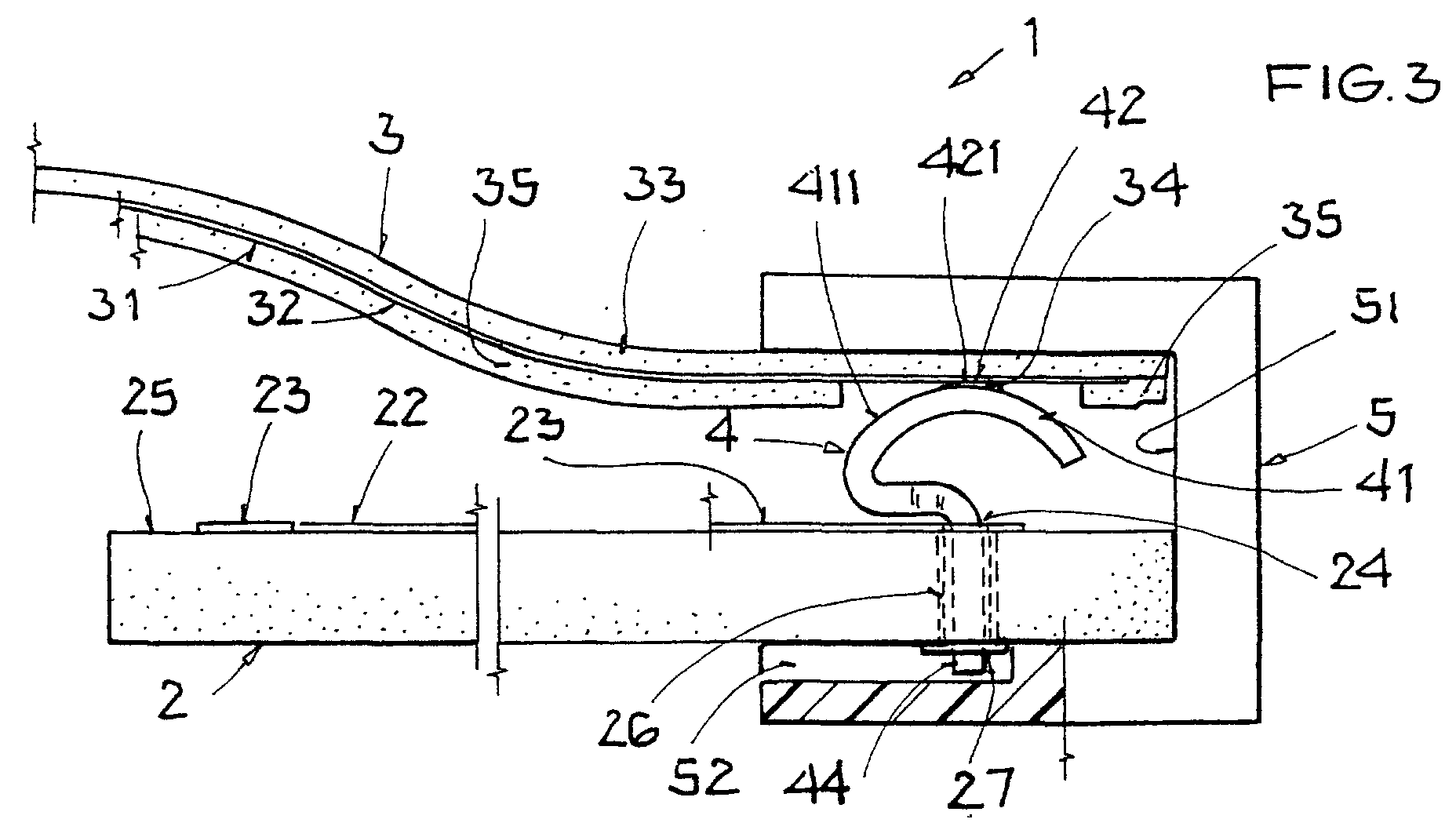
- FIG. 3 shows a sectional drawing of the composite of printed circuit board 2 and conductive film 3 after the press-in process of press-in contact 4 and insertion of conductive film 3 and thus after electrical contacting of printed circuit board 2 and conductive film 3 by press-in contact 4.
- the circuit board 2 has on the top 25 a conductor track structure 22 with conductor tracks (connecting lines) 23; furthermore, plated-through holes 26 are provided in the printed circuit board 2 as contact points for forming contact points 24.
- the conductor foil 3 consists of a first insulation foil as an insulation layer 33, a second insulation foil as an insulation layer 35 and a switching foil 31 arranged between the first insulation foil 33 and the second insulation foil 35 and carrying a circuit conductor structure with conductor tracks made of copper.
- a housing body 5 which encloses the printed circuit board 2 and thus also the components applied to the printed circuit board 2 and the printed circuit film 3.
- the press-in contact 4 makes electrical contact with the switching film 31 of the conductor film 3 at a specific contact point 34 and the printed circuit board 2 at a specific contact point 24, in particular for the electrically conductive connection of the conductor track structure 32 of the switching film 31 of the conductor film 3 to the conductor track structure 22 of the circuit board 2.
- the (straight) press-in pin 44 of the press-in contact 4 is pressed into a via 26 provided in the printed circuit board 2 and the contact point 24 with the conductor structure 22 of the printed circuit board 2 is thereby formed in the area of this via 26 (either on the top 25 the circuit board 2 or on the underside 27 of the circuit board 2 or in the circuit board 2).
- the circuit board 2 is then in the at least one side open, for. U-shaped housing body 5 (housing frame), the dimensions of which are selected so that the press-in pin 44 is somewhat compressed when it is introduced into the housing body 5; E.g.
- the example shows made of plastic.Housing body 5 has a height of 5.3 mm, so that the top 411 of the contact tongue 41 and thus the top 421 of the contact zone 42 lies flush on the inside 51 of the housing body 5.
- the second insulation foil 35 of the conductor foil 3 is partially removed and thus the conductor track structure 32 of the switching foil 31 for the formation of the contact point 34 is exposed on one side in certain areas.
- the conductor film 3 is now inserted between the inside 51 of the housing body 5 and the top 411 of the contact tongue 41 in such a way that the first insulation film 33 faces the inside 51 of the housing body 5 and the top 421 of the example.
- insertion aids 52 are provided for the exact positioning of the conductor foil 3 and thus the switching foil 31 of the conductor foil 3 with respect to the contact zones 42, ie for the exact positioning of the desired contact point 34; these insertion aids 52 are, for example. realized as insertion grooves formed on the inside 51 of the housing body 5.
- FIG 4 is a detailed view of the electrical connection of the press-in contact 4 shown with the conductor foil 3 formed contact point 34.
- the interface 46 between the Press-in contact 4 and the conductor foil 3 deformed, i.e. the interface 46 between the contact zone 42 of the contact tongue 41 of the press-in contact 4 and the switching film 31 of the conductor foil 3, whereby a material connection (fusion) of the material the contact zone 42 of the press-in contact 4 (e.g. copper-nickel-silicon CuNiSi) with the copper as the material of the conductor track structure 32 of the switching film 31 of the Conductor foil 3 takes place.
- a material connection (fusion) of the material the contact zone 42 of the press-in contact 4 e.g. copper-nickel-silicon CuNiSi
- This will prevent moisture from entering protected and therefore reliable gas-tight contact point 34 realized.
- FIG. 5 shows a perspective view of a section of the composite Printed circuit board 2 and conductive foil 3 of a door control device as an electronic assembly 1 shown;
- the door control unit 1 is, for example. integrated in the side door of a motor vehicle and serves e.g. et al for the control of the windows, exterior mirrors and Airbags of the motor vehicle.
- the circuit board 2 is, for example. made of fiberglass Epoxy resin (FR4) and has e.g. the dimensions of 60 mm x 70 mm x 1.6 mm.
- Electronic components are arranged on the upper side 25 of the printed circuit board 2 and connected in a suitable manner to the conductor track structure 22 applied there.
- the conductor foil 3 serving as carrier body or wiring carrier has, for example.
- the conductor foil 3 provides an external connection option for the door control device 1 provided, in particular by forming connection contacts on the Conductor foil 3, e.g. by crimping connection contacts onto the switching film 31 of the Conductor foil 3. For external contacting of the door control unit 1, for example.
- connection contacts are combined to form a plug connection, on the example a connector for connecting the door control unit 1 with further components and / or electronic assemblies and / or with voltage sources can be connected to the power supply.
- the door control unit 1 via a connector with controls of the motor vehicle connected.
Landscapes
- Engineering & Computer Science (AREA)
- Microelectronics & Electronic Packaging (AREA)
- Coupling Device And Connection With Printed Circuit (AREA)
- Connection Or Junction Boxes (AREA)
- Casings For Electric Apparatus (AREA)
Abstract
Description
In vielen Bereichen werden elektronische Baugruppen für unterschiedliche Aufgaben und Anwendungen eingesetzt; insbesondere sind (bsp. im Kraftfahrzeugbereich zur Steuerung und/oder Regelung fahrspezifischer Abläufe oder von Komfortfunktionen) als elektronische Baugruppen Steuergeräte mit Sensoren zur Erfassung der Meßwerte physikalischer Größen, wie beispielsweise der Temperatur, der Drehzahl oder des Drucks und/oder mit Aktoren zur Betätigung von Stellgliedern gebräuchlich.
Als Trägerkörper für die Bauteile der elektronischen Baugruppe ist üblicherweise eine eine Leiterbahnstruktur aufweisende Leiterplatte vorgesehen; daneben kann als weiterer Trägerkörper für Bauteile der elektronischen Baugruppe und/oder als Verdrahtungsträger für die elektrische Kontaktierung (bsp. zur externen Kontaktierung der elektronischen Baugruppe) eine Leiterfolie mit einer Leiterbahnstruktur vorgesehen werden. Hierbei muß eine elektrisch leitende Verbindung zwischen (mindestens einer Kontaktstelle) der Leiterbahnstruktur der Leiterplatte und (mindestens einer Kontaktstelle) der Leiterbahnstruktur der Leiterfolie vorgesehen werden; dies wird in der Regel mittels eines von der Leiterbahnstruktur der Leiterplatte ausgehenden Steckverbinders realisiert, der durch Löten oder Crimpen und damit dauerhaft fixiert mit der Leiterbahnstruktur der Leiterfolie verbunden wird. Wegen der nicht wieder lösbaren Verbindung ist ein derartiger Steckverbinder jedoch für viele Anwendungszwecke unvorteilhaft oder nicht geeignet.
Diese Aufgabe wird nach der Erfindung durch die Merkmale im Kennzeichen des Patentanspruchs 1 gelöst.
Vorteilhafte Ausgestaltungen der Erfindung sind Bestandteil der weiteren Patentansprüche.
Das Kontaktelement ist vorzugsweise als Stanzbiegeteil ausgebildet und besteht aus einem elektrisch leitfähigen Material mit den erforderlichen Federeigenschaften für den Einpressvorgang und den Biegevorgang und damit für die elektrische Kontaktierung der Leiterbahnstruktur der Leiterplatte sowie für die elektrische Kontaktierung der Leiterbahnstruktur der Schaltfolie der Leiterfolie. Bsp. besteht das Kontaktelement aus einer metallischen Legierung, insbesondere aus einem kupferhaltigen Kontaktwerkstoff, bsp. aus einer Kupfer-Zinn-Bronze (CuSn) oder aus Kupfer-Nickel-Silizium (CuNiSi).
Auf der Leiterfolie können Anschlusskontakte für die externe Kontaktierung der elektronischen Baugruppe ausgebildet werden, bsp. können die Anschlusskontakte durch Crimpen oder Schweißen oder Löten auf die Schaltfolie der Leiterfolie aufgebracht werden; insbesondere können mehrere Anschlusskontakte als Steckeranschluss zusammengefasst werden und bsp. in einem gemeinsamen Steckergehäuse integriert werden. An die Anschlusskontakte und insbesondere an einen Steckeranschluss können geeignete Anschlusskomponenten angeschlossen werden, insbesondere Anschlussleitungen oder Anschlussstecker.
Die Bauteile der Schaltungsanordnung der elektronischen Baugruppe werden auf die Leiterplatte und/oder auf die Leiterfolie aufgebracht und mit der Leiterbahnstruktur der Leiterplatte und/oder der Leiterbahnstruktur der Leiterfolie auf geeignete Weise leitend verbunden. Nach dem Einbringen der Schaltfolie und der Ausbildung der Kontaktstellen auf der Leiterbahnstruktur der Schaltfolie können die offenen Seiten des Gehäusekörpers optional verschlossen werden, wodurch ein allseitig geschlossenes Gehäuse für den Einsatz der elektronischen Baugruppe bereitgestellt wird.
- Das Kontaktelement gewährleistet einen guten elektrischen Kontakt sowohl zur Leiterbahnstruktur der Leiterplatte als auch zur Leiterbahnstruktur der Schaltfolie der Leiterfolie, insbesondere auch beim Einsatz der elektronischen Baugruppe unter schwierigen äußeren Bedingungen.
- Das aus wenig Einzelteilen einfach aufgebaute Kontaktelement kann in einem kostengünstigen Massenprozess hergestellt werden, insbesondere als Stanzbiegeteil.
- Aufgrund der vorgebbaren und variierbaren Ausgestaltung des Kontaktelements kann eine flexible Kontaktierung realisiert werden, wodurch auch Änderungen bei der elektronischen Baugruppe (insbesondere im Aufbau der elektronischen Baugruppe) schnell und kostengünstig umgesetzt werden können.
- Je nach Anforderung an die Kontaktierung (bsp. in Abhängigkeit der Anzahl der zu kontaktierenden Leiterbahnen der Leiterbahnstruktur) kann ein Kontaktelement als Einzelkontakt zur Ausbildung von jeweils einer Kontaktstelle auf der Leiterbahnstruktur der Leiterplatte und der Leiterbahnstruktur der Leiterfolie eingesetzt werden oder es können mehrere Kontaktelemente als Mehrfachkontakt zur Ausbildung von mehreren Kontaktstellen auf der Leiterbahnstruktur der Leiterplatte und der Leiterbahnstruktur der Leiterfolie eingesetzt werden.
- Eine fehlerhafte Kontaktstelle kann durch Ersatz des entsprechenden Kontaktelements auf einfache Weise beseitigt werden; insbesondere kann dies durch Auspressen des entsprechenden Kontaktelements und Einpressen eines neuen Kontaktelements erfolgen.
Hierbei zeigen:
- Figur
- 1 eine Ansicht des Einpresskontakts als Kontaktelement im Ausgangszustand vor dem Biegevorgang und damit vor dem Einpressvorgang,
- Figur 2
- eine Ansicht des Einpresskontakts als Kontaktelement nach dem Biegevorgang und vor dem Einpressvorgang in verschiedenen Perspektiven (Figur 2.1 bis Figur 2.4),
- Figur 3
- in einem Ausschnitt eine Schnittzeichnung der elektronischen Baugruppe mit dem Verbund aus Leiterplatte und Leiterfolie nach der elektrischen Verbindung von Kontaktelement und Leiterfolie,
- Figur 4
- eine Detailansicht der bei der elektrischen Verbindung von Kontaktelement und Leiterfolie gebildeten Kontaktstelle,
- Figur 5
- in einem Ausschnitt eine perspektivische Ansicht der elektronischen Baugruppe mit dem Verbund aus Leiterplatte und Leiterfolie.
In der Figur 2 (Figur 2.1 bis Figur 2.4) ist der Einpresskontakt 4 nach dem Biegevorgang (im abgewinkelten Zustand) vor dem Einpressvorgang in verschiedenen Perspektiven dargestellt. Beim Biegevorgang wird die Kontaktzunge 41 näherungsweise halbkreisförmig umgebogen und bildet den gebogenen Teilbereich des Einpresskontakts 4, wobei die auf der Oberseite 411 der Kontaktzunge 41 angeordnete Kontaktzone 42 sich mittig im gebogenen Teilbereich der Kontaktzunge 41 befindet; der Einpresspin 44 wird dagegen nicht umgebogen und bildet den geraden Teilbereich des Einpresskontakts 4, so dass der Einpresskontakt 4 nach dem Biegevorgang eine hakenförmige Gestalt besitzt. Bsp. weist der Einpresskontakt 4 nach dem Biegevorgang eine Gesamthöhe von 3.6 mm auf; die Gesamtlänge des Einpresskontakts 4 nach dem Biegevorgang 41 beträgt bsp. 2.6 mm, die Länge des Einpresspins 44 beträgt bsp. 0.35 mm.
Die Leiterplatte 2 weist auf der Oberseite 25 eine Leiterbahnstruktur 22 mit Leiterbahnen (Verbindungsleitungen) 23 auf; weiterhin sind in der Leiterplatte 2 Durchkontaktierungen 26 als Kontaktierungsstellen zur Ausbildung von Kontaktstellen 24 vorgesehen. Die Leiterfolie 3 besteht aus einer ersten Isolationsfolie als Isolationsschicht 33, einer zweiten Isolationsfolie als Isolationsschicht 35 und einer zwischen der ersten Isolationsfolie 33 und der zweiten Isolationsfolie 35 angeordneten, eine Leiterbahnstruktur 32 mit Leiterbahnen aus Kupfer tragenden Schaltfolie 31. Weiterhin ist ein Gehäusekörper 5 vorgesehen, der die Leiterplatte 2 und damit auch die auf der Leiterplatte 2 aufgebrachten Bauteile sowie die Leiterfolie 3 umschließt.
Durch den Einpresskontakt 4 wird an einer bestimmten Kontaktstelle 34 die Schaltfolie 31 der Leiterfolie 3 und an einer bestimmten Kontaktstelle 24 die Leiterplatte 2 elektrisch kontaktiert, insbesondere zur elektrisch leitenden Verbindung der Leiterbahnstruktur 32 der Schaltfolie 31 der Leiterfolie 3 mit der Leiterbahnstruktur 22 der Leiterplatte 2. Zur elektrischen Kontaktierung der Leiterplatte 2 wird der (gerade) Einpresspin 44 des Einpresskontakts 4 in eine in der Leiterplatte 2 vorgesehene Durchkontaktierung 26 eingepresst und hierdurch im Bereich dieser Durchkontaktierung 26 die Kontaktstelle 24 mit der Leiterbahnstruktur 22 der Leiterplatte 2 ausgebildet (entweder auf der Oberseite 25 der Leiterplatte 2 oder auf der Unterseite 27 der Leiterplatte 2 oder in der Leiterplatte 2). Die Leiterplatte 2 wird anschließend in den zumindest einseitig offenen, bsp. U-förmig ausgebildeten und damit als Klammer wirkenden Gehäusekörper 5 (Gehäuserahmen) eingebracht, dessen Abmessungen so gewählt sind, dass der Einpresspin 44 beim Einbringen in den Gehäusekörper 5 etwas zusammengedrückt wird; bsp. weist der bsp. aus Kunststoff bestehende.Gehäusekörper 5 eine Höhe von 5.3 mm auf, so dass die Oberseite 411 der Kontaktzunge 41 und damit die Oberseite 421 der Kontaktzone 42 auf der Innenseite 51 des Gehäusekörpers 5 bündig aufliegt. Zur elektrischen Kontaktierung der Leiterfolie 3 wird die zweite Isolationsfolie 35 der Leiterfolie 3 partiell entfernt und somit die Leiterbahnstruktur 32 der Schaltfolie 31 für die Ausbildung der Kontaktstelle 34 in bestimmten Bereichen einseitig freigelegt. Die Leiterfolie 3 wird nun so zwischen die Innenseite 51 des Gehäusekörpers 5 und die Oberseite 411 der Kontaktzunge 41 eingelegt, dass die erste Isolationsfolie 33 der Innenseite 51 des Gehäusekörpers 5 zugewandt und die Oberseite 421 der bsp. halbkugelförmig ausgebildeten Kontaktzone 42 mit der Schaltfolie 31 der Leiterfolie 3 in Verbindung gebracht ist; hierdurch wird in dem Bereich, in dem die zweite Isolationsfolie 35 der Leiterfolie 3 entfernt wurde, die Kontaktstelie 34 mit der Leiterbahnstruktur 32 der Schaltfolie 31 ausgebildet. Bsp. sind Einführhilfen 52 zur genauen Positionierung der Leiterfolie 3 und damit der Schaltfolie 31 der Leiterfolie 3 bezüglich der Kontaktzonen 42 vorgesehen, d.h. zur genauen Positionierung der gewünschten Kontaktstelle 34; diese Einführhilfen 52 sind bsp. als auf der Innenseite 51 des Gehäusekörpers 5 ausgebildete Einführnuten realisiert. Aufgrund der Federkraft der Kontaktzungen 41 und der Form der Kontaktzonen 42 (insbesondere durch Ausbildung der Kontaktzonen 42 mit einem bestimmten Krümmungsradius) wird eine Beschädigung der Schaltfolie 31 der Leiterfolie 3 und damit ein Eindringen der Kontaktzone 42 in die auf der Innenseite 51 des Gehäusekörpers 5 anliegende erste Isolationsfolie 33 der Leiterfolie 3 verhindert.
Claims (7)
- Elektronische Baugruppe (1)
mit einer Leiterplatte (2),
mit einer eine Schaltfolie (31) aufweisenden Leiterfolie (3),
und mit einem Kontaktelement (4), das als Einpresskontakt einen in die Leiterplatte (2) eingepressten Einpresspin (44) zur Ausbildung einer Kontaktstelle (24) auf der Leiterplatte (2) und eine Kontaktzunge (41) mit einer Kontaktzone (42) zur Ausbildung einer Kontaktstelle (34) auf der Schaltfolie (31) der Leiterfolie (3) aufweist,
dadurch gekennzeichnet, dass der Einpresspin (44) als gerader Teilbereich und die Kontaktzunge (41) als gebogener Teilbereich eines hakenförmigen Kontaktelements (4) ausgebildet ist, und dass die Leiterfolie (3) zwischen der Kontaktzone (42) der Kontaktzunge (41) und einem Gehäusekörper (5) angeordnet ist. - Elektronische Baugruppe nach Anspruch 1, dadurch gekennzeichnet, dass die Leiterfolie (3) eine Isolationsschicht (33) aufweist, die auf der Innenseite (51) des Gehäusekörpers (5) anliegt.
- Elektronische Baugruppe nach Anspruch 1 oder 2, dadurch gekennzeichnet, dass die Kontaktzone (42) eine rundliche Form aufweist.
- Elektronische Baugruppe nach einem der Ansprüche 1 bis 3, dadurch gekennzeichnet, dass die Kontaktzone (42) mittig auf der Außenseite (411) des gebogenen Teilbereichs des Kontaktelements (4) angeordnet ist.
- Elektronische Baugruppe nach einem der Ansprüche 1 bis 4, dadurch gekennzeichnet, dass das Kontaktelement (4) als Stanzbiegeteil ausgebildet ist.
- Elektronische Baugruppe nach einem der Ansprüche 1 bis 5, dadurch gekennzeichnet, dass auf der Leiterfolie (3) des Kontaktelements (4) Anschlusskontakte zur externen Kontaktierung der elektronischen Baugruppe (1) ausgebildet sind.
- Elektronische Baugruppe nach Anspruch 6, dadurch gekennzeichnet, daß mehrere Anschlusskontakte zu einem Steckeranschluss zusammengefasst sind.
Applications Claiming Priority (2)
| Application Number | Priority Date | Filing Date | Title |
|---|---|---|---|
| DE2002102379 DE10202379A1 (de) | 2002-01-23 | 2002-01-23 | Elektronische Baugruppe |
| DE10202379 | 2002-01-23 |
Publications (2)
| Publication Number | Publication Date |
|---|---|
| EP1331695A2 true EP1331695A2 (de) | 2003-07-30 |
| EP1331695A3 EP1331695A3 (de) | 2004-07-21 |
Family
ID=7712806
Family Applications (1)
| Application Number | Title | Priority Date | Filing Date |
|---|---|---|---|
| EP02025306A Withdrawn EP1331695A3 (de) | 2002-01-23 | 2002-11-13 | Elektronische Baugruppe |
Country Status (2)
| Country | Link |
|---|---|
| EP (1) | EP1331695A3 (de) |
| DE (1) | DE10202379A1 (de) |
Families Citing this family (2)
| Publication number | Priority date | Publication date | Assignee | Title |
|---|---|---|---|---|
| DE10256104A1 (de) * | 2002-11-29 | 2004-06-24 | Behr Gmbh & Co. Kg | System zur elektrischen Kontaktierung mit einem Leiter, insbesondere für eine Heizungs- oder Klimaanlage für ein Kraftfahrzeug |
| DE102007044857A1 (de) | 2007-09-20 | 2009-04-23 | Continental Automotive Gmbh | Verbindungselement |
Family Cites Families (5)
| Publication number | Priority date | Publication date | Assignee | Title |
|---|---|---|---|---|
| US4477137A (en) * | 1982-08-23 | 1984-10-16 | Allied Corporation | Zero insertion force connector for flat cable |
| DE3603881A1 (de) * | 1986-02-07 | 1987-08-13 | Preh Elektro Feinmechanik | Anschlusseinrichtung einer folienschaltung |
| DE4332534C2 (de) * | 1993-09-22 | 2002-12-05 | Tyco Electronics Logistics Ag | Bandkabelverbinder zur Kontaktierung einer Leiterplatte |
| DE4335524A1 (de) * | 1993-10-19 | 1995-04-20 | Blaupunkt Werke Gmbh | Anordnung zur Befestigung einer flexiblen Folie an einer Leiterplatte |
| DE10100189B4 (de) * | 2000-01-07 | 2009-08-27 | Tyco Electronics Amp Gmbh | Kontakt mit elastischem Einpressbereich zur Kontaktierung einer Leiterplatte mit einem Flachfolienleiter |
-
2002
- 2002-01-23 DE DE2002102379 patent/DE10202379A1/de not_active Ceased
- 2002-11-13 EP EP02025306A patent/EP1331695A3/de not_active Withdrawn
Also Published As
| Publication number | Publication date |
|---|---|
| DE10202379A1 (de) | 2003-08-07 |
| EP1331695A3 (de) | 2004-07-21 |
Similar Documents
| Publication | Publication Date | Title |
|---|---|---|
| DE4439471A1 (de) | Baugruppe | |
| WO1998042529A2 (de) | Steuergerät für ein kraftfahrzeug und verfahren zum herstellen davon | |
| DE102013209407B4 (de) | Verfahren zur lötfreien elektrischen Einpresskontaktierung von elektrisch leitfähigen Einpress-Stiften in Leiterplatten | |
| DE19649549C1 (de) | Anordnung, insbesondere zur Verwendung in einem elektronischen Steuergerät, und Verfahren zur Herstellung derselben | |
| DE10014108A1 (de) | Verfahren und Vorrichtung zum Verbinden elektrischer Schaltkreise und Komponenten | |
| DE102014208101A1 (de) | Elektrische Verbindungsanordnung für die elektrische Verbindung von Leiterplatten untereinander mittels lötfreier Einpresskontaktierung | |
| DE102019125108A1 (de) | Leistungselektronikanordnung umfassend eine Leiterplatte und ein Leistungsmodul, Verfahren zur Herstellung einer Leistungselektronikanordnung, Kraftfahrzeug umfassend eine Leistungselektronikanordnung | |
| DE102010039187A1 (de) | Elektrische Verbindungsanordnung | |
| WO2014187834A2 (de) | Elektronisches modul, insbesondere steuergerät für ein fahrzeug und verfahren zu dessen herstellung | |
| DE102021117180A1 (de) | Elektrischer Anschluss für flexible Flachkabel | |
| DE102008014457A1 (de) | Schnittstelle | |
| EP1734621B1 (de) | Anordnung und Verfahren zum elektrischen Anschluss einer elektronischen Schaltung in einem Gehäuse | |
| DE10111371A1 (de) | Felxible Flachbandleitung und Verfahren zum Anschluss eines elektrischen Funktionsbauteils an eine flexible Flachbandleitung | |
| EP0980322B1 (de) | Sensorschaltung für kraftfahrzeuge | |
| DE102010039204A1 (de) | Elektrische Kontaktierung | |
| WO2017153029A1 (de) | Schaltkreis einer elektronischen steuereinheit | |
| DE19804607C2 (de) | Anordnung zum elektrischen Anschluß zumindest eines Sensors | |
| DE10228450A1 (de) | Kontaktelement | |
| EP1331695A2 (de) | Elektronische Baugruppe | |
| DE10157113A1 (de) | Elektronische Baugruppe | |
| DE10129840B4 (de) | Elektrisches Gerät | |
| EP3740050B1 (de) | Leiterplatte mit einer steckverbindung | |
| DE102004041169B3 (de) | Anordnung und Verfahren zur Masseanbindung eines elektrischen Schaltungsträgers | |
| WO2007012514A1 (de) | Elektrisch leitende verbindung und verfahren zum herstellen einer solchen | |
| DE10234222A1 (de) | Kontaktelement |
Legal Events
| Date | Code | Title | Description |
|---|---|---|---|
| PUAI | Public reference made under article 153(3) epc to a published international application that has entered the european phase |
Free format text: ORIGINAL CODE: 0009012 |
|
| AK | Designated contracting states |
Designated state(s): AT BE BG CH CY CZ DE DK EE ES FI FR GB GR IE IT LI LU MC NL PT SE SK TR |
|
| AX | Request for extension of the european patent |
Extension state: AL LT LV MK RO SI |
|
| PUAL | Search report despatched |
Free format text: ORIGINAL CODE: 0009013 |
|
| AK | Designated contracting states |
Kind code of ref document: A3 Designated state(s): AT BE BG CH CY CZ DE DK EE ES FI FR GB GR IE IT LI LU MC NL PT SE SK TR |
|
| AX | Request for extension of the european patent |
Extension state: AL LT LV MK RO SI |
|
| RIC1 | Information provided on ipc code assigned before grant |
Ipc: 7H 01R 13/24 B Ipc: 7H 01R 12/24 A |
|
| AKX | Designation fees paid | ||
| REG | Reference to a national code |
Ref country code: DE Ref legal event code: 8566 |
|
| STAA | Information on the status of an ep patent application or granted ep patent |
Free format text: STATUS: THE APPLICATION IS DEEMED TO BE WITHDRAWN |
|
| 18D | Application deemed to be withdrawn |
Effective date: 20050122 |