EP1331672A2 - Double diffusion MOSFET - Google Patents
Double diffusion MOSFET Download PDFInfo
- Publication number
- EP1331672A2 EP1331672A2 EP03001022A EP03001022A EP1331672A2 EP 1331672 A2 EP1331672 A2 EP 1331672A2 EP 03001022 A EP03001022 A EP 03001022A EP 03001022 A EP03001022 A EP 03001022A EP 1331672 A2 EP1331672 A2 EP 1331672A2
- Authority
- EP
- European Patent Office
- Prior art keywords
- type
- region
- regions
- drain
- drain contact
- Prior art date
- Legal status (The legal status is an assumption and is not a legal conclusion. Google has not performed a legal analysis and makes no representation as to the accuracy of the status listed.)
- Granted
Links
Images




Classifications
-
- H—ELECTRICITY
- H10—SEMICONDUCTOR DEVICES; ELECTRIC SOLID-STATE DEVICES NOT OTHERWISE PROVIDED FOR
- H10D—INORGANIC ELECTRIC SEMICONDUCTOR DEVICES
- H10D84/00—Integrated devices formed in or on semiconductor substrates that comprise only semiconducting layers, e.g. on Si wafers or on GaAs-on-Si wafers
- H10D84/101—Integrated devices comprising main components and built-in components, e.g. IGBT having built-in freewheel diode
- H10D84/151—LDMOS having built-in components
-
- H—ELECTRICITY
- H10—SEMICONDUCTOR DEVICES; ELECTRIC SOLID-STATE DEVICES NOT OTHERWISE PROVIDED FOR
- H10D—INORGANIC ELECTRIC SEMICONDUCTOR DEVICES
- H10D12/00—Bipolar devices controlled by the field effect, e.g. insulated-gate bipolar transistors [IGBT]
- H10D12/411—Insulated-gate bipolar transistors [IGBT]
-
- H—ELECTRICITY
- H10—SEMICONDUCTOR DEVICES; ELECTRIC SOLID-STATE DEVICES NOT OTHERWISE PROVIDED FOR
- H10D—INORGANIC ELECTRIC SEMICONDUCTOR DEVICES
- H10D30/00—Field-effect transistors [FET]
- H10D30/60—Insulated-gate field-effect transistors [IGFET]
- H10D30/64—Double-diffused metal-oxide semiconductor [DMOS] FETs
- H10D30/65—Lateral DMOS [LDMOS] FETs
-
- H—ELECTRICITY
- H10—SEMICONDUCTOR DEVICES; ELECTRIC SOLID-STATE DEVICES NOT OTHERWISE PROVIDED FOR
- H10D—INORGANIC ELECTRIC SEMICONDUCTOR DEVICES
- H10D62/00—Semiconductor bodies, or regions thereof, of devices having potential barriers
- H10D62/10—Shapes, relative sizes or dispositions of the regions of the semiconductor bodies; Shapes of the semiconductor bodies
- H10D62/13—Semiconductor regions connected to electrodes carrying current to be rectified, amplified or switched, e.g. source or drain regions
- H10D62/149—Source or drain regions of field-effect devices
- H10D62/151—Source or drain regions of field-effect devices of IGFETs
- H10D62/156—Drain regions of DMOS transistors
- H10D62/157—Impurity concentrations or distributions
-
- H—ELECTRICITY
- H10—SEMICONDUCTOR DEVICES; ELECTRIC SOLID-STATE DEVICES NOT OTHERWISE PROVIDED FOR
- H10D—INORGANIC ELECTRIC SEMICONDUCTOR DEVICES
- H10D64/00—Electrodes of devices having potential barriers
- H10D64/20—Electrodes characterised by their shapes, relative sizes or dispositions
- H10D64/27—Electrodes not carrying the current to be rectified, amplified, oscillated or switched, e.g. gates
- H10D64/311—Gate electrodes for field-effect devices
- H10D64/411—Gate electrodes for field-effect devices for FETs
- H10D64/511—Gate electrodes for field-effect devices for FETs for IGFETs
- H10D64/514—Gate electrodes for field-effect devices for FETs for IGFETs characterised by the insulating layers
- H10D64/516—Gate electrodes for field-effect devices for FETs for IGFETs characterised by the insulating layers the thicknesses being non-uniform
-
- H—ELECTRICITY
- H10—SEMICONDUCTOR DEVICES; ELECTRIC SOLID-STATE DEVICES NOT OTHERWISE PROVIDED FOR
- H10D—INORGANIC ELECTRIC SEMICONDUCTOR DEVICES
- H10D62/00—Semiconductor bodies, or regions thereof, of devices having potential barriers
- H10D62/10—Shapes, relative sizes or dispositions of the regions of the semiconductor bodies; Shapes of the semiconductor bodies
- H10D62/124—Shapes, relative sizes or dispositions of the regions of semiconductor bodies or of junctions between the regions
- H10D62/126—Top-view geometrical layouts of the regions or the junctions
- H10D62/127—Top-view geometrical layouts of the regions or the junctions of cellular field-effect devices, e.g. multicellular DMOS transistors or IGBTs
-
- H—ELECTRICITY
- H10—SEMICONDUCTOR DEVICES; ELECTRIC SOLID-STATE DEVICES NOT OTHERWISE PROVIDED FOR
- H10D—INORGANIC ELECTRIC SEMICONDUCTOR DEVICES
- H10D62/00—Semiconductor bodies, or regions thereof, of devices having potential barriers
- H10D62/10—Shapes, relative sizes or dispositions of the regions of the semiconductor bodies; Shapes of the semiconductor bodies
- H10D62/13—Semiconductor regions connected to electrodes carrying current to be rectified, amplified or switched, e.g. source or drain regions
- H10D62/141—Anode or cathode regions of thyristors; Collector or emitter regions of gated bipolar-mode devices, e.g. of IGBTs
- H10D62/142—Anode regions of thyristors or collector regions of gated bipolar-mode devices
Definitions
- the present invention relates to a lateral double diffusion MOSFET and a semiconductor device using the same, and more particularly to a lateral double diffusion MOSFET having a high Electro-Static discharge performance (ESD) and low on-resistance.
- ESD Electro-Static discharge performance
- DMOSs Lateral double diffusion MOSFETs, called DMOSs, are known for the FETs of ICs and discrete devices, which are generally used in a relatively low voltage region of 100V or lower.
- the lateral double diffusion MOST may be formed by normal diffusion process, and unlike the vextical double diffusion MOSFET, allows all the terminals to be drawn out from the chip top surface. Therefore, it is fit for the IC fabrication, and is widely used in particular uses where low on-resistance is required.
- Fig. 5 is a cross sectional view perspectively showing a conventional lateral double diffusion MOSFET.
- a drain region 103 is formed by epitaxially growing an n-type semiconductor layer on a P-type semiconductor substrate 101 with an N + type buried region 102 being interposed therebetween.
- An N-type impurity is diffused into the drain region 103 to thereby form an N + type drain contact region 104, and a P-type impurity is diffused into the drain region to thereby form a body region 105.
- An N + -type source region 106 is formed in a surface region of the body region 105, while being spaced apart from an outer edge of the body region 105.
- a P + -type region 107 is formed on the inner side of the N+-type region 106.
- a drift channel region is formed between the N+-type source region 106 and the an N+ type drain contact region 104.
- a gate electrode is provided covering a surface region ranging from an outer edge part of the N+-type source region 106 to the inner edge part of the drift channel region, while a gate oxide film is interposed therebetween.
- L-DMOSFET is low in on-resistance (operating resistance), although its withstand voltage is high, when comparing with a normal MOSFET.
- the L-DMOSFET is frequently used in a broad voltage range from several V to 100V, and in particular in power source ICs and motor drivers, it is widely used.
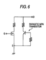
- the L-DMOSFET as shown in Fig. 6, is inevitably accompanied by a parasitic NPN transistor (having an NPN structure including a drain region 103, a body region 105 and the N+-type source region 106), however.
- This parasitic NPN transistor frequently hinders various normal operations of the L-DMOSFET.
- the L-DMOSFET When the L-DMOSFET is used in an open drain state, static electricity is applied to the output terminal (drain), the static electricity is trapped, and its entire current flows within the L-DMOSFET. At this time, the parasitic NPN transistor operates as in a positive feedback mode with respect to temperature. As a result, current concentrates at a weak part of the transistor, which was formed during its manufacturing process. And the device will easily be broken.
- IGBT insulated gate bipolar transistor
- the IGBT is attendant with a parasitic thyristor (an NPN transistor formed with a drain region 103, a body region 105 and an N+-type source region 106, and a PNP transistor formed with the body region 105, a drain region 103 and the P+-type drain contact region 110).
- a parasitic thyristor an NPN transistor formed with a drain region 103, a body region 105 and an N+-type source region 106
- a PNP transistor formed with the body region 105, a drain region 103 and the P+-type drain contact region 110.
- a conductivity of the drain region 103 is varied to reduce a resistance component by positive holes that are injected into the drain region 103 from the P+-type drain contact region 110, which is formed by diffusing a P-type impurity into the drain region (collector) 103. Accordingly, the IGBT is frequently used as a high voltage withstanding element of 100V or higher and having a relatively long drift length (d).
- the IGBT is a punch-through device. Accordingly, it is impossible to set the drift length to be too long. Accordingly, it is rare that the IGBT is used in a relatively low voltage region of 100V or lower. There is no merit to integrate the IGBTs into an IC when comparing with the L-DMOSFET. Therefore, the use of the IGBT is vanishigly improbable.
- a loss of the Vf (forward voltage) value of the IGBT is large at an initial stage of its start. Therefore, in a low current region, the on-resistance of the IGBT is higher than that of the L-DMOSFET, and the IGBT has many disadvantages. Further, in a large current region, the latch-up of the parasitic thyristor is easy to occur. Accordingly, care must be taken for use conditions. Further, minority carriers take part in the operation of the IGBT. Accordingly, the frequency characteristic of the IGBT is inferior to that of the L-DMOSFET. This also is recognized as a large defect of the IGBT.
- the conventional L-DMOSFET is advantageous in that it is easy to attain a high voltage standing performance and is low in on-resistance, but is disadvantageous in that the Electro-Static discharge performance (ESD) is low.
- the IGBT is advantageous in that its Electrostatic discharge performance (ESD) is extremely high, but has many disadvantages: For example, it is not suitable for high integration; the on-resistance is high in a low current region; and the frequency characteristic is bad.
- an object of the invention is to provided an L-DMOSFET which has a high Electro-Static discharge performance (ESD) without any degradation of the characteristics proper to the L-DMOSFET and any increase of the element area, and a semiconductor device using the same.
- ESD Electro-Static discharge performance
- a double diffusion MOSFET comprising: a drain region of an N-type semiconductor layer formed on a semiconductor substrate; a body region of a P-type semiconductor region formed in the drain region; an N-type source region formed in the body region; and a gate electrode formed on a surface of the body region with a g ate insulating film being interposed therebetween, wherein the drain region contains N+ type drain contact regions formed on a surface of the drain region and P+ type regions electrically connected to the N+ type drain contact regions so that the N+ type drain contact regions and the P+ type regions are put at an equal potential.
- the N+ type drain contact regions and the P+ type regions are formed in the drain region, while being at an equal potential, whereby a PNP transistor is parasitic to the L-MOSFET.
- This parasitic PNP transistor and the originally present NPN transistor cooperatively form a parasitic thyristor.
- the N+ type drain contact regions and the P+ type regions are put at an equal potential. Accordingly, in a normal operation of the L-DMOSFET, the parasitic thyristor may be prohibited from being turned on.
- the drain region formed so as to come in contact with the N+ type drain contact regions extends to a surface of the P-type regions.
- the N+ type drain contact regions and the P+ type regions are in electrical contact with one another.
- the N+ type drain contact regions are brought into electrical contact with the P+ type regions by the drain electrode. Therefore, those regions may easily be put at the equal potential by only the drawing of the electrode.
- the N+ type drain contact regions are shaped like a comb, and the P+ type regions are each placed in a gaps each between the adjacent projections thereof.
- the N+ type drain contact region is cut out at plural positions, equidistantly spaced, along the N-type source region.
- the P+ type regions are provided at each of those cutout parts.
- the N+ type drain contact regions are shaped like a comb of which the projections are located on the gate side, and the P+ type regions are each placed in a gaps each between the adjacent projections thereof.
- the P+ type regions are provided within the N+ type drain contact regions, whereby a parasitic thyristor may easily be formed.
- An end of the P+ type region closer to the body region is preferably separated (set back) further apart from the body region than an end of the N+ type drain contact region closer to the region.
- the L-DMOSFET of the invention is capable of greatly improving the Electro-Static discharge performance (ESD) without any increase of the element area, while retaining the characteristics of the conventional L-DMOSFET.
- ESD Electro-Static discharge performance
- the P+ type regions are formed in an area surrounded by the N+ type drain contact regions.
- the L-DMOSFET of the invention is capable of greatly improving the Electro-Static discharge performance (ESD) without any increase of the element area, while retaining the characteristics of the conventional L-DMOSFET.
- ESD Electro-Static discharge performance
- the P+ type regions and the N+ type drain contact regions are preferably formed in an N buffer layer formed in the drain region.
- This feature further improves the punch through breakdown voltage and farther reduces the on-resistance.
- a semiconductor device of the invention is formed by integrating the L-DMOSFET of the invention together with another element.
- a semiconductor device comprises: a semiconductor substrate; a drain region of an N-type semiconductor region formed on a surface of the semiconductor substrate; a body region of a P-type secured with the drift length equal to that of the conventional L-DMOSFET.
- the L-DMOSFET of the invention is capable of greatly improving the Electro-Static discharge performance (ESD) without any increase of the element area, while retaining the characteristics of the conventional L-DMOSFET.
- the P+ type regions are formed in an area surrounded by the N+ type drain contact regions.
- the L-DMOSFET of the invention is capable of greatly improving the Electro-Static discharge performance (ESD) without any increase of the element area, while retaining the characteristics of the conventional L-DMOSFET.
- ESD Electro-Static discharge performance
- the P+ type regions and the N+ type drain contact regions are preferably formed in an N buffer layer formed in the drain region.
- This feature further improves the punch through breakdown voltage and further reduces the on-resistance.
- a semiconductor device of the invention is formed by integrating the L-DMOSFET of the invention together with another element.
- a semiconductor device comprises: a semiconductor substrate; a drain region of an N-type semiconductor region formed on a surface of the semiconductor substrate; a body region of a P-type semiconductor region formed in the drain region; an N-type source region formed in the body region; a gate electrode formed on the body region with an gate insulating film being interposed therebetween; a gate electrode formed on a surface of the body region with a gate insulating film being interposed therebetween; N+ type drain contact regions formed on a surface of the drain region and P+ type regions electrically connected to the N+ type drain contact regions so that the N+ type drain contact regions and the P+ type regions are put at an equal potential, the N+ type drain contact regions and the P+ type regions being located within the drain region; a drain electrode extending from the N+ type drain contact regions to a surface of the P-type region; and a source electrode formed so as to come in contact with the N-type source region.
- the source electrode is formed extending to a surface of the P-type body region.
- the breakdown withstand voltage of the L-DMOSFET may easily be adjusted by varying the drift length of the L-DMOSFET to be integrated together with the element and the setback length of the P+ type region. Accordingly, the L-DMOSFET 10 may be used as a protection element in connection with the withstand voltage of the element 26.
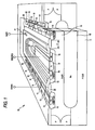
- Fig. 1 is a cross sectional view perspectively showing a double diffusion MOSFET which is an embodiment of the invention.
- a drain region 13 is formed in a manner that an N-type semiconductor layer is epitaxially grown on a P-type semiconductor substrate 11 with an N+ type buried region 12 being interposed therebetween.
- An N + buffer layer 14 is formed by diffusing an N-type impurity into the drain region 13.
- a body region 15 is formed by diffusing a P-type imipurity into the same.
- N + -type source region 16 is formed in a surface region of the body region 15, while being spaced apart from an outer edge of the body region 15.
- a P+-type region 17 is formed on the inner side of the N+-type region 16.
- N+ type drain contact regions 18 and P+ type regions 19,while being in contact with one another are alternately arrayed along the N+ type source region 16.
- a drift channel region 20 is formed between the N+ type source region 16 and the N+ buffer layer 14.
- a gate electrode is provided covering a surface region ranging from an outer edge part of the N+-type source region 16 to the inner edge part of the drift channel region 20, while a gate oxide film is interposed therebetween.
- a drain electrode 22 so formed as to come in contact with an N+ type drain contact region 18 is formed so that a potential of the N+ type drain contact region 18 is equal to that of the P+ type region 19.
- a source electrode 23 is formed extending to both the N+ type source region 16 and the P+ type region 17.
- the N+ type drain contact region 18 is cut out at plural locations, equidistantly spaced, along the N-type source region.
- the P+ type region 19 is provided at each of those cutout parts.
- Each P+ type region 19 is disposed such that an end of the P+ type region closer to the body region 15 is set back from an end of the N+ type drain contact region 18 closer to the body region 15 by a distance of 1.0 ⁇ m, for example.
- the N+ type drain contact regions 18 and the P+ type regions 19, while being in contact with one another, are formed in the drain region 13, whereby a PNP transistor is parasitic to the L-MOSFET 10.
- This parasitic PNP transistor and the originally present NPN transistor cooperatively form a parasitic thyristor.
- the P+ type region 19 is laid out such that it is set back further from the body region 15 than the N+ type drain contact region 18 to thereby increase a withstand capability for a punch-through breakdown which occurs when a depletion layer extending between the source and the drain reaches the lateral double diffusion MOSFET 10 located closer to the drain.
- N+ type drain contact regions 18 and the P+ type regions 19 are covered with the N+ buffer layer 14
- a depletion layer extending toward the drain is gradually held back.
- the withstand capability of the P+ type region 19 for the punch-through breakdown is further improved.
- the N+ type drain contact region 18 located closer to the drain is cut out at spatial intervals to have a comb-like structure. As a result, its conduction capability is lowered.
- such a structure that the N+ type drain contact regions 18 are covered with the N+ buffer layer 14 completely compensates for the lowering of the conduction capability.
- FIG. 2 An equivalent circuit of this L-DMOSFET is shown in Fig. 2. As shown, the emitter and the base of the PNP transistor forming the parasitic thyristor of the L-DMOSFET are shortcircuited. Accordingly, normally the FET does not operate. Accordingly, the L-MOSFET 10, when turned on, operates like the conventional L-DMOSFET. Even in a large current region, no care must be taken to the presence of the parasitic thyristor. For the same reason, the L-DMOSFET is free from the Vf loss at its start time which essentially occurs in the IGBT, and secures a low on-resistance even in a low current region.
- the drain electrode 22 is extended to the surface of the N+ buffer layer 14, the P+ type regions 19 and the drain region 13 are put at an equal potential. Accordingly, injection of positive holes from the P+ type region 19 does not occur, while it occurs in the IGBT. Accordingly, a switching speed (frequency characteristic) of the L-DMOSFET 10 is comparable with that of the conventional L-DMOSFET.
- the PNP transistor If once a static electricity is applied to the L-DMOSFET, the PNP transistor is forcibly broken down by its high voltage, and the parasitic thyristor starts to operate. Accordingly, it can process considerably large current at considerably low on-resistance, so that the Electro-Static discharge performance (ESD) is remarkably improved.
- ESD Electro-Static discharge performance
- the L-DMOSFET 10 of the embodiment succeeds in increasing the Electro-Static discharge performance (ESD) to be 3 to 10 times as large as that of the conventional L-DMOSFET, by not using any new fabricating technique and without damaging the characteristic of the conventional L-DMOSFET.
- the Electro-Static discharge performance (ESD) of the conventional L-DMOSFET is about 1.5kV when measured by using a human body model.
- the Electro-Static discharge performance (ESD) of the L-DMOSFET of the invention was 4.5kV to 15kV, i.e., 3 to 10 times as large as that of the conventional L-DMOSFET.
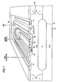
- Fig. 3 is a cross sectional view perspectively showing an L-MOSFET which is another embodiment of the invention.
- the instant embodiment employs a structure that the N+ type drain contact region 18 is bored at positions equidistantly spaced, instead of the structure that the N+ type drain contact region 18 located doser to the drain is cut out at positions spaced at spatial intervals.
- the P+ type regions 19 are buried in those bored parts, respectively, whereby the P+ type regions 19 are formed in an area surrounded by the N+ type drain contact region 18.
- the L-DMOSFET having a structure of Fig. 3 produces advantages comparable with those of the L-DMOSFET of the Fig. 1 embodiment.
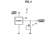
- Fig. 4 is a circuit diagram showing an electrical arrangement of a semiconductor device according to the invention.
- This semiconductor device 25 is manufactured by integrating L-DMOSFET 10 thus structured together with another element 26.
- the breakdown withstand voltage of the L-DMOSFET 10 may easily be adjusted by varying the drift length "d" of the L-DMOSFET 10 to be integrated together with the element 26 and the setback length of the P+ type region 19. Accordingly, the L-DMOSFET 10 may be used as a protection element in connection with the withstand voltage of the element 26.
- the N+ type drain contact regions and P+ type regions are formed in the drain region such that those regions are put at an equal potential. Accordingly, the MOSFET is attendant with a parasitic thyristor. There is no need of lowering a gain of the parasitic NPN transistor, and hence there is no chance of degrading the characteristic proper o the L-DMOSFET. Further, there is no need of using a protection circuit to improve the breakdown resistance quantity, and hence, a high Electrostatic discharge performance (ESD) is secured without increasing the element area.
- ESD Electrostatic discharge performance
- Electro-Static discharge performance is secured when a lateral double diffusion MOSFET is used as a protection element for an internal circuit (or internal element).
- a double diffusion MOSPET which comprises: a drain region 13 of an N-type semiconductor layer formed on a semiconductor substrate 11; a body region 15 of a P-type semiconductor region formed in the drain region 13; an N-type source region 16 formed in the body region 15; and a gate electrode 21 formed on a surface of the body region 15, wherein the drain region 13 contains N+ type drain contact regions 18 and P+ type regions 19 such that those are put at an equal potential.
Landscapes
- Insulated Gate Type Field-Effect Transistor (AREA)
Abstract
Description
Claims (8)
- A double diffusion MOSFET comprising:wherein said drain region contains N+ type drain contact regions formed on a surface of said drain region and P+ type regions electrically connected to said N+ type drain contact regions so that said N+ type drain contact regions and said P+ type regions are put at an equal potential.a drain region of an N-type semiconductor layer formed on a semiconductor substrate;a body region of a P-type semiconductor region formed in said drain region;an N-type source region formed in said body region; anda gate electrode formed on a surface of said body region with a gate insulating film being interposed therebetween,
- A double diffusion MOSFET according to claim 1, wherein said drain region formed so as to come in contact with said N+ type drain contact regions extends to a surface of said P-type regions.
- A double diffusion MOSFET according to claim 1 or 2, wherein said N+ type drain contact regions are shaped like a comb, and said P+ type regions are each placed in a gaps each between the adjacent projections thereof.
- A double diffusion MOSFET according to claim 1 or 2, wherein said N+ type drain contact regions are shaped like a comb of which the projections are located on the gate side, and said P+ type regions are each placed in a gaps each between the adjacent projections thereof.
- A double diffusion MOSFET according to any of claims 1 to 3, wherein an end of said P+ type region closer to said body region is set back further from said body region than an end of said N+ type drain contact region closer to said region.
- A double diffusion MOSFET according to claim 1 or 2, wherein said P+ type regions are formed in an area surrounded by said N+ type drain contact regions.
- A double diffusion MOSFET according to any of claims 1 to 6, wherein said P+ type regions and said N+ type drain contact regions are formed in an N buffer layer formed in said drain region.
- A semiconductor device comprising:a semiconductor substrate;a drain region of an N-type semiconductor region formed on a surface of said semiconductor substrate;a body region of a P-type semiconductor region formed in said drain region; an N-type source region formed in said body region;a gate electrode formed on said body region with an gate insulating film being interposed therebetween;a gate electrode formed on a surface of said body region with a gate insulating film being interposed therebetween,N+ type drain contact regions formed on a surface of said drain region and P+ type regions electrically connected to said N+ type drain contact regions so that said N+ type drain contact regions and said P+ type regions are put at an equal potential, said N+ type drain contact regions and said P+ type regions being located within said drain region;a drain electrode extending from said N+ type drain contact regions to a surface of said P-type region; anda source electrode formed so as to come in contact with said N-type source region.
Applications Claiming Priority (2)
| Application Number | Priority Date | Filing Date | Title |
|---|---|---|---|
| JP2002010127A JP3824310B2 (en) | 2002-01-18 | 2002-01-18 | Double diffusion MOSFET and semiconductor device using the same |
| JP2002010127 | 2002-01-18 |
Publications (3)
| Publication Number | Publication Date |
|---|---|
| EP1331672A2 true EP1331672A2 (en) | 2003-07-30 |
| EP1331672A3 EP1331672A3 (en) | 2004-10-27 |
| EP1331672B1 EP1331672B1 (en) | 2008-03-26 |
Family
ID=19191571
Family Applications (1)
| Application Number | Title | Priority Date | Filing Date |
|---|---|---|---|
| EP03001022A Expired - Lifetime EP1331672B1 (en) | 2002-01-18 | 2003-01-17 | Double diffusion MOSFET |
Country Status (5)
| Country | Link |
|---|---|
| US (1) | US6914298B1 (en) |
| EP (1) | EP1331672B1 (en) |
| JP (1) | JP3824310B2 (en) |
| CN (1) | CN100349302C (en) |
| DE (1) | DE60319899T2 (en) |
Families Citing this family (29)
| Publication number | Priority date | Publication date | Assignee | Title |
|---|---|---|---|---|
| US7098509B2 (en) * | 2004-01-02 | 2006-08-29 | Semiconductor Components Industries, L.L.C. | High energy ESD structure and method |
| JP4197660B2 (en) | 2004-04-30 | 2008-12-17 | ローム株式会社 | MOS transistor and semiconductor integrated circuit device having the same |
| JP2006054247A (en) * | 2004-08-10 | 2006-02-23 | Fuji Electric Device Technology Co Ltd | Semiconductor device |
| US7759696B2 (en) | 2005-10-20 | 2010-07-20 | Panasonic Corporation | High-breakdown voltage semiconductor switching device and switched mode power supply apparatus using the same |
| JP4695961B2 (en) * | 2005-10-20 | 2011-06-08 | パナソニック株式会社 | High voltage semiconductor switching element and switching power supply device using the same |
| DE102005060521A1 (en) * | 2005-12-09 | 2007-06-14 | Atmel Germany Gmbh | DMOS transistor with optimized edge structure |
| JP4630207B2 (en) * | 2006-03-15 | 2011-02-09 | シャープ株式会社 | Semiconductor device |
| JP2007318062A (en) * | 2006-04-27 | 2007-12-06 | Matsushita Electric Ind Co Ltd | High voltage semiconductor switching element |
| JP5431663B2 (en) * | 2006-09-15 | 2014-03-05 | セミコンダクター・コンポーネンツ・インダストリーズ・リミテッド・ライアビリティ・カンパニー | Semiconductor device and manufacturing method thereof |
| US7531888B2 (en) * | 2006-11-30 | 2009-05-12 | Fairchild Semiconductor Corporation | Integrated latch-up free insulated gate bipolar transistor |
| JP4788749B2 (en) * | 2007-11-09 | 2011-10-05 | 株式会社デンソー | Semiconductor device |
| JP5515248B2 (en) * | 2008-03-26 | 2014-06-11 | 富士電機株式会社 | Semiconductor device |
| JP5329118B2 (en) * | 2008-04-21 | 2013-10-30 | セミコンダクター・コンポーネンツ・インダストリーズ・リミテッド・ライアビリティ・カンパニー | DMOS transistor |
| CN101771077B (en) * | 2008-12-30 | 2015-01-07 | 世界先进积体电路股份有限公司 | Horizontal Diffused Metal Oxide Semiconductor Transistor Device with Electrostatic Discharge Protection |
| JP2010278258A (en) * | 2009-05-28 | 2010-12-09 | Panasonic Corp | High voltage semiconductor device and current control device using the same |
| JP2011018809A (en) * | 2009-07-09 | 2011-01-27 | Panasonic Corp | Semiconductor device and method of manufacturing the same |
| US8120108B2 (en) * | 2010-01-27 | 2012-02-21 | Texas Instruments Incorporated | High voltage SCRMOS in BiCMOS process technologies |
| US8125030B2 (en) * | 2010-01-27 | 2012-02-28 | Texas Instruments Incorporated | High voltage SCRMOS in BiCMOS process technologies |
| US20130087828A1 (en) * | 2010-06-21 | 2013-04-11 | Renesas Electronics Corporation | Semiconductor device and method for manufacturing same |
| CN104115275B (en) * | 2012-02-16 | 2017-02-15 | 瑞萨电子株式会社 | Semiconductor device |
| CN103839998B (en) * | 2012-11-27 | 2017-10-24 | 上海华虹宏力半导体制造有限公司 | LDMOS device and its manufacture method |
| US9337178B2 (en) * | 2012-12-09 | 2016-05-10 | Semiconductor Components Industries, Llc | Method of forming an ESD device and structure therefor |
| JP6255421B2 (en) * | 2013-01-30 | 2017-12-27 | マイクロチップ テクノロジー インコーポレイテッドMicrochip Technology Incorporated | DMOS semiconductor device having ESD self-protection and LIN bus driver having the same |
| CN106206561B (en) * | 2015-04-29 | 2019-05-10 | 无锡华润上华科技有限公司 | Electrostatic protection device of LDMOS thyristor structure |
| CN104992977B (en) | 2015-05-25 | 2018-06-19 | 上海华虹宏力半导体制造有限公司 | NLDMOS device and its manufacturing method |
| US10249614B2 (en) | 2015-05-28 | 2019-04-02 | Macronix International Co., Ltd. | Semiconductor device |
| US10217733B2 (en) | 2015-09-15 | 2019-02-26 | Semiconductor Components Industries, Llc | Fast SCR structure for ESD protection |
| JP7279393B2 (en) * | 2019-02-15 | 2023-05-23 | 富士電機株式会社 | Manufacturing method of semiconductor integrated circuit |
| CN114556560B (en) | 2019-11-29 | 2026-01-23 | 罗姆股份有限公司 | Semiconductor device with a semiconductor layer having a plurality of semiconductor layers |
Family Cites Families (4)
| Publication number | Priority date | Publication date | Assignee | Title |
|---|---|---|---|---|
| US5168333A (en) | 1987-02-26 | 1992-12-01 | Kabushiki Kaisha Toshiba | Conductivity-modulation metal oxide semiconductor field effect transistor |
| EP0361589B1 (en) * | 1988-09-22 | 2001-12-19 | Koninklijke Philips Electronics N.V. | Segmented-anode lateral insulated-gate bipolar transistor devices |
| US5155562A (en) * | 1990-02-14 | 1992-10-13 | Fuji Electric Co., Ltd. | Semiconductor device equipped with a conductivity modulation misfet |
| JP4357127B2 (en) | 2000-03-03 | 2009-11-04 | 株式会社東芝 | Semiconductor device |
-
2002
- 2002-01-18 JP JP2002010127A patent/JP3824310B2/en not_active Expired - Lifetime
-
2003
- 2003-01-16 CN CNB031015212A patent/CN100349302C/en not_active Expired - Lifetime
- 2003-01-17 DE DE60319899T patent/DE60319899T2/en not_active Expired - Lifetime
- 2003-01-17 US US10/346,806 patent/US6914298B1/en not_active Expired - Lifetime
- 2003-01-17 EP EP03001022A patent/EP1331672B1/en not_active Expired - Lifetime
Also Published As
| Publication number | Publication date |
|---|---|
| JP3824310B2 (en) | 2006-09-20 |
| DE60319899T2 (en) | 2009-04-09 |
| EP1331672B1 (en) | 2008-03-26 |
| JP2003218348A (en) | 2003-07-31 |
| EP1331672A3 (en) | 2004-10-27 |
| US6914298B1 (en) | 2005-07-05 |
| CN1433083A (en) | 2003-07-30 |
| CN100349302C (en) | 2007-11-14 |
| DE60319899D1 (en) | 2008-05-08 |
Similar Documents
| Publication | Publication Date | Title |
|---|---|---|
| US6914298B1 (en) | Double diffusion MOSFET with N+ and P+ type regions at an equal potential | |
| US8802509B2 (en) | Configuration of gate to drain (GD) clamp and ESD protection circuit for power device breakdown protection | |
| US8482031B2 (en) | Lateral insulated gate bipolar transistors (LIGBTS) | |
| US6713794B2 (en) | Lateral semiconductor device | |
| JP4129306B2 (en) | Vertical semiconductor device controllable by field effect and manufacturing method thereof | |
| US6809349B2 (en) | Power semiconductor device | |
| EP1187214B1 (en) | Semiconductor device with a protection against ESD | |
| US5698454A (en) | Method of making a reverse blocking IGBT | |
| US6864533B2 (en) | MOS field effect transistor with reduced on-resistance | |
| JP2942732B2 (en) | Shorted anode horizontal insulated gate bipolar transistor | |
| US5631483A (en) | Power device integrated structure with low saturation voltage | |
| JP2002261297A (en) | Lateral MOS field effect transistor having lightly doped drain and method of manufacturing the same | |
| KR20030005385A (en) | Field effect transistor structure and method of manufacture | |
| US11139292B2 (en) | Conductivity modulated drain extended MOSFET | |
| US9620498B2 (en) | Configuration of gate to drain (GD) clamp and ESD protection circuit for power device breakdown protection | |
| JPH10233508A (en) | DMOS transistor protected from "snap back" | |
| JP2680788B2 (en) | Integrated structure active clamp device | |
| US5757034A (en) | Emitter switched thyristor | |
| US8022506B2 (en) | SOI device with more immunity from substrate voltage | |
| EP0115098B1 (en) | Lateral dmos transistor device having an injector region | |
| CN115732553A (en) | IGBT device and preparation method thereof | |
| US5909039A (en) | Insulated gate bipolar transistor having a trench | |
| US11482615B2 (en) | Super-junction power MOSFET device with improved ruggedness, and method of manufacturing | |
| JP3522532B2 (en) | Semiconductor device | |
| EP1443649A1 (en) | Emitter switching configuration and corresponding integrated structure |
Legal Events
| Date | Code | Title | Description |
|---|---|---|---|
| PUAI | Public reference made under article 153(3) epc to a published international application that has entered the european phase |
Free format text: ORIGINAL CODE: 0009012 |
|
| AK | Designated contracting states |
Designated state(s): AT BE BG CH CY CZ DE DK EE ES FI FR GB GR HU IE IT LI LU MC NL PT SE SI SK TR |
|
| AX | Request for extension of the european patent |
Extension state: AL LT LV MK RO |
|
| PUAL | Search report despatched |
Free format text: ORIGINAL CODE: 0009013 |
|
| AK | Designated contracting states |
Kind code of ref document: A3 Designated state(s): AT BE BG CH CY CZ DE DK EE ES FI FR GB GR HU IE IT LI LU MC NL PT SE SI SK TR |
|
| AX | Request for extension of the european patent |
Extension state: AL LT LV MK RO |
|
| 17P | Request for examination filed |
Effective date: 20050125 |
|
| 17Q | First examination report despatched |
Effective date: 20050225 |
|
| AKX | Designation fees paid |
Designated state(s): DE FR IT NL |
|
| GRAP | Despatch of communication of intention to grant a patent |
Free format text: ORIGINAL CODE: EPIDOSNIGR1 |
|
| GRAS | Grant fee paid |
Free format text: ORIGINAL CODE: EPIDOSNIGR3 |
|
| GRAA | (expected) grant |
Free format text: ORIGINAL CODE: 0009210 |
|
| AK | Designated contracting states |
Kind code of ref document: B1 Designated state(s): DE FR IT NL |
|
| REF | Corresponds to: |
Ref document number: 60319899 Country of ref document: DE Date of ref document: 20080508 Kind code of ref document: P |
|
| ET | Fr: translation filed | ||
| PLBE | No opposition filed within time limit |
Free format text: ORIGINAL CODE: 0009261 |
|
| STAA | Information on the status of an ep patent application or granted ep patent |
Free format text: STATUS: NO OPPOSITION FILED WITHIN TIME LIMIT |
|
| 26N | No opposition filed |
Effective date: 20081230 |
|
| PGFP | Annual fee paid to national office [announced via postgrant information from national office to epo] |
Ref country code: FR Payment date: 20090127 Year of fee payment: 7 |
|
| REG | Reference to a national code |
Ref country code: FR Ref legal event code: ST Effective date: 20100930 |
|
| PG25 | Lapsed in a contracting state [announced via postgrant information from national office to epo] |
Ref country code: FR Free format text: LAPSE BECAUSE OF NON-PAYMENT OF DUE FEES Effective date: 20100201 |
|
| PGFP | Annual fee paid to national office [announced via postgrant information from national office to epo] |
Ref country code: DE Payment date: 20120111 Year of fee payment: 10 |
|
| PGFP | Annual fee paid to national office [announced via postgrant information from national office to epo] |
Ref country code: IT Payment date: 20120119 Year of fee payment: 10 |
|
| PGFP | Annual fee paid to national office [announced via postgrant information from national office to epo] |
Ref country code: NL Payment date: 20120125 Year of fee payment: 10 |
|
| REG | Reference to a national code |
Ref country code: NL Ref legal event code: V1 Effective date: 20130801 |
|
| PG25 | Lapsed in a contracting state [announced via postgrant information from national office to epo] |
Ref country code: NL Free format text: LAPSE BECAUSE OF NON-PAYMENT OF DUE FEES Effective date: 20130801 Ref country code: DE Free format text: LAPSE BECAUSE OF NON-PAYMENT OF DUE FEES Effective date: 20130801 |
|
| REG | Reference to a national code |
Ref country code: DE Ref legal event code: R119 Ref document number: 60319899 Country of ref document: DE Effective date: 20130801 |
|
| PG25 | Lapsed in a contracting state [announced via postgrant information from national office to epo] |
Ref country code: IT Free format text: LAPSE BECAUSE OF NON-PAYMENT OF DUE FEES Effective date: 20130117 |