EP1331669A2 - Antifuse structure and method of making - Google Patents
Antifuse structure and method of making Download PDFInfo
- Publication number
- EP1331669A2 EP1331669A2 EP02259033A EP02259033A EP1331669A2 EP 1331669 A2 EP1331669 A2 EP 1331669A2 EP 02259033 A EP02259033 A EP 02259033A EP 02259033 A EP02259033 A EP 02259033A EP 1331669 A2 EP1331669 A2 EP 1331669A2
- Authority
- EP
- European Patent Office
- Prior art keywords
- antifuse
- thermal conductivity
- forming
- control element
- thermal
- Prior art date
- Legal status (The legal status is an assumption and is not a legal conclusion. Google has not performed a legal analysis and makes no representation as to the accuracy of the status listed.)
- Withdrawn
Links
Images






Classifications
-
- H—ELECTRICITY
- H10—SEMICONDUCTOR DEVICES; ELECTRIC SOLID-STATE DEVICES NOT OTHERWISE PROVIDED FOR
- H10W—GENERIC PACKAGES, INTERCONNECTIONS, CONNECTORS OR OTHER CONSTRUCTIONAL DETAILS OF DEVICES COVERED BY CLASS H10
- H10W20/00—Interconnections in chips, wafers or substrates
- H10W20/40—Interconnections external to wafers or substrates, e.g. back-end-of-line [BEOL] metallisations or vias connecting to gate electrodes
- H10W20/49—Adaptable interconnections, e.g. fuses or antifuses
- H10W20/491—Antifuses, i.e. interconnections changeable from non-conductive to conductive
-
- Y—GENERAL TAGGING OF NEW TECHNOLOGICAL DEVELOPMENTS; GENERAL TAGGING OF CROSS-SECTIONAL TECHNOLOGIES SPANNING OVER SEVERAL SECTIONS OF THE IPC; TECHNICAL SUBJECTS COVERED BY FORMER USPC CROSS-REFERENCE ART COLLECTIONS [XRACs] AND DIGESTS
- Y10—TECHNICAL SUBJECTS COVERED BY FORMER USPC
- Y10S—TECHNICAL SUBJECTS COVERED BY FORMER USPC CROSS-REFERENCE ART COLLECTIONS [XRACs] AND DIGESTS
- Y10S438/00—Semiconductor device manufacturing: process
- Y10S438/957—Making metal-insulator-metal device
Definitions
- the present invention relates to antifuse structures, and is more particularly related to thermal isolation of antifuse structures and methods of making same.
- Antifuse structures include a material which initially has a high resistance but which can be converted into a low resistance material by the application of a programming voltage.
- the programming voltage is in excess of a breakdown voltage of the high resistance material.
- the high resistance material is an electrically insulating antifuse layer which is sandwiched between a pair of electrically conductive layers. Each electrically conductive layer in the pair is generally considered an electrode of the antifuse structure.
- the high resistance material also called an antifuse material, is non-conductive when manufactured but is caused to become permanently conductive by application of the programming voltage across the pair of electrically conductive layers.
- an electrically conductive filament forms in the antifuse layer.
- the newly formed electrically conductive filament in the antifuse layer which can be as narrow as several atoms in width, is effective as an electrical short of the two electrically conductive layers, thus programming the antifuse structure.
- Those antifuse structures that remain unprogrammed have no electrically conductive filament connecting their respective pair of electrically conductive layers.
- Antifuse structures can be used in certain classes of IC chips such as field programmable gate arrays (FPGAs), programmable read-only memories (PROMs) and the like.
- FPGAs typically include a large number of logic elements, such as AND gates and OR gates, which can be selectively coupled to perform user designed functions. Programming a FPGA is generally accomplished by applying a programming voltage to selected antifuse structures thereby converting them into conductive interconnections.
- an antifuse structure has an antifuse between first and second thermal conduction regions.
- Each of the first and second thermal conduction regions has a portion of low thermal conductivity and a portion of high thermal conductivity.
- the portion having low thermal conductivity is between the respective portion of high thermal conductivity and the antifuse.
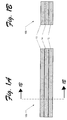
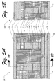
- a structure 100 includes an interlayer dielectric (ILD) 12.
- ILD 12 is preferably composed of an electrical insulator material that includes but is not limited to a wet or dry silicon dioxide (SiO 2 ), a nitride material including silicon nitride, tetraethylorthosilicate (Si-OC 2 H 5 ) 4 ) (TEOS) based oxides, borophosphosilicate glass (BPSG), phosphosilicate glass (PSG), borosilicate glass (BSG), oxide-nitride-oxide (ONO), polyamide film, tantalum pentoxide (Ta 2 O 5 ), plasma enhanced silicon nitride (P-SiN x ), titanium oxide, oxynitride, germanium oxide, a spin on glass (SOG), any chemical vapor deposited (
- An electrically conductive row line 14 is formed upon ILD 12.
- Row line 14 can be patterned so as to form a word line for memory cells, and will preferably have a thickness in a range from about 200 Angstroms to about 10,000 Angstroms, and most preferably about 1,800 Angstroms.
- the composition of row line 14 can be a metal such aluminum, copper, or an aluminum-copper alloy, and can also be composed of amorphous silicon or microcrystalline silicon.
- Electrically conductive silicides such as refractory metal silicides, are also contemplated as materials for row line 14.
- a thermal insulator 16 is formed upon row line 14. The thermal conductivity properties of the material of which thermal insulator 16 is composed will preferably be significantly lower than that of row line 14.
- the thermal properties of a material are typically measured as thermal conductivity in the SI units of watts per meter Kelvin (W/mK) or Joules/Second-Meter-Degrees Centigrade.
- alumina has a thermal conductivity of about 17 Joules/Second-Meter-Degrees Centigrade and aluminum has a thermal conductivity of about 234 Joules/Second-Meter-Degrees Centigrade.
- the thermally insulative materials disclosed herein, for thermally isolating embodiments of the thermally isolated antifuse structure will have thermal conductivities lesser by at least an order of magnitude than that of the highly thermally conductive structures associated with the antifuse structure.
- Antifuse structures can thus be thermally isolated by the thermally insulative materials disclosed herein (i) around the periphery of the electrodes, (ii) above and below the electrodes, (iii) both around the periphery and above and below the electrodes, and (iv) by the electrode material thermal properties.
- the thermal conductivity of the electrodes of the antifuse structure will preferably be in a range of metals from about 10 W/mK to about 100 W/mK, and the material for thermally insulating the electrodes will have a thermal conductivity preferably be in a range of oxides/gases from about zero (0) W/mK to about 25 W/mK.
- Thermal insulator 16 which can be an oxide or a ceramic such as alumina (e.g. Al 2 O 3 ), will preferably be deposited in a thickness in a range from about 200 Angstroms to about 1000 Angstroms, and most preferably about 600 Angstroms.
- thermal insulator 16 can be composed of alumina (e.g. Al 2 O 3 ).
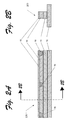
- FIGS 2A-2B show a structure 200 that is the result of further and conventional processing operations upon structure 100 seen in Figures 1A-1B.
- Structure 200 depicts thermal insulator 16 as being planarized, such as by conventional processing. Following the planarization of thermal insulator 16, via plugs 18 are formed through thermal insulator 16 for row line 14. Via plugs 18 and thermal insulator 16 may then be planarized.
- a thin electrode 15 is formed upon the planarized surface of via plugs 18 and thermal insulator 16. Thin electrode 15 will preferably have a thickness in a range from about 50 Angstroms to about 1000 Angstroms, and most preferably about 200 Angstroms.
- the composition of thin electrode 15, which is electrically conductive can be composed of a metal such as titanium with a low thermal conductivity or with metals with higher thermal conductivities such as aluminum, copper, or an aluminum-copper alloy.
- Amorphous silicon, microcrystalline silicon, or polysilicon can also be the composition of thin electrode 15.
- Thin electrode 15, which is patterned to form the base of the structure 200, will preferably have a significantly smaller cross sectional area as compared to row line 14, to further limit thermal conduction away from the structure 200.
- Each via plug 18 is formed by conventional processing and will preferably be electrically conductive and capable of withstanding the intended current density of adjacent antifuse structures.
- Each of the via plugs 18 will preferably have a low thermal conductivity and can be composed of electrically conductive refractory metals and their alloys and nitrides, such as tungsten, tungsten silicide, and tungsten nitride.
- the material used for form via plugs 18 can contribute to a higher thermal barrier for thermal isolation of antifuse structures during the programming process.
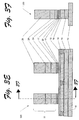
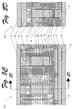
- FIG. 3A-3B Three different embodiments of the invention are set forth, respectively, in Figures 3A-3B, in Figures 3C-3D, and in Figures 3E-3F.
- Each of these three different embodiments depict a structure 300 that is the result of conventional processing upon structure 200 seen in Figures 2A-2B to form an antifuse layer 20 and a control element 22 over thin electrode 15.
- Figures 3A-3B show control element 22 upon antifuse layer 20, where antifuse layer 20 is upon thin electrode 15.
- Figures 3C-3D show control element 22 upon a thin electrode 17, where thin electrode 17 is upon antifuse layer 20.
- Figures 3E-3F show control element 22 over antifuse layer 20, where antifuse layer 20 is sandwiched between a pair of thin electrodes 17, and where the lowest thin electrode 17 is situated upon thin electrode 15. It is preferred that thin electrode 17 be thicker than thin electrode 15. Thin electrode 17 can be, but need not be, thicker than the row line 14.
- control element 22 is a diode.
- the diode can include N-type, P-type, and intrinsic or undoped regions.
- control element 22 is a tunnel junction.
- the tunnel junction can be an electrical insulator sandwiched between electrically conductive electrodes.
- Conventional processes are used to form antifuse layer 20, such as by oxide deposition.
- Antifuse layer 20, which will preferably have a thickness in a range from about 15 Angstroms to about 300 Angstroms, and most preferably about 50 Angstroms, is composed of a high resistance material that can be converted into a low resistance material by the application of a programming voltage that induces a state change in antifuse layer 20.
- Antifuse layer 20 is an electrical insulator. In use, antifuse layer 20 is made to be permanently conductive by application of the programming voltage across thin electrode 15 and control element 22. When thin electrode 15 is aluminum, antifuse layer 20 can be alumina (e.g. Al 2 O 3 ), such as by a patterning and an oxidation of the depicted portion of thin electrode 15.
- alumina e.g. Al 2 O 3
- Thermal insulator 16, thin electrodes 15 and 17, and via plugs 18 are sufficiently low in thermal conduction so as to provide thermal isolation during the process of heating up antifuse layer 20 and the interface of antifuse layer 20 to control element 22 and thin electrode 15 when an electrically conductive filament is formed in an antifuse layer 20 by application of the programming voltage.
- thermal insulator 16, thin electrodes 15 and 17, and via plugs 18 function to hold or retain heat in the antifuse structure. Less current for a shorter time is thereby required to be supplied to the antifuse layer during programming, and less power is used during programming of the antifuse structure.
- the device in which the thermally isolated antifuse structures are located will have a faster write speed in programming and will use less power.
- a lower power requirement permits a designer to use smaller, lower cost conductor layers and circuits in the memory device.
- the vertical stacks projecting from thin electrode 15 seen in Figures 3A-3F will use less power and current density due to the built-in thermal isolation so that these vertical stacks can also be smaller. The miniaturization of these vertical stacks further the industry-wide goal of higher scale integration on semiconductor die.
- control element 22 When control element 22 is a diode, the diode will preferably be composed of a semiconductor material having a p-doped region 24, an intrinsic or undoped region 26, and an n-doped region 28.
- the semiconductor material will preferably be deposited in a single deposition operation with altering or ramped dopants introduced during the deposition.
- the semiconductor material can be silicon, such as amorphous silicon or microcrystalline silicon. Alternatively, laser recrystallization can be used to form polysilicon in the making of the diode version of control element 22 from an initial deposition of amorphous silicon.
- control element 22 When control element 22 is a tunnel junction, the tunnel junction will include an electrical insulator 26 sandwiched between electrically conductive electrodes 24, 28.
- Control element 22 will have a preferred thickness in a range from about 800 Angstroms to about 1200 Angstroms, and most preferably about 1000 Angstroms. Control element 22 can function as a steering element in a memory cell to ascertain the state of the memory cell. Antifuse layer 20 can be used as a memory element to store a programmed state in the memory cell.
- Each vertical stack projecting from a respective segment of thin electrode 15 seen in Figures 3A-3F can be formed by several depositions of respective materials of the vertical stacks, followed by an anisotropic etch process of one or more etch recipes so as to form the depicted vertical stacks.
- etch recipes so as to form the depicted vertical stacks.
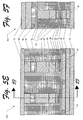
- an antifuse structure 400 seen in Figures 4A-4F results.
- An electrically insulative fill 30 is formed upon thin electrode 15 between each vertical stack projecting from thin electrode 15, where each vertical stack includes control element 22 and antifuse layer 20.
- Fill 30 can be composed of any of the materials that ILD 12 can be composed of.
- the thermal insulation properties of the material of which fill 30 is composed will preferably have a thermal conductivity much lower, and most preferably of at least an order of magnitude, than that of the memory cell structures that are in contact therewith (e.g. thin electrode 15 and control element 22).
- fill 30 can be deposited using a TEOS precursor.
- the materials to form another thin electrode 15 and another electrical insulator 16 are formed upon control element 22 and fill 30.
- Via plugs 18 are formed within openings of the higher thermal insulator 16 according to the patterning thereof down to the higher thin electrodes 15.
- Via plugs 18 and thermal insulator 16 may then be planarized.
- Materials for a column line 32 can then be formed upon the optionally planarized top surface of via plugs 18 and thermal insulator 16.
- Fill 30 will preferably have a lower thermal conductivity than that of either row line 14 or column line 32.
- the column line 32 can then be patterned.
- Fill 30 will preferably electrically and thermally insulate the periphery of the vertical stacks as seen in structure 400 of Figures 4A-4F.
- thin electrode 15 be thinner than both the row line 14 and column line 32.
- thin electrode 17 be thicker than thin electrode 15 and can, but need not be, thicker than either row line 14 or the column line 32.
- ILD 12 is formed upon a preferably planar surface upon fill 30 and patterned column line 32 seen in structure 500 of Figures 5A-5F.
- the electrical insulator 16 over control element 22 will preferably be composed of the same material as the thermal insulator 16 below control element 22. If present, the material of which the higher thermal insulator 16 is composed will have thermal insulation properties higher than that of a column line 32.
- Column line 32 is electrically conductive, will be a bit line for a memory cell, and will preferably be composed of the same material and have the same thickness as row line 14.
- a plurality of antifuse structures such as structure 500 seen in Figures 5A-5F, are stacked one upon the other and are each separated by an interlayer dielectric so as to form a plurality of stacked memory cells in a three-dimensional memory structure.
- a plurality of row lines 14 and column lines 32 may be used to make up a three-dimensional memory structure having a plurality of memory cells.
- the stack seen in Figures 5A-5F from row line 14 through column line 32 would be repeated in many vertical sequences each being upon the overlying ILD 12 above fill 30.
- a plurality of these vertical sequences is contemplated to make a three-dimensional memory structure.
- the memory structure 500 can be characterized as a 2N architecture in that row and column lines are not shared by vertically adjacent memory cells. Rather, vertically adjacent memory cells are physically separated and electrically insulated one from another.
- Memory structure 500 can be made in number of ways.
- a memory cell is formed on an interlayer dielectric that is on a substrate.
- the memory cell is formed by forming a patterned row line over the substrate.
- An electrical insulator is formed upon the patterned row, where the electrical insulator has a plurality of via plugs therein that are in electrical communication with the patterned row line.
- a first electrode is formed upon the electrical insulator and also upon the via plugs that are in the electrical insulator.
- a plurality of patterned stacks is formed upon the first electrode. Each patterned stack includes an antifuse layer and a control element.
- a dielectric fill is formed upon the first electrode so as to interface the plurality of patterned stacks.
- a second electrode is formed upon the patterned stacks and upon the dielectric fill.
- a second electrical insulator is formed upon the second electrode.
- the second insulator has a plurality of via plugs therein.
- a patterned column line is formed upon the second electrical insulator and the via plugs therein.
- a plurality of the memory cells can each be vertically offset one from another by an interlayer dielectric. It is preferable that the row line and the column line each comprise aluminum or an alloy thereof, the via plugs each comprise refractory metal or alloy thereof, the dielectric fill comprises silicon dioxide, at least a portion of the control element comprises lightly doped amorphous or microcrystalline silicon, and that the antifuse layer comprises alumina.
- the control element is formed as a diode. In another embodiment of the invention, the control element is formed as a tunnel junction.
- Each of three different embodiments of the invention features an antifuse between first and second thermal conduction regions.
- Each of the first and second thermal conduction regions has a portion of low thermal conductivity and a portion of high thermal conductivity. It is preferable that the portion having low thermal conductivity has a thermal conductivity less by about an order of magnitude than that of the portion of high thermal conductivity.
- the portion having the low thermal conductivity is between the respective portion of high thermal conductivity and the antifuse.
- the antifuse is in antifuse layer 20 and the portion having the high thermal conductivity is made up of either row line 14 or column line 32.
- the portion having the low thermal conductivity is made up of thin electrode 15, thermal insulator 16, thin electrode 17, and via plugs 18, although Figures 5A-5B do not have thin electrode 17.
- antifuse layer 20 is between the first and second thermal conduction regions.
- the first thermal conduction region is made up of structures seen at reference numerals 14, 16, 18, and 15, and the second thermal conduction region is made up of structures seen at reference numerals 15, 18, 16, and 32, where control element 22 is between antifuse layer 20 and thin electrode 15.
- the second thermal conduction region is upon antifuse layer 20.
- Control element 22 upon antifuse layer 20 and antifuse layer 20 is upon thin electrode 15.
- antifuse layer 20 is between first and second thermal conduction regions.
- the first thermal conductive region is made up of structures seen at reference numerals 14, 16, 18, and 15, and the second thermal conduction region is made up of structures seen at reference numerals 17, 15, 18, 16, and 32, where control element 22 is between the pair of thin electrodes 17, 15, and where second thermal conduction region is upon the antifuse layer 20.
- Control element 22 upon a thin electrode 17 and thin electrode 17 is upon antifuse layer 20.
- antifuse layer 20 is between first and second thermal conduction regions and also between a pair of thin electrodes 17.
- the first thermal conductive region is made up of structures seen at reference numerals 14, 16, 18, 15, and 17, and the second thermal conduction region is made up of structures seen at reference numerals 17, 15, 18, 16, and 32.
- Control element 22 is between the pair of thin electrodes 17, 15, and the second thermal conduction region is upon the antifuse layer 20.
- Control element 22 is over antifuse layer 20, where antifuse layer 20 is sandwiched between a pair of thin electrodes 17, and where the lowest thin electrode 17 is situated upon thin electrode 15.
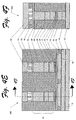
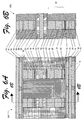
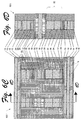
- FIG. 6A-6B Examples of three different embodiments of the invention are set forth, respectively, in Figures 6A-6B, in Figures 6C-6D, and in Figures 6E-6F.
- FIG. 6A-6F depicts a memory structure 600 that can be formed using conventional semiconductor fabrication equipment and processing.
- Memory structure 600 has a pair of antifuse layers 20, a pair of control elements 22, and one column line 32 that is shared with a pair of row lines 14.
- Figures 6C-6D show each control element 22 upon one thin electrode 17, where each thin electrode 17 is upon one antifuse layer 20.
- FIG. 6A-6B examples of which are seen in Figures 6A-6B, in Figures 6C-6D, and in Figures 6E-6F, respectively, feature an antifuse between first and second thermal conduction regions.
- Each of the first and second thermal conduction regions has a portion of low thermal conductivity and a portion of high conductivity.
- the portion having the low thermal conductivity is between the respective portion of high thermal conductivity and the antifuse.
- the antifuse is in antifuse layer 20 and the portion having the high thermal conductivity is made up of either row line 14 or column line 32.
- the portion having the low thermal conductivity is made up of thin electrode 15, thermal insulator 16, thin electrode 17, and via plugs 18, although Figures 6A-6B do not have thin electrode 17.
- FIGs 6A-6B shows each control element 22 upon one antifuse layer 20, where each antifuse layer 20 is upon one thin electrode 15.
- each antifuse layer 20 is between the first and second thermal conduction regions.
- the first thermal conduction region is made up of structures seen at reference numerals 14, 16, 18, and 15, and the second thermal conduction region is made up of structures seen at reference numerals 15, 18, 16, and 32, where control element 22 is between antifuse layer 20 and the second thermal conduction region.
- Control element is 22 upon antifuse layer 20 and thin electrode 15, and the second thermal conduction region is upon antifuse layer 20.
- FIGS 6C-6D show each control element 22 upon one thin electrode 17, where each thin electrode 17 is upon one antifuse layer 20.
- each antifuse layer 20 is between first and second thermal conduction regions.
- the lowest antifuse layer 20 has a first thermal conductive region that is made up of structures seen at reference numerals 14, 16, 18, and 15, and has a second thermal conduction region that is made up of structures seen at reference numerals 17, 15, 18, 16, and 32, where control element 22 is between the pair of thin electrodes 17, 15, and where second thermal conduction region is upon the lowest antifuse layer 20.
- Control element 22 is upon a thin electrode 17 and thin electrode 17 is upon antifuse layer 20.
- the highest antifuse layer 20 has a first thermal conductive region that is made up of structures seen at reference numerals 14, 16, 18, 15, and 17.
- the second thermal conduction region is made up of structures seen at reference numerals 15, 18, 16, and 32, where control element 22 is between the pair of thin electrodes 17, 15, and where second thermal conduction region is upon the highest antifuse layer 20.
- Control element 22 is upon a thin electrode 17 and thin electrode 17 is upon antifuse layer 20.
- FIGS 6E-6F each show control element 22 over one antifuse layer 20, where each antifuse layer 20 is sandwiched between a pair of thin electrodes 17, and where two thin electrodes 17 are situated upon respective thin electrodes 15.
- each antifuse layer 20 is between first and second thermal conduction regions and also between a pair of thin electrodes 17.
- the first thermal conductive region is made up of structures seen at reference numerals 14, 16, 18, 15, and 17, and the second thermal conduction region is made up of structures seen at reference numerals 17, 15, 18, 16, and 32.
- Control element 22 is between the pair of thin electrodes 17, 15, and the second thermal conduction region is upon the lowest antifuse layer 20.
- Control element 22 is upon thin electrode 17, the lowest antifuse layer 20 is sandwiched between a pair of thin electrodes 17, and the lowest thin electrode 17 is situated upon thin electrode 15.
- the first thermal conductive region is made up of structures seen at reference numerals 14, 16, 18, 15, and 17, and the second thermal conduction region is made up of structures seen at reference numerals 17, 15, 18, 16, and 32.
- Control element 22 is between the pair of thin electrodes 17, 15, and the second thermal conduction region is upon the highest antifuse layer 20.
- Control element 22 is upon thin electrode 17, the highest antifuse layer 20 is sandwiched between a pair of thin electrodes 17, and the lowest thin electrode 17 is situated upon thin electrode 15.
- Memory structure 600 can be characterized as an N+1 architecture in that row and column lines are shared by vertically adjacent memory cells. As such, column line 32 of memory structure 600 is shared by the two vertically adjacent memory cells that are vertically above and below column line 32. Similarly, row line 14 of memory structure 600 is shared by the two vertically adjacent memory cells that are vertically above and below row line 14. While the sharing of row and column lines for vertically adjacent memory cells repeats within each of many vertical stacks in a three-dimensional memory array, for simplicity in illustration, a limited number of memory cells and vertical stacks are depicted for memory structure 600 in the cross sectional view of Figures 6A-6B. Memory structure 600 can be made in number of ways. In one embodiment of the invention, a column line is formed between row lines such that a control element and an antifuse layer are between the column line and each said row line. Preferably, the control element is formed in series with the antifuse layer.
- memory structure 600 can be made by a first electrical insulator that is formed upon a first patterned row.
- the first electrical insulator has a plurality of via plugs that are formed in it. The plugs are in electrical communication with the first patterned row line.
- a first electrode is formed upon the first electrical insulator and the via plugs therein.
- a plurality of first patterned stacks is formed upon the first electrode. Each first patterned stack includes an antifuse layer and a control element.
- a first dielectric fill is formed upon the first electrode so as to interface the plurality of first patterned stacks.
- a second electrode is formed upon the first patterned stacks.
- a second electrical insulator is formed upon the second electrode. The second electrical insulator has a plurality of via plugs therein.
- a patterned column line is formed so as to be in electrical communication with the via plugs in the second electrical insulator.
- a third electrical insulator is formed upon the patterned column line.
- the third electrical insulator has a plurality of via plugs therein each being in electrical communication with the patterned column line.
- a third electrode is formed upon the third electrical insulator and the plurality of via plugs formed in the third insulator.
- a plurality of second patterned stacks is formed upon the third electrode. Each second patterned stack includes an antifuse layer and a control element.
- a second dielectric fill is formed upon the third electrode so as to interface the plurality of second patterned stacks.
- a fourth electrode is formed upon the second dielectric fill.
- a fourth electrical insulator is formed upon the fourth electrode.
- the fourth electrical insulator has a plurality of via plugs therein that are in electrical communication with the fourth electrode.
- a second patterned row line is formed over the fourth electrical insulator so as to be in electrical communication with the via plugs in the fourth electrical insulator.
- the first and second row lines and the column line can each comprise aluminum or an alloy thereof.
- the via plugs can each comprises a refractory metal or alloy thereof.
- the first and second dielectric fills can each comprise silicon dioxide.
- At least a portion of each of the control elements will preferably comprise lightly doped amorphous or microcrystalline silicon.
- the first and second antifuse layers can each comprise alumina.
- the control element is formed as a diode. In another embodiment of the invention, the control element is formed as a tunnel junction.
- thermally isolated antifuse structure Since memory structures 500 and 600 seen respectively in Figures 5A-5F and 6A-6F, are intended to be fabricated using conventional integrated circuit techniques, it is also intended that the thickness of the thermally isolated antifuse structure will be at current and future minimal design dimensions consistent with ultra high scale integration, such as at or below about 0.18 microns. Those of skill in the relevant semiconductor fabrication arts will readily understand the foregoing and other processing operations that can be used to fabricate the disclosed thermally isolated antifuse structures, as well as other structures that accomplish the functionality of the disclosed thermally isolated antifuse structures.
- the three-dimensional memory structure will preferably be fabricated upon a substrate such as a semiconductor substrate.
- semiconductor substrate includes semiconductive material. The term is not limited to bulk semiconductive material, such as a silicon wafer, either alone or in assemblies comprising other materials thereon, and semiconductive material layers, either alone or in assemblies comprising other materials.
- substrate refers to any supporting structure including but not limited to the semiconductor substrates described above.
- a substrate may be made of silicon, glass, gallium arsenide, silicon on sapphire (SOS), epitaxial formations, germanium, germanium silicon, diamond, silicon on insulator (SOI) material, selective implantation of oxygen (SIMOX) substrates, and/or like substrate materials.
- substrate is made of silicon, which is typically single crystalline.
- the embodiments of the invention disclosed herein for forming a thermally isolated antifuse structure have the benefits of requiring less thermal energy in programming memory cells that use the disclosed antifuse structure due to the integral thermal insulation in the antifuse structure. With the lower thermal energy requirements, a faster programming or fusing process can be realized, resulting in higher speed performance applications and greater efficiency in the programming or fusing process. Accordingly, supporting control electronics can be optimized.
- Well known and conventional semiconductor fabrication operations can be used to make the disclosed thermally isolated antifuse structures, which allow for a broad range of materials and dimensions for the thermal insulation both above and around the antifuse structure, including around the periphery of the antifuse structure as well as above and below the electrode connections of the antifuse structure. Conductive features of the antifuse structure can be reduced in size due to lower required current density which enables a smaller antifuse structure to be fabricated for die in higher scale integration.
- this invention is also applicable to alternative antifuse technologies including memory devices for IC chips such as field programmable gate arrays (FPGAs), programmable read-only memories (PROMs) and the like.
- FPGAs field programmable gate arrays
- PROMs programmable read-only memories
- FIG. 7 shows a memory structure 700, according to an embodiment of the present invention, that can be used in an apparatus 702-i that makes use of digital memory such as memory structure 700.
- Apparatus 702-i includes, by way of example and not by way of limitation, a digital camera 702-2, a computing device 702-5 such as a desk top personal computer, various multifunction peripherals (MFPs) 702-3, 702-4, 702-6, and 702-8, a cellular telephone 702-11, and a personal digital assistant 702-12.
- MFPs multifunction peripherals
- Figure 7 also depicts a facsimile machine 702-7, a desk top scanner 702-9, and a high volume copier 702-10 that includes the capabilities of printing on substrates of varied composition, binding, collating, folding, stacking, stapling, stitching, edge-trimming, and paginating.
- the various electronic apparatus in Figure 7 are intended to represent other such apparatus including music playing devices such as advanced streaming format players (e.g. MP3 players, Microsoft® Windows MediaTM Audio players, etc.), video playing devices, and any portable or fixed electronic apparatus that can utilize memory structure 700 for permanent or removable memory media.
- music playing devices such as advanced streaming format players (e.g. MP3 players, Microsoft® Windows MediaTM Audio players, etc.)
- video playing devices e.g. MP3 players, Microsoft® Windows MediaTM Audio players, etc.
- any portable or fixed electronic apparatus that can utilize memory structure 700 for permanent or removable memory media.
- Memory structure 700 can be a memory storage device or a memory apparatus that includes a plurality of memory elements on a substrate. Each memory element includes an antifuse structure having an antifuse between first and second thermal conduction regions. Each of the first and second thermal conduction regions has a portion of low thermal conductivity and a portion of high thermal conductivity. Each portion having the low thermal conductivity is between the portion having the high thermal conductivity and the antifuse.
- Memory structure 700 can be a digital film 704 for use in digital camera 702-2 or a memory card 706 for use in any apparatus 702-i. Memory structure 700 can be formed so as to be a write once, read many (WORM) memory device. A WORM memory device will accept data to be stored or written only once.
- WORM write once, read many
- memory structure 700 can be formed so as to be a one time programmable memory device, such as can be used to store data and or code in any electronic apparatus 702-i.
Landscapes
- Design And Manufacture Of Integrated Circuits (AREA)
- Semiconductor Memories (AREA)
Abstract
Description
Claims (10)
- An antifuse structure (500) comprising an antifuse (20) between a first thermal conductor region (14, 16, 18, and 15) and a second thermal conduction region (22, 15, 18, 16, and 32), wherein:each of the first thermal conduction region (14, 16, 18, and 15) and the second thermal conduction region (22, 15, 18, 16, and 32) has a portion of low thermal conductivity (15, 16, 18) and a portion of high thermal conductivity (14, 32); andthe portion having low thermal conductivity (15, 16, 18) is between the respective said portion of high thermal conductivity (14, 32) and the antifuse (20).
- The antifuse structure (500) as defined in Claim 1, wherein:the portion having high thermal conductivity (14, 32) includes an electrically conductive line (14, 32);the antifuse (20) is within an antifuse layer (20) that includes a first electrical conductor (20) and a second electrical conductor (20);each of the first thermal conduction region (14, 16, 18, and 15) and the second thermal conduction region (22, 15, 18, 16, and 32) includes a thermal insulator (16) having a plurality of via plugs (18) therein;the first thermal conduction region (14, 16, 18, and 15) interfaces the first electrical conductor (20); andthe second thermal conduction region (22, 15, 18, 16, and 32) interfaces the second electrical conductor (20).
- A memory structure (600) comprising:a column line (32) between top and bottom row lines (14);top and bottom antifuses (20) respectively between:wherein:the bottom row line (14) and the column line (32); andthe column line (32) and the top row line (14);each of the top and bottom antifuses (20) is between a top thermal conduction region (17, 15, 18, 16, and 32) and a bottom thermal conduction region (14, 16, 18, and 15);each of the top thermal conduction region (17, 15, 18, 16, and 32) and the bottom thermal conduction region (14, 16, 18, 15) has a portion of low thermal conductivity (15, 16, 17, 18) and a portion of high thermal conductivity (14, 32);each said portion of high thermal conductivity (14, 32) is selected from the group consisting of the column line (32) and the first and second row lines (14); andeach said portion having low thermal conductivity (15, 16, 18) is between the respective said portion of high thermal conductivity (14, 32) and the respective antifuse (20).
- The memory structure (600) as defined in Claim 3, wherein:each said portion having low thermal conductivity (17, 15, 18, 16) of the top thermal conduction region (17, 15, 18, 16, and 32) includes a first electrode (32);each said portion having low thermal conductivity (16, 18, 15) of the bottom thermal conduction region (14, 16, 18, 15) further includes:a second electrode (17); anda control element (22) interfacing the second electrode (17) and being selected from the group consisting of diode (22) and a tunnel junction (22).
- A memory structure (500) comprising:a memory cell (14, 16, 18,15, 17, 20, 17, 22, 15, 16, 32) including:a row line (14);an antifuse layer (20) in electrical communication with the row line (14) through an interface;a control element (22) in electrical communication with the antifuse layer; anda column line (32) in electrical communication with the control element (22);a dielectric region (30) interfacing the memory cell.
- The memory structure (500) as defined in Claim 5, wherein the control element (22) is selected from the group consisting of a diode (22) and a tunnel junction (22).
- A method comprising:forming an antifuse (20) between a first thermal conductor region (14, 16, 18, and 15) and a second thermal conduction region (22, 15, 18, 16, and 32) wherein:each of the first thermal conductor region (14, 16, 18, and 15) and the second thermal conduction region (22, 15, 18, 16, and 32) has a portion of low thermal conductivity (15, 16, 18) and a portion of high conductivity (14, 32); andthe portion having low thermal conductivity (15, 16, 18) is between the respective said portion of high thermal conductivity (14, 32) and the antifuse (20).
- A memory structure (500) comprising an antifuse structure made by the method of Claim 7.
- A method of making a memory structure (600), the method comprising:forming a bottom row line (14);forming a bottom antifuse (20) above the bottom row line (14);forming a bottom control element (22) about the bottom antifuse (20);forming a column line (32) over the bottom control element (22);forming a top antifuse (20) over the column line (32);forming a top control element (22) over the top antifuse (20); andforming a top row line (14) over the top control element (22).
- A method of making a memory structure (500), the method comprising:forming a memory cell (14, 16, 18, 15, 17, 20, 17, 22, 15, 16, 32) over a substrate (12) by:forming a patterned row line (14) over a substrate (12);forming an electrical insulator (16) upon the patterned row line (14) and having a plurality of via plugs (18) therein that is in electrical communication with the patterned row line (14);forming a first electrode (15) upon the electrical insulator (16) and the via plugs (18) therein;forming a plurality of patterned stacks (20, 17, 22) upon the first electrode (15) each including an antifuse layer (20) and a control element (22);forming a dielectric fill (30) upon the first electrode (15) and interfacing the plurality of patterned stacks (20, 17, 22);forming a second electrode (15) upon the patterned stacks (20, 17, 22) and the dielectric fill (30);forming a second electrical insulator (16) upon the second electrode (15) and having a plurality of via plugs (18) therein; andforming a patterned column line (32) upon the second electrical insulator (16) and the via plugs (18) therein.
Applications Claiming Priority (2)
| Application Number | Priority Date | Filing Date | Title |
|---|---|---|---|
| US10/051,676 US6559516B1 (en) | 2002-01-16 | 2002-01-16 | Antifuse structure and method of making |
| US51676 | 2002-01-16 |
Publications (2)
| Publication Number | Publication Date |
|---|---|
| EP1331669A2 true EP1331669A2 (en) | 2003-07-30 |
| EP1331669A3 EP1331669A3 (en) | 2005-02-09 |
Family
ID=21972721
Family Applications (1)
| Application Number | Title | Priority Date | Filing Date |
|---|---|---|---|
| EP02259033A Withdrawn EP1331669A3 (en) | 2002-01-16 | 2002-12-31 | Antifuse structure and method of making |
Country Status (3)
| Country | Link |
|---|---|
| US (2) | US6559516B1 (en) |
| EP (1) | EP1331669A3 (en) |
| JP (1) | JP2003234404A (en) |
Families Citing this family (43)
| Publication number | Priority date | Publication date | Assignee | Title |
|---|---|---|---|---|
| US20030183868A1 (en) * | 2002-04-02 | 2003-10-02 | Peter Fricke | Memory structures |
| US6821848B2 (en) * | 2002-04-02 | 2004-11-23 | Hewlett-Packard Development Company, L.P. | Tunnel-junction structures and methods |
| US6967350B2 (en) * | 2002-04-02 | 2005-11-22 | Hewlett-Packard Development Company, L.P. | Memory structures |
| US6642603B1 (en) * | 2002-06-27 | 2003-11-04 | Matrix Semiconductor, Inc. | Same conductivity type highly-doped regions for antifuse memory cell |
| US6952043B2 (en) * | 2002-06-27 | 2005-10-04 | Matrix Semiconductor, Inc. | Electrically isolated pillars in active devices |
| US20050226067A1 (en) * | 2002-12-19 | 2005-10-13 | Matrix Semiconductor, Inc. | Nonvolatile memory cell operating by increasing order in polycrystalline semiconductor material |
| US7800933B2 (en) * | 2005-09-28 | 2010-09-21 | Sandisk 3D Llc | Method for using a memory cell comprising switchable semiconductor memory element with trimmable resistance |
| US8637366B2 (en) * | 2002-12-19 | 2014-01-28 | Sandisk 3D Llc | Nonvolatile memory cell without a dielectric antifuse having high- and low-impedance states |
| US20070164388A1 (en) * | 2002-12-19 | 2007-07-19 | Sandisk 3D Llc | Memory cell comprising a diode fabricated in a low resistivity, programmed state |
| WO2004061851A2 (en) | 2002-12-19 | 2004-07-22 | Matrix Semiconductor, Inc | An improved method for making high-density nonvolatile memory |
| US7618850B2 (en) * | 2002-12-19 | 2009-11-17 | Sandisk 3D Llc | Method of making a diode read/write memory cell in a programmed state |
| US7660181B2 (en) * | 2002-12-19 | 2010-02-09 | Sandisk 3D Llc | Method of making non-volatile memory cell with embedded antifuse |
| US7285464B2 (en) * | 2002-12-19 | 2007-10-23 | Sandisk 3D Llc | Nonvolatile memory cell comprising a reduced height vertical diode |
| US7800932B2 (en) | 2005-09-28 | 2010-09-21 | Sandisk 3D Llc | Memory cell comprising switchable semiconductor memory element with trimmable resistance |
| US8008700B2 (en) * | 2002-12-19 | 2011-08-30 | Sandisk 3D Llc | Non-volatile memory cell with embedded antifuse |
| US7132350B2 (en) | 2003-07-21 | 2006-11-07 | Macronix International Co., Ltd. | Method for manufacturing a programmable eraseless memory |
| US20050035429A1 (en) * | 2003-08-15 | 2005-02-17 | Yeh Chih Chieh | Programmable eraseless memory |
| US7180123B2 (en) | 2003-07-21 | 2007-02-20 | Macronix International Co., Ltd. | Method for programming programmable eraseless memory |
| US7410838B2 (en) * | 2004-04-29 | 2008-08-12 | Taiwan Semiconductor Manufacturing Co., Ltd. | Fabrication methods for memory cells |
| US7795617B2 (en) * | 2004-10-29 | 2010-09-14 | Semiconductor Energy Laboratory Co., Ltd. | Semiconductor device, IC card, IC tag, RFID, transponder, paper money, valuable securities, passport, electronic device, bag, and clothes |
| US7660180B2 (en) * | 2004-11-30 | 2010-02-09 | Nxp B.V. | Dielectric antifuse for electro-thermally programmable device |
| US7307268B2 (en) | 2005-01-19 | 2007-12-11 | Sandisk Corporation | Structure and method for biasing phase change memory array for reliable writing |
| US7517796B2 (en) * | 2005-02-17 | 2009-04-14 | Sandisk 3D Llc | Method for patterning submicron pillars |
| US7420242B2 (en) * | 2005-08-31 | 2008-09-02 | Macronix International Co., Ltd. | Stacked bit line dual word line nonvolatile memory |
| US7800934B2 (en) * | 2005-09-28 | 2010-09-21 | Sandisk 3D Llc | Programming methods to increase window for reverse write 3D cell |
| CN100576472C (en) * | 2006-12-12 | 2009-12-30 | 中芯国际集成电路制造(上海)有限公司 | Semiconductor device with amorphous silicon MONOS memory cell structure and manufacturing method thereof |
| US7517235B2 (en) * | 2006-12-28 | 2009-04-14 | General Electric Company | Press fit connection for mounting electrical plug-in outlet insulator to a busway aluminum housing |
| US7830697B2 (en) * | 2007-06-25 | 2010-11-09 | Sandisk 3D Llc | High forward current diodes for reverse write 3D cell |
| US7684226B2 (en) * | 2007-06-25 | 2010-03-23 | Sandisk 3D Llc | Method of making high forward current diodes for reverse write 3D cell |
| US8102694B2 (en) * | 2007-06-25 | 2012-01-24 | Sandisk 3D Llc | Nonvolatile memory device containing carbon or nitrogen doped diode |
| US8072791B2 (en) * | 2007-06-25 | 2011-12-06 | Sandisk 3D Llc | Method of making nonvolatile memory device containing carbon or nitrogen doped diode |
| US7718546B2 (en) * | 2007-06-27 | 2010-05-18 | Sandisk 3D Llc | Method for fabricating a 3-D integrated circuit using a hard mask of silicon-oxynitride on amorphous carbon |
| US7759666B2 (en) * | 2007-06-29 | 2010-07-20 | Sandisk 3D Llc | 3D R/W cell with reduced reverse leakage |
| US7800939B2 (en) * | 2007-06-29 | 2010-09-21 | Sandisk 3D Llc | Method of making 3D R/W cell with reduced reverse leakage |
| JP5291905B2 (en) * | 2007-08-24 | 2013-09-18 | 株式会社半導体エネルギー研究所 | Storage device |
| US7846782B2 (en) | 2007-09-28 | 2010-12-07 | Sandisk 3D Llc | Diode array and method of making thereof |
| US8612888B2 (en) * | 2008-04-01 | 2013-12-17 | Litl, Llc | Method and apparatus for managing digital media content |
| US7812335B2 (en) * | 2008-04-11 | 2010-10-12 | Sandisk 3D Llc | Sidewall structured switchable resistor cell |
| US7830698B2 (en) * | 2008-04-11 | 2010-11-09 | Sandisk 3D Llc | Multilevel nonvolatile memory device containing a carbon storage material and methods of making and using same |
| US8450835B2 (en) * | 2008-04-29 | 2013-05-28 | Sandisk 3D Llc | Reverse leakage reduction and vertical height shrinking of diode with halo doping |
| US9019744B2 (en) | 2012-12-27 | 2015-04-28 | Intermolecular, Inc. | Barrier design for steering elements |
| US9780143B2 (en) * | 2015-08-25 | 2017-10-03 | Western Digital Technologies, Inc. | Implementing magnetic memory integration with CMOS driving circuits |
| US9806256B1 (en) | 2016-10-21 | 2017-10-31 | Sandisk Technologies Llc | Resistive memory device having sidewall spacer electrode and method of making thereof |
Family Cites Families (20)
| Publication number | Priority date | Publication date | Assignee | Title |
|---|---|---|---|---|
| US5181096A (en) * | 1990-04-12 | 1993-01-19 | Actel Corporation | Electrically programmable antifuse incorporating dielectric and amorphous silicon interlayer |
| US5625220A (en) | 1991-02-19 | 1997-04-29 | Texas Instruments Incorporated | Sublithographic antifuse |
| US5701027A (en) * | 1991-04-26 | 1997-12-23 | Quicklogic Corporation | Programmable interconnect structures and programmable integrated circuits |
| US5126290A (en) * | 1991-09-11 | 1992-06-30 | Micron Technology, Inc. | Method of making memory devices utilizing one-sided ozone teos spacers |
| US5475253A (en) * | 1992-08-21 | 1995-12-12 | Xilinx, Inc. | Antifuse structure with increased breakdown at edges |
| JP3256603B2 (en) * | 1993-07-05 | 2002-02-12 | 株式会社東芝 | Semiconductor device and manufacturing method thereof |
| US5485031A (en) * | 1993-11-22 | 1996-01-16 | Actel Corporation | Antifuse structure suitable for VLSI application |
| US5506518A (en) * | 1994-09-20 | 1996-04-09 | Xilinx, Inc. | Antifuse-based programmable logic circuit |
| JP3027195B2 (en) * | 1995-06-02 | 2000-03-27 | アクテル・コーポレイション | Raised tungsten plug antifuse and method of manufacturing the same |
| US5741720A (en) * | 1995-10-04 | 1998-04-21 | Actel Corporation | Method of programming an improved metal-to-metal via-type antifuse |
| US5726484A (en) * | 1996-03-06 | 1998-03-10 | Xilinx, Inc. | Multilayer amorphous silicon antifuse |
| KR100210846B1 (en) | 1996-06-07 | 1999-07-15 | 구본준 | Nand cell array |
| US5835396A (en) | 1996-10-17 | 1998-11-10 | Zhang; Guobiao | Three-dimensional read-only memory |
| US6541363B2 (en) * | 1996-10-17 | 2003-04-01 | Guobiao Zhang | Antifuse manufacturing process |
| US6002607A (en) | 1998-02-24 | 1999-12-14 | National Semiconductor Corporation | Read-only-memory (ROM) having a memory cell that stores a plurality of bits of information |
| US6185121B1 (en) | 1998-02-26 | 2001-02-06 | Lucent Technologies Inc. | Access structure for high density read only memory |
| US6021079A (en) * | 1998-05-13 | 2000-02-01 | Richard Mann | Fast, low cost method of developing code for contact programmable ROMs |
| US6034882A (en) | 1998-11-16 | 2000-03-07 | Matrix Semiconductor, Inc. | Vertically stacked field programmable nonvolatile memory and method of fabrication |
| US6355969B1 (en) * | 1999-09-27 | 2002-03-12 | Philips Electronics North America Corporation | Programmable integrated circuit structures and methods for making the same |
| US6541312B2 (en) * | 2000-12-22 | 2003-04-01 | Matrix Semiconductor, Inc. | Formation of antifuse structure in a three dimensional memory |
-
2002
- 2002-01-16 US US10/051,676 patent/US6559516B1/en not_active Expired - Fee Related
- 2002-12-25 JP JP2002374013A patent/JP2003234404A/en not_active Withdrawn
- 2002-12-31 EP EP02259033A patent/EP1331669A3/en not_active Withdrawn
-
2003
- 2003-03-12 US US10/386,597 patent/US6677220B2/en not_active Expired - Fee Related
Also Published As
| Publication number | Publication date |
|---|---|
| US6559516B1 (en) | 2003-05-06 |
| JP2003234404A (en) | 2003-08-22 |
| US20030173592A1 (en) | 2003-09-18 |
| US6677220B2 (en) | 2004-01-13 |
| EP1331669A3 (en) | 2005-02-09 |
Similar Documents
| Publication | Publication Date | Title |
|---|---|---|
| US6677220B2 (en) | Antifuse structure and method of making | |
| TWI788608B (en) | Method for forming three-dimensional memory devices | |
| US7655509B2 (en) | Silicide-silicon oxide-semiconductor antifuse device and method of making | |
| CN100524755C (en) | Microelectronic structure and method for making same | |
| JP5671070B2 (en) | Semiconductor metal-on-insulator structure, method of forming such structure, and semiconductor device including such structure | |
| US8409953B2 (en) | Method of manufacturing a semiconductor device | |
| US9484535B1 (en) | High density resistive random access memory (RRAM) | |
| CN100541762C (en) | Method of forming trench and contact in memory cell | |
| CN100483715C (en) | CMOS compatible shallow-trench e-fuse structure and method of manufacturing the same | |
| TWI858338B (en) | Capacitor structure and method of manufacturing the same | |
| AU2021237822B2 (en) | Phase change material switch and method of fabricating same | |
| CN222786243U (en) | Inverter circuit and semiconductor circuit | |
| KR100629388B1 (en) | Semiconductor storage devices employing cell switching transistors having multiple channel regions and methods of manufacturing the same | |
| US20250096127A1 (en) | Backside fuse structure utilizing backside contact | |
| KR100675278B1 (en) | Semiconductor devices having phase change memory cells covered with an oxygen barrier film, electronic systems employing them and methods of manufacturing the same | |
| US20240023463A1 (en) | Method for forming a memory device at a backside of a wafer substrate, and memory cell including a memory device at a backside of a wafer substrate | |
| CN118448414A (en) | Inverter circuit, semiconductor circuit and method of forming semiconductor circuit | |
| HK1054614A (en) | Antifuse structure and method of making | |
| US20250338469A1 (en) | Vertical gate-all-around (gaa) memory cell and method for forming the same | |
| US20260105941A1 (en) | Semiconductor memory device and method for manufacturing the same | |
| US20260013109A1 (en) | Semiconductor device | |
| US20250096126A1 (en) | Backside fuse connected to backside back end of the line network | |
| KR100308369B1 (en) | Capacitor Structure for Integrated Circuit and Manufacturing Method Thereof | |
| TW202604342A (en) | Phase change material radio-frequency (rf) switch having a reduced dielectric constant around a heater element and method for forming the same | |
| CN119342823A (en) | Semiconductor device and manufacturing method thereof, and storage system |
Legal Events
| Date | Code | Title | Description |
|---|---|---|---|
| PUAI | Public reference made under article 153(3) epc to a published international application that has entered the european phase |
Free format text: ORIGINAL CODE: 0009012 |
|
| AK | Designated contracting states |
Designated state(s): AT BE BG CH CY CZ DE DK EE ES FI FR GB GR IE IT LI LU MC NL PT SE SI SK TR |
|
| AX | Request for extension of the european patent |
Extension state: AL LT LV MK RO |
|
| PUAL | Search report despatched |
Free format text: ORIGINAL CODE: 0009013 |
|
| AK | Designated contracting states |
Kind code of ref document: A3 Designated state(s): AT BE BG CH CY CZ DE DK EE ES FI FR GB GR IE IT LI LU MC NL PT SE SI SK TR |
|
| AX | Request for extension of the european patent |
Extension state: AL LT LV MK RO |
|
| AKX | Designation fees paid | ||
| REG | Reference to a national code |
Ref country code: DE Ref legal event code: 8566 |
|
| STAA | Information on the status of an ep patent application or granted ep patent |
Free format text: STATUS: THE APPLICATION IS DEEMED TO BE WITHDRAWN |
|
| 18D | Application deemed to be withdrawn |
Effective date: 20050810 |
|
| REG | Reference to a national code |
Ref country code: HK Ref legal event code: WD Ref document number: 1054614 Country of ref document: HK |