EP1330017A2 - Electrostatic drive - Google Patents
Electrostatic drive Download PDFInfo
- Publication number
- EP1330017A2 EP1330017A2 EP03250163A EP03250163A EP1330017A2 EP 1330017 A2 EP1330017 A2 EP 1330017A2 EP 03250163 A EP03250163 A EP 03250163A EP 03250163 A EP03250163 A EP 03250163A EP 1330017 A2 EP1330017 A2 EP 1330017A2
- Authority
- EP
- European Patent Office
- Prior art keywords
- electrodes
- voltage
- stator
- mover
- level
- Prior art date
- Legal status (The legal status is an assumption and is not a legal conclusion. Google has not performed a legal analysis and makes no representation as to the accuracy of the status listed.)
- Withdrawn
Links
Images


Classifications
-
- G—PHYSICS
- G11—INFORMATION STORAGE
- G11B—INFORMATION STORAGE BASED ON RELATIVE MOVEMENT BETWEEN RECORD CARRIER AND TRANSDUCER
- G11B7/00—Recording or reproducing by optical means, e.g. recording using a thermal beam of optical radiation by modifying optical properties or the physical structure, reproducing using an optical beam at lower power by sensing optical properties; Record carriers therefor
-
- H—ELECTRICITY
- H02—GENERATION; CONVERSION OR DISTRIBUTION OF ELECTRIC POWER
- H02N—ELECTRIC MACHINES NOT OTHERWISE PROVIDED FOR
- H02N1/00—Electrostatic generators or motors using a solid moving electrostatic charge carrier
- H02N1/002—Electrostatic motors
- H02N1/004—Electrostatic motors in which a body is moved along a path due to interaction with an electric field travelling along the path
Definitions
- the invention relates to an electrostatic drive and to an electrostatically driven computer storage device.
- it relates to an electrostatic drive device in which the voltage of one or more electrodes is controlled to generate electrostatic force, which produces relative movement between two or more objects to which the electrodes are secured.
- electrostatic forces to control movement occurring between a pair of objects.
- One way of accomplishing this is by affixing or forming electrodes on a pair of objects, and applying voltages to the electrodes in order to generate electrostatic force.
- the voltages and resulting electrostatic force may be manipulated to control the resulting movement between the objects.
- MEMS micro electro-mechanical systems
- resolution enhancement i.e., finer movement steps
- the pitch is already at or approaching the limits of what is possible with a given fabrication technique.
- the present invention provides an electrostatic drive having a mover with a plurality of mover electrodes operatively affixed thereto, and a stator with a plurality of stator electrodes operatively affixed thereto.
- the mover and stator are movable relative to one another via electrostatic force generated between the mover electrodes and the stator electrodes.
- the electrostatic drive includes a driver configured to drive the stator electrodes into any of a plurality of sequential voltage states, where each voltage state is defined by a combination of LO and HI voltage levels at the stator electrodes. Transition from one voltage state to a sequentially adjacent voltage state produces a step size of relative movement between the mover and stator.
- the driver is further configured to selectively vary voltage applied at one of the stator electrodes to an amount between the LO and the HI voltage levels, in order to produce a proportionally smaller step size and thereby increase resolution of the electrostatic drive.
- the present invention is directed to an electrostatic drive.
- the electrostatic drive embodiments described herein may be used in a variety of settings, but have proven particularly advantageous when used in very small computer storage devices and other MEMS systems.
- the electrostatic drive embodiments described below will be discussed primarily in the context of a high-density MEMS computer storage device.
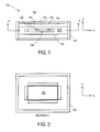
- FIGs. 1 and 2 respectively show side and top cross-section views of a storage device 100, with which an electrostatic drive according to the invention may be used.
- Storage device 100 includes a number of field emitters, such as 102 and 104, a storage medium 106 with a number of storage areas, such as 108, and a microactuator 110, which scans (moves) the storage medium 106 with respect to the field emitters or vice versa.
- Storage device 100 may be configured so that each storage area is responsible for storing one bit or many bits of information.
- the field emitters may be configured as point-emitters having very sharp points.
- each field emitter may have a radius of curvature of about one nanometer to hundreds of nanometers.
- a preselected potential difference is applied between a field emitter and its corresponding gate, such as between emitter 102 and circular gate 103 surrounding emitter 102. Due to the sharp point of the emitter, an electron beam current is extracted from the emitter and directed with a high degree of precision towards the storage area.
- electron optics may be desired to focus the electron beams.
- a voltage may also be applied to storage medium 106 to either accelerate or decelerate the field-emitted electrons or to aid in focusing the field-emitted electrons. Because the field emitters are used to access desired storage areas on the storage medium, the field emitters will also be referred to herein as access devices.
- Casing 120 typically is adapted to maintain storage medium 106 in partial vacuum, such as at least 10 -5 torr.
- partial vacuum such as at least 10 -5 torr.
- researchers have produced microfabricated field emitters in vacuum cavities using semiconductor processing techniques. See, for example, “Silicon Field Emission Transistors and Diodes,” by Jones, published in IEEE Transactions on Components, Hybrids and Manufacturing Technology, 15, page 1051, 1992.
- Each field emitter may correspond to one or more storage areas provided on storage medium 106. Where each field emitter is responsible for a number of storage areas, storage device 100 typically is adapted to scan or otherwise effect relative movement between casing 120 (and thus, the field emitters) and storage medium 106. For example, microactuator 110 typically is adapted to scan medium 106 to different location, so that each field emitter is positioned above different storage areas. With such a configuration, microactuator 110 can be used to scan an array (typically two-dimensional) of field emitters over the storage medium.
- casing 120 Because storage medium 106 moves relative to casing 120, it will at times be referred to as the "mover.” Correspondingly, casing 120 and various other components that are fixed relative to the casing (e.g., the field emitters) will be at times referred to as the "stator.”
- the field emitters typically are configured to read and/or write information on the storage areas via electron beams they produce.
- field emitters suitable for use with storage device 100 must produce electron beams narrow enough to achieve the desired bit density on storage medium 106. Further, the field emitters must provide electron beams of sufficient power density to perform the desired read/write operations.
- a variety of methods may be used to fabricate such field emitters. For example, one method is disclosed in "Physical Properties of Thin-Film Field Emission Cathodes With Molybdenum Cones," by Spindt et al, published in the Journal of Applied Physics, Vol. 47, No. 12, December 1976.
- the field emitters may be provided as a two-dimensional array (e.g., 100 by 100 emitters), with an emitter pitch of 50 micrometers in both the x-and the y-directions.
- Each emitter may access bits in tens of thousands to hundreds of millions of storage areas.
- the emitters may scan over (i.e., move relative to) a storage medium that has a two dimensional array of storage areas, where the periodicity between adjacent storage areas is anywhere from a fraction of a nanometer to 100 or more nanometers, and where the operational range of the microactuator is 50 micrometers in both the x and y-directions.
- the field emitters may be addressed simultaneously or in a multiplexed manner. Parallel addressing schemes may provide storage device 100 with significant performance enhancements in terms of access time and data rate.
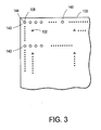
- Fig. 3 is a top view of an exemplary storage medium 106, depicting a two dimensional array of storage areas and a two dimensional array of field emitters. External circuitry (not shown) is used to address the storage areas. As indicated, it will often be desirable to segment the storage medium into rows, such as row 140, where each row contains a number of storage areas, such as storage area 108. Typically, each emitter is responsible for a number of rows, but is not responsible for the entire length of those rows. For example, as depicted, emitter 102 is responsible for the storage areas within rows 140 through 142, and within columns 144 through 146.
- Fig. 4 depicts an electrostatic drive 150 according to the present invention, including a number of mover electrodes 152 secured to mover 154 (e.g., storage medium 106), a number of stator electrodes 156 secured to stator 158 (e.g., casing 120), and a driver 160.
- mover electrodes 152 secured to mover 154
- stator electrodes 156 secured to stator 158
- driver 160 Typically, as indicated, both the mover electrodes and stator electrodes are disposed in a linear configuration which is parallel to the motion axis (e.g., the x-axis).
- Driver 160 causes voltages to arise at mover electrodes 152 and/or stator electrodes 156, which results in application of electrostatic forces between mover 154 and stator 158.
- the electrostatic forces cause the mover to move along the x-axis relative to the stator, as indicated. Varying the voltages applied to the electrodes produces changes in relative position of the mover and stator.
- the depicted arrangement is reproduced for that axis or direction.
- the depicted electrostatic drive system will include mover and stator electrodes along both the x- and y-axes.
- the scope of the invention includes systems capable of producing motion in multiple directions, including linear/axial motion and motion in curved directions or directions of other shapes.
- any desired number of electrodes may be used, in a variety of geometrical configurations.
- the mover and stator electrodes are normally arranged in a line parallel to the desired axis of motion. Also, it will usually be desirable to provide enough electrodes so that, over the entire desired range of motion, at least some of the mover and stator electrodes are close enough to generate enough electrostatic force to cause relative motion between the objects.
- mover electrodes 152 are provided at a uniform pitch, or spacing, along substantially the entire available length of the downward facing surface of mover 154.
- Voltage at each mover electrode 152 is indicated as being either 1 or 0, where 1 represents that the electrode is at a HI voltage level Ve, and where 0 represents that the electrode is at a LO voltage level, typically ground.
- voltages on the mover electrodes alternate between 1 and 0 for adjacent electrodes.
- a Ve of 40 volts has proven suitable, though other voltage levels may be used as appropriate to a particular implementation.
- the voltages at the mover electrodes do not change. Rather, as will be explained, the voltages on the stator electrodes are varied to produce the varying electrostatic forces used to move the mover relative to the stator.
- stator electrodes 156 are similarly arranged in linear fashion along a surface of stator 158 that faces mover 154. Like the mover electrodes, stator electrodes 156 typically are uniformly spaced from each other, that is, they have a uniform pitch. However, as will be seen, the stator electrode spacing may be different from the mover electrode spacing.
- phase transition from one phase to a sequentially adjacent phase causes mover 154 to move relative to stator 158 by a fixed step size.
- stator electrodes are both logically and physically grouped.
- the stator electrodes are physically grouped because each group includes seven stator electrodes that are physically adjacent one another on the stator. They are logically grouped because the group of seven is the smallest grouping of stator electrodes for which the electrical activity repeats identically over the entire length of the electrode surface. Each group receives the same set of signals from driver 160.
- stator electrodes For each grouping 163 of seven stator electrodes, there are six mover electrodes occupying the same length on the mover, as indicated. Thus, the pitch of the stator electrodes is 6/7 that of the mover electrodes. Other groupings and pitch ratios may be used. For example, the system may be configured so that the stator electrodes are organized into logical groupings of more or less than seven electrodes. The ratio of the pitch of the stator electrodes to the mover electrodes may be 1:1 or another value other than the 7:6 ratio of the depicted example.
- stator-mover pitch ratio be (n):(n-1), where n is the number of stator electrodes per logical/physical group.
- the mover step size per phase advancement is a function of the motor electrode geometry and the relative force constants of the motor spring and electrostatic drive. It will be appreciated that, for the above stator-mover pitch ratio of (n):(n-1), each transition to an adjacent phase results in a fixed step size equal to the pitch of the mover electrodes divided by the number of stator electrodes per logical/physical group. This assumes that the electrostatic force produced between the electrodes is much larger than the motor spring force.
- the step size will be 0.2 micrometers.
- changing the stator electrode voltages from phase 5 to either phase 4 or 6 will result in 0.2 micrometers of relative x-axis displacement between mover 154 and stator 158. Indeed, in this example, starting from any of the 14 different phases shown in table 162, incrementing or decrementing the phase by one will cause 0.2 micrometers of displacement.
- the step size produced by the above electrode geometry is adequate. In others, it is desirable to increase the resolution of the mover (e.g., by decreasing the step size).
- the data tracks on storage medium are 40 nanometers wide, or 1/5 of the 0.2 micrometer step size in the above example. To accurately access data tracks of this size, a much higher mover resolution than 0.2 micrometers is needed. Positioning at higher resolutions permits effective use of closed-loop servo control, reduces quantization errors, and permits operation of the storage device in track offset modes, as is often required for data recovery operations.
- the voltage on the second stator electrode (S1) can be proportionally increased from 0 to 1, while leaving all of the other stator electrodes at their phase 1 values, to achieve finer resolution position control.
- the proportional electrode switches with each phase advancement.
- S0 is proportionally controlled for phase 0, S1 for phase 1, S2 for phase 2, and so on.
- the proportional electrode is equal to (phase mod 7).
- Fig. 5 shows voltage waveforms for each of the seven stator electrodes in a particular stator electrode group. As the system cycles through each of the 14 different phases, each stator electrode is at the LO level (0) for six consecutive phases, transitions through one phase, and then is at the HI level (1) for six consecutive phases.
- the depicted waveforms show linear, ramped transitions between the LO and HI levels, indicating that the given stator electrode is proportionally controlled during the phase in which the ramped transition occurs.
- phase 9 the S2 electrode is proportionally controlled, and transitions from LO to HI.
- S2 is proportionally set to some scaled value between the LO and HI level in order to achieve the desired amount of displacement, while all of the other electrodes remain at the HI and LO levels specified by phase 9. Again, this may be thought of as a modification of phase 9.
- S2 is set at 0 (LO)
- phase 9 is unmodified from the voltage state shown in table 162 of Fig. 4.
- phase 9 is modified by increasing the voltage on S2, a proportional amount of displacement occurs, that is, proportional to the fixed step size that would occur by a simple transition from phase 9 to phase 10.
- the first is the phase. As discussed above, the phase determines which of the electrodes is to be proportionally controlled, and whether a HI or a LO level is to be applied to the remaining non-proportional electrodes.
- the second piece of information is the voltage that is to be applied to the proportional electrode in order to produce the desired mover displacement.
- exemplary control command 170 which includes an integer value 172 and a fractional value 174.
- Integer value 172 specifies the number of phase steps (the displacement resulting from a phase advancement) the mover is to move from some reference point. In the above example, each phase step provided 0.2 micrometers of displacement.
- the depicted integer value 172 is an 8-bit number, thus accommodating up to 256 phase steps. This would provide roughly a 50 micrometer operative range of relative displacement, assuming the 0.2 micrometer step size discussed above. This range has proved useful for the exemplary storage device discussed above.
- the bit-size of the integer value field can of course be modified to accommodate any desired number of phase steps.
- driver 160 typically cycles stator electrodes 156 through all of the intervening sequential phases.
- Fractional value 174 specifies the fractional value of a given phase step, and is used to scale the voltage which is applied to the proportionally controlled electrode. Another way of thinking about fractional value 174, is that it is a specification of how much a given phase is modified from the unmodified representation depicted in table 162. In depicted control command 170, a 12-bit fractional value is used, yielding an ultimate step size that is 4096 times smaller than the basic step size produced by a phase advancement. Accordingly, using the 0.2 micrometer phase step of the above examples, the 12-bit fractional value provides mover resolution to 0.05 nanometers (0.2 micrometers / 4096), or 1/20 of a nanometer.
- the proportion control system and control command described above provide a number of advantages.
- One such advantage is ease of operation.
- the described system acts as a digital to analog converter, which receives a digital input (e.g., control command 170) and produces an analog output (e.g., physical displacement of mover 154) in response.
- the amount of physical displacement is easily controlled, because it varies linearly with the value of the digital input.
- the control command allows the system programmer/designer to easily program motion control without knowledge of the underlying mechanical details of the movable system.
- the described proportional control scheme enhances movement resolution, without requiring additional electrodes or complex supporting electronics.
- Fig. 6 depicts various components of driver 160 that may be used to produce the desired voltages on stator electrodes 156.
- a half bridge 180 is provided for each of the stator electrodes. Each half bridge includes an input gate 182 coupled to a P-FET 184 and an N-FET 186, with accompanying connections to ground and Ve, and an output pin 188 for the stator electrode voltage.
- a regulating op-amp 190 is provided to achieve proportional control of one of the electrodes (e.g., the proportionally controlled electrode specified by the dashed diagonal lines in table 162).
- a voltage divider 192 (resistors 194 and 196) and a D-A converter 198 are coupled to the inputs of the op-amp.
- Electrode table 162 is the same table depicted in Fig. 4, and contains the voltage levels to be applied to the various stator electrodes.
- Driver 160 may further include a processor 202, memory 204, and other hardware and software components configured to perform the functions described herein.
- control command 170 is applied to driver 160 as an input.
- integer value 172 specifies a number of phase steps and the phase(s) in which the stator electrodes must be placed to achieve the commanded movement.
- the voltages to be applied to the non-proportional stator electrodes are known. Typically, these voltages are applied based on stored values, such as the values shown in table 162 (Fig. 4) for the various phases.
- the phase selection causes inputs to the non-proportional electrodes to be switched, such that the stored values are supplied as inputs to the half bridges which control the electrode outputs. Specifically, either a 1 or 0 is applied to input gate 182 of the half bridge for each of the non-proportional electrodes. Where a 1 is applied, P-FET 184 saturates, tying electrode output 188 to Ve. If a 0 is applied to the gate, N-FET 186 saturates, grounding the electrode output.
- the value of the phase also determines the switching of input signals to the proportional electrode. Specifically, the phase determines which of the half bridges will be selectively coupled with regulating op-amp 190, in order to produce an output between ground and Ve at the output of the half bridge. Based on the phase selection, input gate 182 of the selected half bridge is coupled with the output 208 of op-amp 190. Output 188 of the selected half bridge is coupled to the input side of op-amp 190 through resistor 196.
- the desired proportional voltage is produced at the output of the selected half bridge by supplying D-A converter 198 with input 210.
- Input 210 is set at either: (1) fv/4096, where fv is fractional value 174 (assuming fractional value 174 is a 12-bit number), or (2) 1-fv/4096. These two cases respectively reflect that displacement is sometimes incremented by increasing voltage on the proportional electrode (case 1), and at other times it is incremented by decreasing voltage on the proportional electrode (case 2).
- D-A converter 198 is provided with fv/4096 (case 1). Where the transitional slope is negative (when the Fig. 4 table entry for the electrode is a 1), D-A converter 198 is provided with 1-fv/4096 (case 2).
- the resulting analog output from D-A converter 198 is applied as an input to op-amp 190 via the positive terminal, along with the voltage-divided output from the selected half bridge, which is provided via the negative terminal.
- Application of these inputs eventually results in op-amp 190 reaching an equilibrium, at which point the desired proportion voltage is output from the selected half bridge and applied to the given stator electrode.
Landscapes
- Micromachines (AREA)
- Linear Motors (AREA)
Abstract
Description
Claims (10)
- An electrostatic drive 150, comprising:where transition from one voltage state to a sequentially adjacent voltage state produces a step size of relative movement between the mover 154 and stator 158,a mover 154 and a plurality of mover electrodes 152 operatively affixed thereto;a stator 158 and a plurality of stator electrodes operatively affixed thereto, the mover and stator being movable relative to one another via electrostatic force generated between the mover electrodes 152 and the stator electrodes 156; anda driver 160 configured to drive the stator electrodes 156 into any of a plurality of sequential voltage states, each voltage state being defined by a combination of LO and HI voltage levels existing at the stator electrodes,
where, for each of the voltage states, the driver 160 is further configured to selectively vary voltage applied at one of the stator electrodes to an amount between the LO and the HI voltage levels, in order to produce a proportionally smaller step size. - The electrostatic drive of claim 1, where the driver 160 is configured to produce relative movement between the mover 154 and stator 158 based on a digital control command 170, the driver 160 being further configured to produce relative movement between the mover 154 and stator 158 that varies linearly with the digital control 170 command.
- The electrostatic drive 150 of claim 2, where the digital control command 170 includes specification of one of the plurality of sequential voltage states.
- The electrostatic drive 150 of claim 2, where the digital control command 170 includes specification of one or more of the stator electrodes 156 that are to receive a varied voltage which is between the LO and the HI voltage levels.
- The electrostatic drive 150 of claim 4, where the digital control command 170 includes, for the one or more stator electrodes 156 that are to receive a varied voltage which is between the LO and the HI voltage levels, specification of the degree to which such varied voltage varies from either the HI voltage level or the LO voltage level.
- A electrostatic drive 150 as claimed in any preceding claim where the mover electrodes 152 are spaced uniformly from each other, and where the stator electrodes 156 are spaced uniformly from each other.
- The electrostatic drive 150 of claim 6, where the spacing between stator electrodes 156 is (N-1)/N times the spacing between the mover electrodes 152.
- The electrostatic drive 150 of claim 7, where N = 7.
- An electrostatic drive 150, comprising:where the driver 160 is configured so that varying the scalable level between the HI and LO levels proportionally adjusts the relative movement occurring between the objects 154, 158.a pair of objects 154, 158 configured to move relative to one another;a plurality of electrodes 156 operatively secured to one of the objects, the electrodes being configured so that application of voltages to the electrodes 156 creates electrostatic forces which effect relative movement of the objects 154, 158; anda driver 160 configured to selectively apply a voltage level to each of the electrodes 156, the voltage level being selected from the group consisting of a HI level, a LO level, and a scalable level from a range including levels between the HI and LO level, wherethe HI level or the LO level is applied to at least one of the electrodes 156; andthe scalable level is applied to at least one of the other electrodes 156,
- An electrostatically-driven computer storage device 100, comprising:where, for each of the voltage states, the driver 160 is further configured to selectively vary voltage applied at one of the access device electrodes 156 to an amount between the LO and the HI voltage levels, in order to produce a proportionally smaller step size and thereby increase resolution of the relative movement occurring between the storage medium 154 and access device 102, 158.a storage medium 154 and a plurality of storage medium electrodes 152 operatively affixed thereto;an access device 102, 158 movably coupled with the storage medium 154, the access 102, 158 device being configured to access storage locations 108 on the storage medium 154;a plurality of access device electrodes 156 that are fixed relative to the access device 102, 158, the storage medium 154 and access device 102, 158 being movable relative to one another via electrostatic force generated between the storage medium electrodes 152 and the access device electrodes 156; anda driver 160 configured to drive the access device electrodes 156 into any of a plurality of sequential voltage states, each voltage state being defined by a combination of LO and HI voltage levels existing at the access device electrodes 156, where transition from one voltage state to a sequentially adjacent voltage state produces a step size of relative movement between the storage medium and the access device,
Applications Claiming Priority (2)
| Application Number | Priority Date | Filing Date | Title |
|---|---|---|---|
| US43971 | 1979-05-30 | ||
| US10/043,971 US6747863B2 (en) | 2002-01-11 | 2002-01-11 | Electrostatic drive |
Publications (2)
| Publication Number | Publication Date |
|---|---|
| EP1330017A2 true EP1330017A2 (en) | 2003-07-23 |
| EP1330017A3 EP1330017A3 (en) | 2003-12-10 |
Family
ID=21929861
Family Applications (1)
| Application Number | Title | Priority Date | Filing Date |
|---|---|---|---|
| EP03250163A Withdrawn EP1330017A3 (en) | 2002-01-11 | 2003-01-10 | Electrostatic drive |
Country Status (7)
| Country | Link |
|---|---|
| US (1) | US6747863B2 (en) |
| EP (1) | EP1330017A3 (en) |
| JP (1) | JP2003260698A (en) |
| KR (1) | KR100927527B1 (en) |
| CN (1) | CN100380800C (en) |
| SG (1) | SG106111A1 (en) |
| TW (1) | TWI278175B (en) |
Cited By (1)
| Publication number | Priority date | Publication date | Assignee | Title |
|---|---|---|---|---|
| KR100927527B1 (en) * | 2002-01-11 | 2009-11-17 | 타이완 세미콘덕터 매뉴팩쳐링 컴퍼니 리미티드 | Blackout Drives and Blackout Drive Computer Storage Devices |
Families Citing this family (15)
| Publication number | Priority date | Publication date | Assignee | Title |
|---|---|---|---|---|
| US20070121477A1 (en) * | 2006-06-15 | 2007-05-31 | Nanochip, Inc. | Cantilever with control of vertical and lateral position of contact probe tip |
| US20070291623A1 (en) * | 2006-06-15 | 2007-12-20 | Nanochip, Inc. | Cantilever with control of vertical and lateral position of contact probe tip |
| US20070290282A1 (en) * | 2006-06-15 | 2007-12-20 | Nanochip, Inc. | Bonded chip assembly with a micro-mover for microelectromechanical systems |
| US7808061B2 (en) * | 2006-07-28 | 2010-10-05 | Hewlett-Packard Development Company, L.P. | Multi-die apparatus including moveable portions |
| US20080074984A1 (en) * | 2006-09-21 | 2008-03-27 | Nanochip, Inc. | Architecture for a Memory Device |
| US20080074792A1 (en) * | 2006-09-21 | 2008-03-27 | Nanochip, Inc. | Control scheme for a memory device |
| DE102008043836A1 (en) * | 2008-11-19 | 2010-05-20 | Robert Bosch Gmbh | Method of operating an electrostatic drive and electrostatic drives |
| US8368490B2 (en) * | 2008-12-18 | 2013-02-05 | Analog Devices, Inc. | Micro-electro-mechanical switch beam construction with minimized beam distortion and method for constructing |
| US8294539B2 (en) | 2008-12-18 | 2012-10-23 | Analog Devices, Inc. | Micro-electro-mechanical switch beam construction with minimized beam distortion and method for constructing |
| US8102637B2 (en) * | 2009-07-22 | 2012-01-24 | Analog Devices, Inc. | Control techniques for electrostatic microelectromechanical (MEM) structure |
| US8587328B2 (en) * | 2009-08-25 | 2013-11-19 | Analog Devices, Inc. | Automatic characterization of an actuator based on capacitance measurement |
| US10591318B2 (en) | 2017-08-31 | 2020-03-17 | Invensense, Inc. | Half-bridge circuit for a sensor |
| CN111508535B (en) | 2020-03-13 | 2021-08-13 | 华为技术有限公司 | A data writing and reading method, device and system |
| CN111313740B (en) * | 2020-04-03 | 2021-09-07 | 南京航空航天大学 | A three-phase linear electrostatic motor and control method |
| CN113541437A (en) * | 2021-06-01 | 2021-10-22 | 南方科技大学 | Electrostatic stepping motor |
Family Cites Families (17)
| Publication number | Priority date | Publication date | Assignee | Title |
|---|---|---|---|---|
| US3968416A (en) * | 1974-07-01 | 1976-07-06 | The Superior Electric Company | Motor control for a stepping motor |
| US4121145A (en) * | 1977-02-25 | 1978-10-17 | The Perkin-Elmer Corporation | High resolution stepping motor drive |
| JPS5869499A (en) * | 1981-10-20 | 1983-04-25 | Fuji Xerox Co Ltd | Exciting system for step motor |
| US5557596A (en) | 1995-03-20 | 1996-09-17 | Gibson; Gary | Ultra-high density storage device |
| US5986381A (en) * | 1997-03-14 | 1999-11-16 | Hewlett-Packard Company | Electrostatic actuator with spatially alternating voltage patterns |
| CA2349842C (en) | 1998-11-06 | 2005-09-06 | Honeywell Inc. | Driving method for electrostatic actuators |
| JP2000317898A (en) * | 1999-03-05 | 2000-11-21 | Ngk Insulators Ltd | Piezoelectric/electrostrictive device |
| US6215222B1 (en) * | 1999-03-30 | 2001-04-10 | Agilent Technologies, Inc. | Optical cross-connect switch using electrostatic surface actuators |
| US6373682B1 (en) * | 1999-12-15 | 2002-04-16 | Mcnc | Electrostatically controlled variable capacitor |
| US6496351B2 (en) * | 1999-12-15 | 2002-12-17 | Jds Uniphase Inc. | MEMS device members having portions that contact a substrate and associated methods of operating |
| KR100398856B1 (en) | 2000-03-30 | 2003-09-19 | 가부시끼가이샤 도시바 | Electrostatic actuator mechanism, driving method of the same, and camera module using the same |
| US6437965B1 (en) * | 2000-11-28 | 2002-08-20 | Harris Corporation | Electronic device including multiple capacitance value MEMS capacitor and associated methods |
| US6625004B1 (en) * | 2001-08-31 | 2003-09-23 | Superconductor Technologies, Inc. | Electrostatic actuators with intrinsic stress gradient |
| US6747863B2 (en) * | 2002-01-11 | 2004-06-08 | Hewlett-Packard Development Company, L.P. | Electrostatic drive |
| US6549394B1 (en) * | 2002-03-22 | 2003-04-15 | Agilent Technologies, Inc. | Micromachined parallel-plate variable capacitor with plate suspension |
| US6600644B1 (en) * | 2002-09-03 | 2003-07-29 | Industrial Technology Research Institute | Microelectronic tunable capacitor and method for fabrication |
| JP3822596B2 (en) * | 2003-12-08 | 2006-09-20 | 株式会社東芝 | Electrostatic actuator and driving method thereof |
-
2002
- 2002-01-11 US US10/043,971 patent/US6747863B2/en not_active Expired - Lifetime
- 2002-11-08 SG SG200206768A patent/SG106111A1/en unknown
- 2002-11-11 TW TW091133074A patent/TWI278175B/en not_active IP Right Cessation
-
2003
- 2003-01-06 JP JP2003000597A patent/JP2003260698A/en active Pending
- 2003-01-10 EP EP03250163A patent/EP1330017A3/en not_active Withdrawn
- 2003-01-10 KR KR1020030001599A patent/KR100927527B1/en not_active Expired - Lifetime
- 2003-01-13 CN CNB031016030A patent/CN100380800C/en not_active Expired - Lifetime
Cited By (1)
| Publication number | Priority date | Publication date | Assignee | Title |
|---|---|---|---|---|
| KR100927527B1 (en) * | 2002-01-11 | 2009-11-17 | 타이완 세미콘덕터 매뉴팩쳐링 컴퍼니 리미티드 | Blackout Drives and Blackout Drive Computer Storage Devices |
Also Published As
| Publication number | Publication date |
|---|---|
| CN100380800C (en) | 2008-04-09 |
| SG106111A1 (en) | 2004-09-30 |
| CN1433133A (en) | 2003-07-30 |
| JP2003260698A (en) | 2003-09-16 |
| KR20030061348A (en) | 2003-07-18 |
| TWI278175B (en) | 2007-04-01 |
| EP1330017A3 (en) | 2003-12-10 |
| TW200301991A (en) | 2003-07-16 |
| US6747863B2 (en) | 2004-06-08 |
| KR100927527B1 (en) | 2009-11-17 |
| US20030133252A1 (en) | 2003-07-17 |
Similar Documents
| Publication | Publication Date | Title |
|---|---|---|
| US6747863B2 (en) | Electrostatic drive | |
| US5563465A (en) | Actuator | |
| US6803699B2 (en) | Drive mechanism employing electromechanical transducer and drive method therefor | |
| JP4143420B2 (en) | Capacitance type position sensor | |
| US6700853B2 (en) | Data storage devices with wafer alignment compensation | |
| EP0381113B1 (en) | Tunnel current data storage apparatus having separate lever bodies | |
| Toshiyoshi et al. | Microelectromechanical digital-to-analog converters of displacement for step motion actuators | |
| JP2008175823A (en) | Drive stage, scanning probe microscope, information recording / reproducing device, processing device | |
| CN107786120B (en) | Piezoelectric rotary positioning platform with macro-micro hybrid motion characteristics and control method | |
| EP1350275B1 (en) | Double electromechanical element | |
| US6657444B2 (en) | Capacitance-based position sensor with integrating demodulator | |
| JPS60234477A (en) | Piezoelectric rotary device | |
| US20030117152A1 (en) | Digital control loop to solve instability of electrostatic drives beyond 1/3 gap limit | |
| JP2005312229A (en) | Drive apparatus and drive method | |
| US20090001846A1 (en) | Electrostatic Surface Drive With Multiple Operating Voltages | |
| US20030222661A1 (en) | Capacitance-based position sensor with integrating demodulator | |
| Sarajlic et al. | Design and modeling of compliant micromechanism for mechanical digital‐to‐analog conversion of displacement | |
| GB2387018A (en) | Actuation in a high density storage module | |
| Sarajlic et al. | 12-bit microelectromechanical digital-to-analog converter of displacement: Design, fabrication and characterization | |
| KR100660185B1 (en) | Micro driver and its driving method | |
| US6943980B2 (en) | Electrostatic track following using patterned media | |
| JP3229606B2 (en) | Micro-step actuator using ladder type suspension mechanism | |
| Hiroshi Toshiyoshi et al. | A digital-to-analog converter of displacement by an integrated micromechanism | |
| KR100263762B1 (en) | Electrostatic Micro Actuator with Shield | |
| KR100563665B1 (en) | Ultra-compact drive stage and its driving method |
Legal Events
| Date | Code | Title | Description |
|---|---|---|---|
| PUAI | Public reference made under article 153(3) epc to a published international application that has entered the european phase |
Free format text: ORIGINAL CODE: 0009012 |
|
| AK | Designated contracting states |
Designated state(s): AT BE CH CY DE DK ES FI FR GB GR IE IT LI LU MC NL PT SE TR |
|
| AX | Request for extension of the european patent |
Extension state: AL LT LV MK RO SI |
|
| PUAL | Search report despatched |
Free format text: ORIGINAL CODE: 0009013 |
|
| AK | Designated contracting states |
Kind code of ref document: A3 Designated state(s): AT BE CH CY DE DK ES FI FR GB GR IE IT LI LU MC NL PT SE TR |
|
| AX | Request for extension of the european patent |
Extension state: AL LT LV MK RO SI |
|
| 17P | Request for examination filed |
Effective date: 20040405 |
|
| 17Q | First examination report despatched |
Effective date: 20040630 |
|
| AKX | Designation fees paid |
Designated state(s): DE GB IT |
|
| STAA | Information on the status of an ep patent application or granted ep patent |
Free format text: STATUS: THE APPLICATION IS DEEMED TO BE WITHDRAWN |
|
| 18D | Application deemed to be withdrawn |
Effective date: 20060817 |