EP1329913A1 - Magnetic semiconductor material and method for preparation thereof - Google Patents
Magnetic semiconductor material and method for preparation thereof Download PDFInfo
- Publication number
- EP1329913A1 EP1329913A1 EP01961155A EP01961155A EP1329913A1 EP 1329913 A1 EP1329913 A1 EP 1329913A1 EP 01961155 A EP01961155 A EP 01961155A EP 01961155 A EP01961155 A EP 01961155A EP 1329913 A1 EP1329913 A1 EP 1329913A1
- Authority
- EP
- European Patent Office
- Prior art keywords
- semiconductor material
- magnetic semiconductor
- cdgep
- single crystal
- magnetic
- Prior art date
- Legal status (The legal status is an assumption and is not a legal conclusion. Google has not performed a legal analysis and makes no representation as to the accuracy of the status listed.)
- Withdrawn
Links
Images


Classifications
-
- H—ELECTRICITY
- H01—ELECTRIC ELEMENTS
- H01F—MAGNETS; INDUCTANCES; TRANSFORMERS; SELECTION OF MATERIALS FOR THEIR MAGNETIC PROPERTIES
- H01F41/00—Apparatus or processes specially adapted for manufacturing or assembling magnets, inductances or transformers; Apparatus or processes specially adapted for manufacturing materials characterised by their magnetic properties
- H01F41/14—Apparatus or processes specially adapted for manufacturing or assembling magnets, inductances or transformers; Apparatus or processes specially adapted for manufacturing materials characterised by their magnetic properties for applying magnetic films to substrates
- H01F41/20—Apparatus or processes specially adapted for manufacturing or assembling magnets, inductances or transformers; Apparatus or processes specially adapted for manufacturing materials characterised by their magnetic properties for applying magnetic films to substrates by evaporation
-
- C—CHEMISTRY; METALLURGY
- C30—CRYSTAL GROWTH
- C30B—SINGLE-CRYSTAL GROWTH; UNIDIRECTIONAL SOLIDIFICATION OF EUTECTIC MATERIAL OR UNIDIRECTIONAL DEMIXING OF EUTECTOID MATERIAL; REFINING BY ZONE-MELTING OF MATERIAL; PRODUCTION OF A HOMOGENEOUS POLYCRYSTALLINE MATERIAL WITH DEFINED STRUCTURE; SINGLE CRYSTALS OR HOMOGENEOUS POLYCRYSTALLINE MATERIAL WITH DEFINED STRUCTURE; AFTER-TREATMENT OF SINGLE CRYSTALS OR A HOMOGENEOUS POLYCRYSTALLINE MATERIAL WITH DEFINED STRUCTURE; APPARATUS THEREFOR
- C30B23/00—Single-crystal growth by condensing evaporated or sublimed materials
- C30B23/02—Epitaxial-layer growth
-
- C—CHEMISTRY; METALLURGY
- C30—CRYSTAL GROWTH
- C30B—SINGLE-CRYSTAL GROWTH; UNIDIRECTIONAL SOLIDIFICATION OF EUTECTIC MATERIAL OR UNIDIRECTIONAL DEMIXING OF EUTECTOID MATERIAL; REFINING BY ZONE-MELTING OF MATERIAL; PRODUCTION OF A HOMOGENEOUS POLYCRYSTALLINE MATERIAL WITH DEFINED STRUCTURE; SINGLE CRYSTALS OR HOMOGENEOUS POLYCRYSTALLINE MATERIAL WITH DEFINED STRUCTURE; AFTER-TREATMENT OF SINGLE CRYSTALS OR A HOMOGENEOUS POLYCRYSTALLINE MATERIAL WITH DEFINED STRUCTURE; APPARATUS THEREFOR
- C30B29/00—Single crystals or homogeneous polycrystalline material with defined structure characterised by the material or by their shape
- C30B29/10—Inorganic compounds or compositions
-
- H—ELECTRICITY
- H01—ELECTRIC ELEMENTS
- H01F—MAGNETS; INDUCTANCES; TRANSFORMERS; SELECTION OF MATERIALS FOR THEIR MAGNETIC PROPERTIES
- H01F1/00—Magnets or magnetic bodies characterised by the magnetic materials therefor; Selection of materials for their magnetic properties
- H01F1/01—Magnets or magnetic bodies characterised by the magnetic materials therefor; Selection of materials for their magnetic properties of inorganic materials
- H01F1/40—Magnets or magnetic bodies characterised by the magnetic materials therefor; Selection of materials for their magnetic properties of inorganic materials of magnetic semiconductor materials, e.g. CdCr2S4
- H01F1/401—Magnets or magnetic bodies characterised by the magnetic materials therefor; Selection of materials for their magnetic properties of inorganic materials of magnetic semiconductor materials, e.g. CdCr2S4 diluted
-
- H—ELECTRICITY
- H01—ELECTRIC ELEMENTS
- H01F—MAGNETS; INDUCTANCES; TRANSFORMERS; SELECTION OF MATERIALS FOR THEIR MAGNETIC PROPERTIES
- H01F10/00—Thin magnetic films, e.g. of one-domain structure
- H01F10/08—Thin magnetic films, e.g. of one-domain structure characterised by magnetic layers
- H01F10/10—Thin magnetic films, e.g. of one-domain structure characterised by magnetic layers characterised by the composition
- H01F10/18—Thin magnetic films, e.g. of one-domain structure characterised by magnetic layers characterised by the composition being compounds
- H01F10/193—Magnetic semiconductor compounds
Definitions
- the present invention relates to a magnetic semiconductor material and a method for preparing the same.
- an object of the present invention is to provide a magnetic semiconductor material having magnetization properties at room temperature and a method for preparing the magnetic semiconductor material.
- the present invention provides the following:
- a magnetic semiconductor material can be prepared which comprises a Group II-IV-V 2 compound semiconductor, used as a starting material, having a chalcopyrite structure and has ferromagnetism at room temperature.
- the elements of the Group II-IV-V 2 compound semiconductor are partially substituted by a transition element.
- Group II element in a Group II-VI compound semiconductor such as ZnS
- Group Ib and III elements When the Group II element in a Group II-VI compound semiconductor (such as ZnS) is regularly substituted by Group Ib and III elements, a Group I-III-VI 2 compound semiconductor containing three elements is obtained. Also, when the Group III element in a Group III-V compound semiconductor (such as GaAa) is regularly substituted by Group IIb and IV elements, a Group II-IV-V 2 compound semiconductor is obtained.
- the crystal structure of those semiconductors has tetragonal unit cells in which two unit cells having a sphalerite structure are laid one upon the other in the c axis direction.
- the tetragonal unit cells each contain 4 molecules (16 atoms) and the space group is expressed by D 2d 12 .
- This structure is the same as the structure of chalcopyrite CuFeS 2 and is, thus, referred to as chalcopyrite structure.
- Group II-IV-V 2 compound semiconductor crystal Eighteen types of Group II-IV-V 2 compound semiconductor crystal have been obtained in practice and they are ZnSiP 2 , ZnSiAs 2 , ZnSiSb 2 , ZnGeP 2 , ZnGeAs 2 , ZnGeSb 2 , ZnSnP 2 , ZnSnAs 2 , ZnSnSb 2 , CdSiP 2 , CdSiAs 2 , CdSiSb 2 , CdGeP 2 , CdGeAs 2 , CdGeSb 2 , CdSnP 2 , CdSnAs 2 , and CdSnSb 2 .
- the characteristics of the Group II-IV-V 2 semiconductors are similar to those of Group III-V semiconductors.
- the mobility is large and, for example, CdGeAs 2 has an electron mobility of 4000 cm 2 /Vs, which is as large as that of GaAs.
- the band gaps cover a wide range.
- ZnSiP has the largest band gap of 2.96 eV, and is therefore substantially transparent and colorless.
- CdGeP 2 has a band gap of 1.72 eV (at room temperature) and its thin crystal is light red. The melting points are very low. Since, for example, CdGeP 2 and CdGeAs 2 have melting points of 790°C and 670°C, respectively, their crystal growth seems to be easy. However, it is difficult to control the vapor pressures of P and As in practice.
- a II-IV-V 2 material whose absorption edge is in the visible region may provide a device capable of changing colors by applying a magnetic field.
- the II-IV-V 2 compound semiconductors advantageously exhibit a large magnetooptic effect in their absorption edges.
- An optical isolator for visible light can be manufactured making use of this characteristic feature, and holds a greater promise than known CdMnTe optical isolators.
- a spin transistor in which the degree of freedom of spin is increased to a semiconductor device can be provided in the future.
- a magnetic semiconductor material comprising CdMnGeP 2 and having magnetization properties at room temperature is prepared from, for example, a starting materials CdGeP 2 .
- the following describes a method for preparing a magnetic semiconductor material comprising CdMnGeP 2 of the present invention.
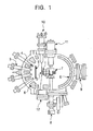
- Fig. 1 is a schematic illustration of a molecular beam epitaxy apparatus for a magnetic semiconductor material comprising CdMnGeP 2 according to an example of the present invention.
- reference numeral 1 designates a substrate holder and a substrate heater.
- Reference numeral 2 designates a CdGeP 2 single crystal set on the substrate holder 1.
- the apparatus also includes a molecular beam source 3, a shutter 4, a main shutter 5, a liquid nitrogen shroud 6, an ion gage 7, a substrate heater manipulator 8, a gate valve 9, a reflection high-energy electron diffraction apparatus (RHEED) 10, a mass spectroscope 11, and RHEED fluorescent screen 12.
- RHEED reflection high-energy electron diffraction apparatus
- Mn (not shown in the drawing) was vapor-deposited onto the CdGeP 2 single crystal 2 at a thickness of 200 or 300 ⁇ while the CdGeP 2 single crystal 2 was maintained at a temperature of 390°C in the molecular beam epitaxy apparatus 1. Then, the sample was heated at 510°C for 1 hour. The degree of vacuum during vapor-deposition and heating was on the order of 10 -8 Torr or less. The Mn deposition rate was set at 8 ⁇ /min.
- Fig. 2 is a representation of an high-energy electron diffraction (RHEED) pattern of a (112) plane of CdGeP 2 in the preparation process according to the example of the present invention.
- the incidence direction of the electron beam is [111]CdGeP 2 .
- Fig. 2 (a) shows a surface (390°C) of the CdGeP 2 before Mn vapor deposition and indicates that a clean plane of the CdGeP 2 appears on the surface.
- Fig. 2 (b) shows the surface (390°C) after Mn vapor deposition and indicates that the pattern is changed to a halo pattern showing an amorphous state. It is shown that the vapor-deposited Mn is accumulated on the surface.
- Fig. 2 (c) shows a pattern (C[111], 30 sec, 15 min) after heat treatment and suggests that spots appear again in the same position. It is shown that a CdGeP 2 crystal structure is maintained even after the deposited Mn is diffused into the CdGeP 2 .
- Fig. 3 is a graph showing a M-H loop of the CdMnGeP 2 at room temperature according to the example of the present invention.
- the horizontal axis represents the magnetic field H ( ⁇ 5 kOe) and the vertical axis represents the magnetization ( ⁇ 10 -3 e.m.u.).
- Fig. 3 (a) shows an M-H loop when a magnetic field is applied perpendicular to the surface
- Fig. 3 (b) shows an M-H loop when a magnetic field is applied parallel to the surface.
- Fig. 4 is a graph showing photoluminescence spectrums of GdMnGeP 2 (initially CdGeP 2 ) of the example of the present invention.
- the horizontal axis represents the photon energy (eV), and the vertical axis represents the photoluminescence (l/l max ).
- the CdMnGeP 2 is prepared by depositing CdGeP 2 and Mn at a thickness of 200 to 300 ⁇ .
- the band gap is about 1.6 eV before adding Mn (spectrum a), and that the peaks of the spectrums after depositing Mn at 200 to 300 ⁇ are shifted to the high energy side and the band gaps become larger (spectrums b and c).
- the sample in which Mn is deposited at 300 ⁇ is more greatly shifted (spectrum c).
- Fig. 5 is a graph showing an X-ray diffraction pattern of CdMnGeP 2 of the example of the present invention.
- the horizontal axis represents 2 ⁇ (degree) and the vertical axis represents the X-ray intensity (cps).
- the following describes a method for preparing a magnetic semiconductor material comprising ZnGeP 2 , according to the present invention.
- Mn is vapor-deposited and diffused at a thickness of 300 ⁇ onto a ZnGeP 2 single crystal while the ZnGeP 2 single crystal is maintained at a temperature of about 400°C in a molecular beam epitaxy apparatus. In this instance, heat treatment is not performed.
- a magnetic semiconductor material comprising ZnGeP 2 , having magnetization properties at room temperature is prepared using a ZnGeP 2 single crystal as a starting material.
- Fig. 6 is representations of high-energy electron diffraction (RHEED) patterns of ZnGeP 2 according to the example of the present invention.
- Fig. 6 (a) shows the surface of a ZnGeP 2 single crystal before Mn is vapor-deposited
- Fig. 6 (b) shows the surface after Mn has been deposited.
- the sample temperature is 400°C at this point. It is shown that the surface is flat and has good crystallinity before vapor deposition. Once Mn vapor deposition is started, the surface is gradually changed to a streak pattern. This indicates that the crystal structure is maintained during vapor deposition. It is considered from these results that Mn atoms are diffused into the ZnGeP 2 crystal as soon as they are deposited.
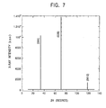
- Fig. 7 is a graph showing an X-ray diffraction pattern of ZdGeP 2 : Mn in which Mn is diffused.
- the horizontal axis represents 2 ⁇ (degree) and the vertical axis represents the X-ray intensity (cps).
- This X-ray diffraction pattern also shows only diffraction peaks from ZnGeP 2 having good crystallinity, and indicates that the crystal structure and lattice constant of the ZnMnGeP 2 is substantially the same as those of ZnGeP 2 .
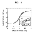
- Fig. 8 is a graph showing a magnetization curve (M-H loop) at 350 K of the ZnGeP 2 : Mn in which Mn is diffused.
- the horizontal axis represents the magnetic field H (kOe) and the vertical axis represents the magnetization (x 10 -5 e.m.u.).
- the present invention offers the following advantages:
- a magnetic semiconductor material having ferromagnetization properties at room temperature can be obtained.
- the magnetic semiconductor material has magnetization properties at room temperature.
- the magnetic semiconductor material has a band gap larger than that of CdMnTe, and it is, consequently, expected to be used for a magneto-optical element.
- an approximate Faraday rotation angle of -5.7 ⁇ 10 4 deg/cm was estimated at a wavelength of 709 nm.
- the Faraday rotation angle of paramagnetic CdMnTe generally used for optical isolators is proportional to the magnetic field and is 4 ⁇ 10 3 deg/cm at a magnetic field of 5 kOe.
- the ferromagnetic CdMnGeP 2 of the present invention has a Faraday rotation angle of 10 times or more that of CdMnTe at a magnetic field as small as 1.5 kOe which is needed to saturate the magnetization.
- the ZnMnGeP 2 of the present invention can also offer the same advantages as above.
- the magnetic semiconductor material of the present invention has magnetization properties at room temperature and a large band gap, and is thus suitably used for magneto-optical elements.
Landscapes
- Engineering & Computer Science (AREA)
- Chemical & Material Sciences (AREA)
- Power Engineering (AREA)
- Materials Engineering (AREA)
- Organic Chemistry (AREA)
- Metallurgy (AREA)
- Crystallography & Structural Chemistry (AREA)
- Manufacturing & Machinery (AREA)
- Inorganic Chemistry (AREA)
- Thin Magnetic Films (AREA)
- Hard Magnetic Materials (AREA)
- Hall/Mr Elements (AREA)
- Physical Deposition Of Substances That Are Components Of Semiconductor Devices (AREA)
Abstract
Description
Claims (6)
- A magnetic semiconductor material comprising a Group II-IV-V2 compound semiconductor, used as a starting material, having a chalcopyrite structure whose constituent elements are partially substituted by a transition element, the magnetic semiconductor material thereby having magnetization properties at room temperature.
- A magnetic semiconductor material according to Claim 1, wherein the Group II-IV-V2 compound semiconductor having the chalcopyrite structure is CdGeP2, and the transition element is Mn.
- A magnetic semiconductor material according to Claim 1, wherein the Group II-IV-V2 compound semiconductor having the chalcopyrite structure is ZnGeP2, and the transition element is Mn.
- A method for preparing a magnetic semiconductor material, comprising:(a) a vapor-deposition step of vapor-depositing Mn at a thickness of 200 to 300 Å onto a CdGeP2 single crystal while the CdGeP2 single crystal is maintained at a temperature of about 390°C in a molecular beam epitaxy apparatus; and(b) a heating step of heating the Mn-deposited CdGeP2 single crystal at a temperature of about 510°C for 1 hour to obtain a magnetic semiconductor comprising CdMnGeP2 and having magnetization properties at room temperature.
- A method for preparing a magnetic semiconductor material according to Claim 4, wherein the degree of vacuum in the vapor-deposition step and the heating step is on the order of 10-8 Torr or less.
- A method for preparing a magnetic semiconductor material, comprising:(a) a vapor deposition step of vapor-depositing and diffusing Mn at a thickness of about 300 Å onto a ZnGeP2 single crystal while the ZnGeP2 single crystal is maintained at a temperature of about 400°C in a molecular beam epitaxy apparatus,(b) whereby a magnetic semiconductor comprising ZnGeP2 and having magnetization properties at room temperature or more is obtained without heating after the vapor deposition step.
Applications Claiming Priority (3)
| Application Number | Priority Date | Filing Date | Title |
|---|---|---|---|
| JP2000261367 | 2000-08-30 | ||
| JP2000261367 | 2000-08-30 | ||
| PCT/JP2001/007408 WO2002019352A1 (en) | 2000-08-30 | 2001-08-29 | Magnetic semiconductor material and method for preparation thereof |
Publications (2)
| Publication Number | Publication Date |
|---|---|
| EP1329913A1 true EP1329913A1 (en) | 2003-07-23 |
| EP1329913A4 EP1329913A4 (en) | 2006-08-23 |
Family
ID=18749218
Family Applications (1)
| Application Number | Title | Priority Date | Filing Date |
|---|---|---|---|
| EP01961155A Withdrawn EP1329913A4 (en) | 2000-08-30 | 2001-08-29 | SEMICONDUCTOR MAGNETIC MATERIAL AND METHOD FOR PREPARING THE SAME |
Country Status (4)
| Country | Link |
|---|---|
| US (1) | US7102171B2 (en) |
| EP (1) | EP1329913A4 (en) |
| JP (1) | JP3773899B2 (en) |
| WO (1) | WO2002019352A1 (en) |
Cited By (2)
| Publication number | Priority date | Publication date | Assignee | Title |
|---|---|---|---|---|
| CN106637416A (en) * | 2016-12-28 | 2017-05-10 | 厦门大学 | Molecular beam epitaxy and in-situ characterization device under vector strong magnetic field |
| CN109841369A (en) * | 2017-11-24 | 2019-06-04 | 中国科学院物理研究所 | Dilute magnetic semiconductor material and preparation method thereof with giant magnetoresistance effect |
Families Citing this family (3)
| Publication number | Priority date | Publication date | Assignee | Title |
|---|---|---|---|---|
| US20060181197A1 (en) * | 2004-07-01 | 2006-08-17 | Kumio Nago | Electroluminescent device and display |
| JP5212684B2 (en) * | 2007-04-10 | 2013-06-19 | 株式会社Ihi | Magnetic semiconductor manufacturing method and manufacturing apparatus |
| US8084374B2 (en) * | 2009-11-19 | 2011-12-27 | Washington University In St. Louis | Tuning of photo-absorption materials through use of magnetic fields |
Family Cites Families (7)
| Publication number | Priority date | Publication date | Assignee | Title |
|---|---|---|---|---|
| US3719481A (en) * | 1970-03-07 | 1973-03-06 | Xerox Corp | Electrostatographic imaging process |
| JPS5474673A (en) * | 1977-11-28 | 1979-06-14 | Nippon Telegr & Teleph Corp <Ntt> | Semiconductor device |
| JP3337494B2 (en) * | 1992-07-24 | 2002-10-21 | 松下電器産業株式会社 | Method of manufacturing solar cell and thin-film solar cell |
| JP3068416B2 (en) * | 1994-08-26 | 2000-07-24 | 日本電気株式会社 | Information recording medium |
| JP2990036B2 (en) * | 1995-02-13 | 1999-12-13 | ティーディーケイ株式会社 | Optical recording medium and manufacturing method thereof |
| US5736657A (en) * | 1995-03-31 | 1998-04-07 | Ricoh Company, Ltd. | Sputtering target |
| KR100984585B1 (en) * | 2000-08-22 | 2010-09-30 | 프레지던트 앤드 펠로우즈 오브 하버드 칼리지 | Nanosensors |
-
2001
- 2001-08-29 JP JP2002524161A patent/JP3773899B2/en not_active Expired - Fee Related
- 2001-08-29 US US10/344,895 patent/US7102171B2/en not_active Expired - Fee Related
- 2001-08-29 EP EP01961155A patent/EP1329913A4/en not_active Withdrawn
- 2001-08-29 WO PCT/JP2001/007408 patent/WO2002019352A1/en not_active Ceased
Cited By (4)
| Publication number | Priority date | Publication date | Assignee | Title |
|---|---|---|---|---|
| CN106637416A (en) * | 2016-12-28 | 2017-05-10 | 厦门大学 | Molecular beam epitaxy and in-situ characterization device under vector strong magnetic field |
| CN106637416B (en) * | 2016-12-28 | 2018-11-20 | 厦门大学 | Molecular beam epitaxy and its in-situ characterization device under vector high-intensity magnetic field |
| CN109841369A (en) * | 2017-11-24 | 2019-06-04 | 中国科学院物理研究所 | Dilute magnetic semiconductor material and preparation method thereof with giant magnetoresistance effect |
| CN109841369B (en) * | 2017-11-24 | 2020-06-02 | 中国科学院物理研究所 | Diluted magnetic semiconductor material with giant magnetoresistance effect and preparation method thereof |
Also Published As
| Publication number | Publication date |
|---|---|
| WO2002019352A1 (en) | 2002-03-07 |
| US20040014244A1 (en) | 2004-01-22 |
| US7102171B2 (en) | 2006-09-05 |
| JP3773899B2 (en) | 2006-05-10 |
| EP1329913A4 (en) | 2006-08-23 |
Similar Documents
| Publication | Publication Date | Title |
|---|---|---|
| Tanaka et al. | Molecular beam epitaxy of MnAs thin films on GaAs | |
| Lu et al. | Reconstruction Control of Magnetic Properties during Epitaxial Growth<? format?> of Ferromagnetic Mn 3-δ Ga on Wurtzite GaN (0001) | |
| EP0400263B1 (en) | New class of magnetic materials for solid state devices | |
| EP1536432A1 (en) | Ferromagnetic iv group based semiconductor, ferromagnetic iii-v group based compound semiconductor, or ferromagnetic ii-iv group based compound semiconductor, and method for adjusting their ferromagnetic characteristics | |
| Koyanagi et al. | Epitaxial growth of Cd1− x Mn x Te films by ionized‐cluster beams and their magneto‐optical properties | |
| US4728178A (en) | Faceted magneto-optical garnet layer and light modulator using the same | |
| Higuchi et al. | Fabrications of cerium-substituted YIG thin films for magnetic field sensor by pulsed-laser deposition | |
| Keavney et al. | High-coercivity, c-axis oriented Nd 2 Fe 14 B films grown by molecular beam epitaxy | |
| Stadler et al. | Magneto-optical garnet films made by reactive sputtering | |
| US7102171B2 (en) | Magnetic semiconductor material and method for preparation thereof | |
| US6733587B2 (en) | Process for fabricating an article comprising a magneto-optic garnet material | |
| JPWO2002019352A1 (en) | Magnetic semiconductor material and its manufacturing method | |
| Hegde et al. | Sputter synthesis of TbCu7 type Sm (CoFeCuZr) films with controlled easy axis orientation | |
| US6351331B1 (en) | Faraday rotator and magneto-optical element using the same | |
| US5965287A (en) | Magneto-optical element material and Faraday element using the same | |
| Takeno et al. | Structure and Magnetic Properties of MnBi Thin Films | |
| Okamura et al. | Sputter epitaxy of cerium yttrium iron garnet films on neodymium gallium garnet substrates | |
| Park et al. | Selective-area micropatterning of liquid-phase epitaxy-grown iron garnet films | |
| US4876144A (en) | Single crystal thin film | |
| van Dover et al. | Magnetic properties of gd-substituted yttrium nitride | |
| Lee et al. | Controlled growth of ZnSeTe superlattices with sinusoidal compositional modulation | |
| JP2721869B2 (en) | Method for manufacturing diluted magnetic semiconductor thin film | |
| Friemel et al. | Coaligning arrays of air-sensitive single crystals for inelastic neutron scattering experiments | |
| US20040104415A1 (en) | Semiconductor array | |
| EP0166924A2 (en) | Faceted magneto-optical garnet layer |
Legal Events
| Date | Code | Title | Description |
|---|---|---|---|
| PUAI | Public reference made under article 153(3) epc to a published international application that has entered the european phase |
Free format text: ORIGINAL CODE: 0009012 |
|
| 17P | Request for examination filed |
Effective date: 20030320 |
|
| AK | Designated contracting states |
Designated state(s): AT BE CH CY DE DK ES FI FR GB GR IE IT LI LU MC NL PT SE TR |
|
| RIN1 | Information on inventor provided before grant (corrected) |
Inventor name: SATO, KATSUAKI Inventor name: ISHIBASHI, TAKAYUKI Inventor name: MEDVEDKIN, GENNADIY |
|
| RAP1 | Party data changed (applicant data changed or rights of an application transferred) |
Owner name: JAPAN SCIENCE AND TECHNOLOGY AGENCY |
|
| RBV | Designated contracting states (corrected) |
Designated state(s): DE FR GB NL |
|
| RAP1 | Party data changed (applicant data changed or rights of an application transferred) |
Owner name: JAPAN SCIENCE AND TECHNOLOGY AGENCY |
|
| A4 | Supplementary search report drawn up and despatched |
Effective date: 20060720 |
|
| 17Q | First examination report despatched |
Effective date: 20061019 |
|
| STAA | Information on the status of an ep patent application or granted ep patent |
Free format text: STATUS: THE APPLICATION IS DEEMED TO BE WITHDRAWN |
|
| 18D | Application deemed to be withdrawn |
Effective date: 20080901 |