EP1329903A1 - Halbleiter-Speichereinrichtung mit zum Schreibzugriff zugehöriger Kommandosequenz für die Umschaltung in eine Test-Betriebsart - Google Patents
Halbleiter-Speichereinrichtung mit zum Schreibzugriff zugehöriger Kommandosequenz für die Umschaltung in eine Test-Betriebsart Download PDFInfo
- Publication number
- EP1329903A1 EP1329903A1 EP02000941A EP02000941A EP1329903A1 EP 1329903 A1 EP1329903 A1 EP 1329903A1 EP 02000941 A EP02000941 A EP 02000941A EP 02000941 A EP02000941 A EP 02000941A EP 1329903 A1 EP1329903 A1 EP 1329903A1
- Authority
- EP
- European Patent Office
- Prior art keywords
- storage device
- memory device
- test mode
- flash memory
- command sequence
- Prior art date
- Legal status (The legal status is an assumption and is not a legal conclusion. Google has not performed a legal analysis and makes no representation as to the accuracy of the status listed.)
- Granted
Links
- 239000004065 semiconductor Substances 0.000 title 1
- 230000015654 memory Effects 0.000 claims description 96
- 208000033748 Device issues Diseases 0.000 claims 1
- 230000008901 benefit Effects 0.000 description 5
- 230000006870 function Effects 0.000 description 3
- 230000007257 malfunction Effects 0.000 description 3
- 230000002093 peripheral effect Effects 0.000 description 3
- 101100243442 Arabidopsis thaliana PER4 gene Proteins 0.000 description 2
- 241000146356 Komma Species 0.000 description 2
- 108010076504 Protein Sorting Signals Proteins 0.000 description 2
- 230000010354 integration Effects 0.000 description 2
- 230000007246 mechanism Effects 0.000 description 2
- 230000008878 coupling Effects 0.000 description 1
- 238000010168 coupling process Methods 0.000 description 1
- 238000005859 coupling reaction Methods 0.000 description 1
- 238000012217 deletion Methods 0.000 description 1
- 230000037430 deletion Effects 0.000 description 1
- 238000001514 detection method Methods 0.000 description 1
- 238000011161 development Methods 0.000 description 1
- 230000018109 developmental process Effects 0.000 description 1
- 230000004044 response Effects 0.000 description 1
Images
Classifications
-
- G—PHYSICS
- G11—INFORMATION STORAGE
- G11C—STATIC STORES
- G11C29/00—Checking stores for correct operation ; Subsequent repair; Testing stores during standby or offline operation
- G11C29/04—Detection or location of defective memory elements, e.g. cell constructio details, timing of test signals
- G11C29/08—Functional testing, e.g. testing during refresh, power-on self testing [POST] or distributed testing
- G11C29/12—Built-in arrangements for testing, e.g. built-in self testing [BIST] or interconnection details
- G11C29/46—Test trigger logic
Definitions
- the present invention relates to a device according to the Preamble of claim 1, i.e. a storage device for storing data, the storage device to test them in a particular test of the memory device enabling test mode is shiftable.
- Such a memory device is, for example, a flash memory.
- Flash memories have been in countless numbers for many years Embodiments are known and do not require any further explanation.
- Flash memory can either be implemented as separate components be, or in other building blocks such as be included in a microcontroller.
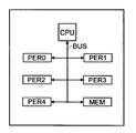
- a microcontroller with an internal flash memory is in shown in the figure.
- the microcontroller shown contains a CPU CPU, peripheral units PER0 to PER4, a flash memory MEM, and a bus connecting the components mentioned together BUS; the peripheral units PER0 to PER4 can for example a DMA controller, a timer, a serial interface, a parallel interface, an A / D converter, a D / A converter, or other components.
- each microcontroller component which can become bus master on the bus erase, write to and read out the flash memory MEM. How this happens in detail is known and does not require any detailed explanation.
- the flash memory MEM is also in a test mode relocatable, in which certain, in the normal Operation of the flash memory not or only with great effort feasible tests of the flash memory are feasible.
- Putting the flash memory MEM into the test mode takes place in the known building blocks that have a flash memory included, in that one or more pins of the the relevant block certain signals or signal sequences be created.
- RAMs random access memory
- ROMs read-only memory
- EPROMs erasable read-only memory
- EEPROMs electrically erasable read-only memory
- the present invention is therefore based on the object to find a way by which the probability that a storage device inadvertently into the Test mode is shifted to a minimum is.
- the storage device according to the invention is characterized by this from that the storage device by a certain Write access or a specific sequence of Comprehensive write access to the storage device Command sequence can be put into the test mode.
- the figure shows the structure of a storage device containing microcontroller.
- the storage device described below is a Flash memory. However, it is already at this point pointed out that in principle it is also any other memory, such as RAM, a ROM, an EPROM, an EEPROM, etc.
- the flash memory described is in the example considered Part of a microcontroller or other program-controlled Unit like a microprocessor or one Signal processor. However, it could also be part of any other building block, this building block also a (memory) block containing only the flash memory can be.
- microcontroller containing the flash memory can, for example that shown in the figure and already at the beginning microcontrollers described with reference thereto; in the considered example it is assumed that the in the Figure shown microcontroller of the one considered here Microcontroller containing flash memory.
- the bus master read the flash memory on the bus and delete.
- the CPU CPU is the microcontroller component that reads, describes, or flash memory extinguished.
- the explanations given here apply to the Case that another microcontroller component uses the flash memory reads, describes, or deletes accordingly.
- a command sequence consists of a sequence of write access to the flash memory, whereby the here addresses and data to be used by the respective Syntax of the operation to be initiated by the command sequence are specified.
- the command sequences are contained in the flash memory Command interpreter fed, and this decides based on the data received and / or the address used (or a certain part of it) what operation is to be carried out.
- the flash memory considered here can be replaced by a such a command sequence is also set to the test mode become.
- the command sequence through which the flash memory is put into the test mode is hereinafter referred to as Test mode entry command sequence called.
- Certain operations can be performed in the test mode be in the normal operation of the flash memory cannot be carried out. These operations include for example writing and / or reading out internal registers of flash memory, or creating certain Conditions for certain operations (also for im normal operation of the flash memory or in other operating modes executable operations). For example, but far from exclusively the proper one Function of an error detection unit and / or an error correction unit of the flash memory tested through which in the read out of the flash memory Data existing errors are recognized and / or corrected.
- test mode entry command sequence is executed as one "normal" command sequence. That is, it consists of a sequence several consecutive write accesses to the Flash memory, whereby these write accesses also from the previously mentioned command interpreter.
- the test mode entry command sequence can, for example, be the Write access sequence (hAA, h11) (hBB, h12) (hCC, h13) (hDD, h14).
- the feed has the test mode entry command sequence to the flash memory Consequence that the flash memory is put into a state in which through subsequent write accesses Flash memory operations can be initiated in normal operation of the flash memory, i.e. except for Test mode of the same can not be executed. It however, it should be noted at this point that additionally or alternatively, the Execution of these operations already through the test mode entry command sequence to cause.
- the test mode entry command sequence and preferably also the other commands or command sequences by which the Flash memory can be caused to perform operations is not executed outside of its test mode are preferably secret, i.e. the Flash memory users unknown.
- the flash memory the test mode entry command sequence and / or the other secret commands or command sequences treated externally as inadmissible, for example with the output of an error signal acknowledged. Even each one is preferred Write access to secret commands or command sequences treated like this. This means that after each write access to the Flash memory that is not one in the normal mode of the flash memory permissible write access sequence belong an error signal is output.
- the Test mode entry command sequence or in the test mode write access to the flash memory which occurs to a command or a command sequence heard or can belong to that in normal operation of the flash memory is executable, this write access automatic reset that is not visible from the outside the flash memory in the normal operating mode, and both externally and internally as permissible write access is treated and the assigned operations in Flash memory triggers. That is not it, or at least it is not easily possible, the test mode entry command sequence and the accesses permitted in the test mode trying to figure out the flash memory.
- the flash memory can preferably be opened when it is is in a so-called protected mode, not in the Move test mode.
- Write access is in protected mode and / or read accesses, or at least certain ones Microcontroller components write access and / or read access to the flash memory or certain Parts of it locked.
- the flash memory for example put in protected mode if prevented is that the memory content of the flash memory through this unauthorized persons are changed or read out can.
- the fact that the flash memory when it is in the Protected mode is not in the test mode the Protected Bypassed protection of flash memory or fashion can be canceled. In the example considered, that the protected mode by supplying a password sequence can be temporarily canceled, and that the flash memory when this has happened, as described in the test mode can be brought.
- the supply of the test mode entry command sequence to the flash memory has in the example considered that within of the flash memory comprising one or more bits Identifier is set. In the example considered there is this identifier from a particular bit of a particular Flash memory register. This bit is the following referred to as the test enable bit or TE bit.
- the set TE bit is the prerequisite for that in normal operation inaccessible registers or other memory of the flash memory can be read and / or written, and / or that test functions implemented in the flash memory can be activated. As long as the TE bit is set, the operations mentioned are carried out; if and so this is not possible as long as the TE bit is reset.
- the TE bit is preferably after the reset of the flash memory containing the block automatically reset, and the TE bit can only be set, by adding the test mode entry command sequence to the flash memory is fed.
- Resetting the TE bit is equivalent to exiting the test mode.
- the TE bit can be reset at the instigation of the user and / or automatically.
- Resetting the TE bit at the user's request can be done by appropriate write access to the flash memory by which the TE bit is reset becomes.
- the first way is that the TE bit is automatic is reset when a normal, i.e. an outside the test mode feasible access to the Flash memory is done.
- the second way is that the TE bit is automatic is reset if an invalid one is set when the TE bit is set
- the flash memory is accessed.
- the third way is that the TE bit is automatic is reset if after setting the TE bit a predetermined time has passed.
- the TE bit follows a reset of the same only after a reset of the Flash memory or the block containing it again can be set.
- the flash memory through various test mode entry command sequences is put into the test mode, it depends on the depends on the test mode entry command sequence used, which operations are performed in the test mode allowed to. This makes it possible for selected or all users to allow the flash memory to be limited Relocate test mode offering test options.
- test-mode entry command sequence could also be provided in the test-mode entry command sequence to integrate a password (similar to the above already user commands through which the temporary Protection mode is canceled). This would be under others, for example, open up the possibility of entering the test mode to arrive without first using the commands mentioned to leave protection mode.
- test mode entry password only knowledge of part of the test mode entry password or a derived quantity like for example, a signature derived from it is required. This would make it possible for a customer to buy one Flash memory with Read and / or Write Protection installed sends back to the manufacturer for analysis, the manufacturer would not have to reveal his full password.
- One of the advantages is that the test of the flash memory completely handled within the flash memory can be. There are no additional external ones Resources necessary. This will reduce the effort for System integration is reduced and especially integration facilitated in different system environments.
- test mode entry command sequence seamlessly in the case of flash memories inserts the existing structure of the command sequences, and also the read / write accesses carried out in the test mode to the flash memory over the existing ones Resources.
- test mode entry command sequence due to the error signals that the flash memory after every write access to it that does not to one of those permitted in normal operation of the flash memory Write access sequences can include, not even partially (by successive partial discovery) can.
Landscapes
- Storage Device Security (AREA)
- Techniques For Improving Reliability Of Storages (AREA)
Abstract
Description
- der jeweils erste Wert, d.h. der jeweils vor dem Komma stehende Wert, die zu verwendende Adresse repräsentiert,
- der jeweils zweite Wert, d.h. der jeweils nach dem Komma stehende Wert, die zu übertragenden Daten repräsentiert, und
- das vorangestellte "h" jeweils bedeutet, daß es sich um einen Hexadezimal-Wert handelt.
- BUS
- Bus
- CPU
- CPU
- MEM
- Speicher
- PERx
- Peripherieeinheiten
Claims (20)
- Speichereinrichtung zum Speichern von Daten, wobei die Speichereinrichtung zum Testen derselben in eine bestimmte Tests der Speichereinrichtung ermöglichende Testbetriebsart versetzbar ist,
dadurch gekennzeichnet, daß die Speichereinrichtung durch eine einen bestimmten Schreibzugriff oder eine bestimmte Folge von Schreibzugriffen auf die Speichereinrichtung umfassende Kommandosequenz in die Testbetriebsart versetzbar ist. - Speichereinrichtung nach Anspruch 1,
dadurch gekennzeichnet, daß die Speichereinrichtung ausschließlich durch die Kommandosequenz in die in die Testbetriebsart versetzbar ist. - Speichereinrichtung nach Anspruch 1 oder 2,
dadurch gekennzeichnet, daß die Speichereinrichtung durch die Kommandosequenz in einen Zustand versetzt wird, in welchem sie durch weitere Schreibzugriffe auf sie zur Ausführung von Operationen veranlaßbar ist, die sie außerhalb der Testbetriebsart nicht ausführt. - Speichereinrichtung nach Anspruch 3,
dadurch gekennzeichnet, daß in der Speichereinrichtung durch die Kommandosequenz eine ein oder mehrere Bits umfassende Kennung gesetzt wird, und daß die Speichereinrichtung die ausschließlich in der Testbetriebsart ausführbaren Operationen nur ausführt, wenn und so lange diese Kennung gesetzt ist. - Speichereinrichtung nach einem der vorhergehenden Ansprüche,
dadurch gekennzeichnet, daß die Speichereinrichtung durch einen Schreibzugriff oder eine bestimmte Folge von Schreibzugriffen auf sie dazu veranlaßbar ist, die Testbetriebsart zu verlassen. - Speichereinrichtung nach einem der vorhergehenden Ansprüche,
dadurch gekennzeichnet, daß die Speichereinrichtung die Testbetriebsart beim Auftreten bestimmter Bedingungen automatisch verläßt. - Speichereinrichtung nach Anspruch 6,
dadurch gekennzeichnet, daß die bestimmten Bedingungen den Umstand umfassen, daß auf die Speichereinrichtung ein Schreibzugriff erfolgt, auf den hin die Speichereinrichtung eine Operation auszuführen hat, die sie außerhalb der Testbetriebsart ausführen kann. - Speichereinrichtung nach Anspruch 6,
dadurch gekennzeichnet, daß die bestimmten Bedingungen den Umstand umfassen, daß auf die Speichereinrichtung ein unzulässiger Schreibzugriff erfolgt. - Speichereinrichtung nach Anspruch 6,
dadurch gekennzeichnet, daß die bestimmten Bedingungen den Umstand umfassen, daß seit dem Zeitpunkt, zu dem die Speichereinrichtung in die Testbetriebsart versetzt wurde, eine bestimmte Zeit vergangen ist. - Speichereinrichtung nach einem der vorhergehenden Ansprüche,
dadurch gekennzeichnet, daß die Speichereinrichtung in einen Protected Mode versetzbar ist, in welchem die in der Speichereinrichtung gespeicherten Daten oder bestimmte Teile derselben nicht oder nur durch bestimmte Komponenten des die Speichereinrichtung enthaltenden Systems ausgelesen und/oder verändert werden können. - Speichereinrichtung nach Anspruch 10,
dadurch gekennzeichnet, daß die Speichereinrichtung nicht in die Testbetriebsart versetzbar ist, wenn und so lange sie sich im Protected Mode befindet. - Speichereinrichtung nach Anspruch 10,
dadurch gekennzeichnet, daß der Protected Mode unter Verwendung eines Passwortes temporär deaktivierbar ist, und daß die Kommandosequenz, durch welche die Speichereinrichtung in die Testbetriebsart versetzbar ist, ebenfalls ein Passwort enthält, wobei dann, wenn das Passwort zur Deaktivierung des Protected Mode und das Passwort zum Bringen der Speichereinrichtung in die Testbetriebsart bestimmte Gemeinsamkeiten oder gegenseitige Abhängigkeiten aufweisen, die Speichereinrichtung auch bei aktiviertem Protected Mode in die Testbetriebsart versetzbar ist. - Speichereinrichtung nach einem der vorhergehenden Ansprüche,
dadurch gekennzeichnet, daß die Speichereinrichtung durch verschiedene Kommandosequenzen in verschiedene, unterschiedliche Testmöglichkeiten offerierende Testbetriebsarten versetzbar ist. - Speichereinrichtung nach einem der vorhergehenden Ansprüche,
dadurch gekennzeichnet, daß die Speichereinrichtung durch Kommandosequenzen auch zur Durchführung anderer Operationen als zum Versetzen der Speichereinrichtung in die Testbetriebsart veranlaßbar ist. - Speichereinrichtung nach Anspruch 14,
dadurch gekennzeichnet, daß die anderen Operationen im normalen Betrieb der Speichereinrichtung benötigte Operationen umfassen. - Speichereinrichtung nach Anspruch 14 oder 15,
dadurch gekennzeichnet, daß die anderen Operationen das Verändern und/oder das Löschen von in der Speichereinrichtung gespeicherten Daten umfassen. - Speichereinrichtung nach einem der Ansprüche 14 bis 16,
dadurch gekennzeichnet, daß die Speichereinrichtung nach jedem Schreibzugriff auf sie, der Teil einer Kommandosequenz ist, aber nicht Teil einer Kommandosequenz ist, durch welche die Ausführung einer im normalen Betrieb ausführbaren Operation veranlaßbar ist, eine Fehlermeldung ausgibt. - Speichereinrichtung nach Anspruch 17,
dadurch gekennzeichnet, daß die Speichereinrichtung nach jedem Schreibzugriff auf sie, der Teil der Kommandosequenz ist, durch welche die Speichereinrichtung in die Testbetriebsart versetzt wird, eine Fehlermeldung ausgibt. - Speichereinrichtung nach einem der vorhergehenden Ansprüche,
dadurch gekennzeichnet, daß die Speichereinrichtung ein Flash-Speicher ist. - Speichereinrichtung nach einem der vorhergehenden Ansprüche,
dadurch gekennzeichnet, daß die Speichereinrichtung Bestandteil einer programmgesteuerten Einheit ist.
Priority Applications (2)
| Application Number | Priority Date | Filing Date | Title |
|---|---|---|---|
| EP20020000941 EP1329903B1 (de) | 2002-01-16 | 2002-01-16 | Speichereinrichtung, die durch eine einen oder mehrere Schreibzugriffe umfassende Kommandosequenz in eine Testbetriebsart versetzbar ist |
| DE50202835T DE50202835D1 (de) | 2002-01-16 | 2002-01-16 | Speichereinrichtung, die durch eine einen oder mehrere Schreibzugriffe umfassende Kommandosequenz in eine Testbetriebsart versetzbar ist |
Applications Claiming Priority (1)
| Application Number | Priority Date | Filing Date | Title |
|---|---|---|---|
| EP20020000941 EP1329903B1 (de) | 2002-01-16 | 2002-01-16 | Speichereinrichtung, die durch eine einen oder mehrere Schreibzugriffe umfassende Kommandosequenz in eine Testbetriebsart versetzbar ist |
Publications (2)
| Publication Number | Publication Date |
|---|---|
| EP1329903A1 true EP1329903A1 (de) | 2003-07-23 |
| EP1329903B1 EP1329903B1 (de) | 2005-04-20 |
Family
ID=8185269
Family Applications (1)
| Application Number | Title | Priority Date | Filing Date |
|---|---|---|---|
| EP20020000941 Expired - Lifetime EP1329903B1 (de) | 2002-01-16 | 2002-01-16 | Speichereinrichtung, die durch eine einen oder mehrere Schreibzugriffe umfassende Kommandosequenz in eine Testbetriebsart versetzbar ist |
Country Status (2)
| Country | Link |
|---|---|
| EP (1) | EP1329903B1 (de) |
| DE (1) | DE50202835D1 (de) |
Citations (3)
| Publication number | Priority date | Publication date | Assignee | Title |
|---|---|---|---|---|
| US5526311A (en) * | 1993-12-30 | 1996-06-11 | Intel Corporation | Method and circuitry for enabling and permanently disabling test mode access in a flash memory device |
| EP0752706A1 (de) * | 1995-07-07 | 1997-01-08 | Siemens Aktiengesellschaft | Verfahren zum Versetzen einer integrierten Schaltung von einer ersten in eine zweite Betriebsart |
| US5781485A (en) * | 1994-11-30 | 1998-07-14 | Samsung Electronics Co., Ltd. | Apparatus and method for controlling operating mode in semiconductor memory device |
-
2002
- 2002-01-16 DE DE50202835T patent/DE50202835D1/de not_active Expired - Lifetime
- 2002-01-16 EP EP20020000941 patent/EP1329903B1/de not_active Expired - Lifetime
Patent Citations (3)
| Publication number | Priority date | Publication date | Assignee | Title |
|---|---|---|---|---|
| US5526311A (en) * | 1993-12-30 | 1996-06-11 | Intel Corporation | Method and circuitry for enabling and permanently disabling test mode access in a flash memory device |
| US5781485A (en) * | 1994-11-30 | 1998-07-14 | Samsung Electronics Co., Ltd. | Apparatus and method for controlling operating mode in semiconductor memory device |
| EP0752706A1 (de) * | 1995-07-07 | 1997-01-08 | Siemens Aktiengesellschaft | Verfahren zum Versetzen einer integrierten Schaltung von einer ersten in eine zweite Betriebsart |
Also Published As
| Publication number | Publication date |
|---|---|
| EP1329903B1 (de) | 2005-04-20 |
| DE50202835D1 (de) | 2005-05-25 |
Similar Documents
| Publication | Publication Date | Title |
|---|---|---|
| DE69719479T2 (de) | Datenverarbeitungssystemsicherheit | |
| EP3274825B1 (de) | Verfahren und ausführungsumgebung zum gesicherten ausführen von programmbefehlen | |
| DE3048365C2 (de) | ||
| DE3853759T2 (de) | Datenprozessor mit zwei Betriebsmoden. | |
| EP1101163B1 (de) | Programmgesteuerte einheit | |
| DE3855294T2 (de) | Mikrorechner mit Speicher | |
| DE69416761T2 (de) | Speicherschutzschaltung für EPROM | |
| DE3106727A1 (de) | "verfahren und vorrichtung zum automatischen pruefen elektrischer und elektronischer schaltkreise" | |
| DE3318101A1 (de) | Schaltungsanordung mit einem speicher und einer zugriffskontrolleinheit | |
| EP0500973B1 (de) | EEPROM und Verfahren zum Ändern einer Initialisierungsroutine im EEPROM | |
| EP0224639B1 (de) | Verfahren zum Kontrollieren eines Speicherzugriffs auf einer Chipkarte und Anordnung zur Durchführung des Verfahrens | |
| DE112014000311T5 (de) | Absichern der Inhalte einer Speichereinheit | |
| EP1262856A2 (de) | Programmgesteuerte Einheit | |
| EP0843317A2 (de) | Verfahren zum Testen eines in Zellenfelder unterteilten Speicherchips im laufenden Betrieb eines Rechners unter Einhaltung von Echtzeitbedingungen | |
| DE69602984T2 (de) | Verfahren zum Schützen nichtflüchtiger Speicherbereiche | |
| DE19963208A1 (de) | Verfahren zum Manipulationsnachweis einer programmierbaren Speichereinrichtung eines digitalen Steuergeräts | |
| EP1248200A1 (de) | Verriegelungsschaltung zur Verhinderung eines unzulässigen Zugriffs auf die Speichereinrichtung eines Prozessors | |
| EP0080244B1 (de) | Verfahren zum Identifizieren eines systemverwandten, physikalisch trennbaren Programmspeichers und ein dieses Verfahren verwendendes Datenverarbeitungssystem | |
| EP1611517A2 (de) | Programmgesteuerte einheit | |
| WO2004090730A2 (de) | Programmgesteuerte einheit | |
| EP1226484A2 (de) | Elektronisches gerät mit softwareschutz | |
| DE3025044A1 (de) | Vorrichtung fuer den schutz des zugangs zu einem dauerspeicher bei einer datenverarbeitungsanlage | |
| EP1329903B1 (de) | Speichereinrichtung, die durch eine einen oder mehrere Schreibzugriffe umfassende Kommandosequenz in eine Testbetriebsart versetzbar ist | |
| EP1611515B1 (de) | Programmgesteuerte einheit | |
| DE19709975C2 (de) | Mikrocomputer |
Legal Events
| Date | Code | Title | Description |
|---|---|---|---|
| PUAI | Public reference made under article 153(3) epc to a published international application that has entered the european phase |
Free format text: ORIGINAL CODE: 0009012 |
|
| AK | Designated contracting states |
Designated state(s): AT BE CH CY DE DK ES FI FR GB GR IE IT LI LU MC NL PT SE TR |
|
| AX | Request for extension of the european patent |
Extension state: AL LT LV MK RO SI |
|
| 17P | Request for examination filed |
Effective date: 20040122 |
|
| AKX | Designation fees paid |
Designated state(s): DE FR IT |
|
| GRAP | Despatch of communication of intention to grant a patent |
Free format text: ORIGINAL CODE: EPIDOSNIGR1 |
|
| GRAS | Grant fee paid |
Free format text: ORIGINAL CODE: EPIDOSNIGR3 |
|
| GRAA | (expected) grant |
Free format text: ORIGINAL CODE: 0009210 |
|
| RTI1 | Title (correction) |
Free format text: MEMORY DEVICE SWITCHED INTO TEST MODE BY A COMMAND SEQUENCE COMPRISING A SINGLE OR A PLURALITY OF READ INSTRUCTIONS |
|
| AK | Designated contracting states |
Kind code of ref document: B1 Designated state(s): DE FR IT |
|
| PG25 | Lapsed in a contracting state [announced via postgrant information from national office to epo] |
Ref country code: IT Free format text: LAPSE BECAUSE OF FAILURE TO SUBMIT A TRANSLATION OF THE DESCRIPTION OR TO PAY THE FEE WITHIN THE PRESCRIBED TIME-LIMIT;WARNING: LAPSES OF ITALIAN PATENTS WITH EFFECTIVE DATE BEFORE 2007 MAY HAVE OCCURRED AT ANY TIME BEFORE 2007. THE CORRECT EFFECTIVE DATE MAY BE DIFFERENT FROM THE ONE RECORDED. Effective date: 20050420 |
|
| REF | Corresponds to: |
Ref document number: 50202835 Country of ref document: DE Date of ref document: 20050525 Kind code of ref document: P |
|
| PLBE | No opposition filed within time limit |
Free format text: ORIGINAL CODE: 0009261 |
|
| STAA | Information on the status of an ep patent application or granted ep patent |
Free format text: STATUS: NO OPPOSITION FILED WITHIN TIME LIMIT |
|
| 26N | No opposition filed |
Effective date: 20060123 |
|
| EN | Fr: translation not filed | ||
| PG25 | Lapsed in a contracting state [announced via postgrant information from national office to epo] |
Ref country code: FR Free format text: LAPSE BECAUSE OF FAILURE TO SUBMIT A TRANSLATION OF THE DESCRIPTION OR TO PAY THE FEE WITHIN THE PRESCRIBED TIME-LIMIT Effective date: 20050420 |
|
| PGFP | Annual fee paid to national office [announced via postgrant information from national office to epo] |
Ref country code: DE Payment date: 20210329 Year of fee payment: 20 |
|
| REG | Reference to a national code |
Ref country code: DE Ref legal event code: R071 Ref document number: 50202835 Country of ref document: DE |