EP1329873A2 - Drive method of light-emitting display panel and organic EL display device - Google Patents
Drive method of light-emitting display panel and organic EL display device Download PDFInfo
- Publication number
- EP1329873A2 EP1329873A2 EP02024912A EP02024912A EP1329873A2 EP 1329873 A2 EP1329873 A2 EP 1329873A2 EP 02024912 A EP02024912 A EP 02024912A EP 02024912 A EP02024912 A EP 02024912A EP 1329873 A2 EP1329873 A2 EP 1329873A2
- Authority
- EP
- European Patent Office
- Prior art keywords
- light
- display panel
- drive
- emitting
- organic
- Prior art date
- Legal status (The legal status is an assumption and is not a legal conclusion. Google has not performed a legal analysis and makes no representation as to the accuracy of the status listed.)
- Withdrawn
Links
Images


Classifications
-
- G—PHYSICS
- G09—EDUCATION; CRYPTOGRAPHY; DISPLAY; ADVERTISING; SEALS
- G09G—ARRANGEMENTS OR CIRCUITS FOR CONTROL OF INDICATING DEVICES USING STATIC MEANS TO PRESENT VARIABLE INFORMATION
- G09G3/00—Control arrangements or circuits, of interest only in connection with visual indicators other than cathode-ray tubes
- G09G3/20—Control arrangements or circuits, of interest only in connection with visual indicators other than cathode-ray tubes for presentation of an assembly of a number of characters, e.g. a page, by composing the assembly by combination of individual elements arranged in a matrix no fixed position being assigned to or needed to be assigned to the individual characters or partial characters
- G09G3/22—Control arrangements or circuits, of interest only in connection with visual indicators other than cathode-ray tubes for presentation of an assembly of a number of characters, e.g. a page, by composing the assembly by combination of individual elements arranged in a matrix no fixed position being assigned to or needed to be assigned to the individual characters or partial characters using controlled light sources
- G09G3/30—Control arrangements or circuits, of interest only in connection with visual indicators other than cathode-ray tubes for presentation of an assembly of a number of characters, e.g. a page, by composing the assembly by combination of individual elements arranged in a matrix no fixed position being assigned to or needed to be assigned to the individual characters or partial characters using controlled light sources using electroluminescent panels
- G09G3/32—Control arrangements or circuits, of interest only in connection with visual indicators other than cathode-ray tubes for presentation of an assembly of a number of characters, e.g. a page, by composing the assembly by combination of individual elements arranged in a matrix no fixed position being assigned to or needed to be assigned to the individual characters or partial characters using controlled light sources using electroluminescent panels semiconductive, e.g. using light-emitting diodes [LED]
- G09G3/3208—Control arrangements or circuits, of interest only in connection with visual indicators other than cathode-ray tubes for presentation of an assembly of a number of characters, e.g. a page, by composing the assembly by combination of individual elements arranged in a matrix no fixed position being assigned to or needed to be assigned to the individual characters or partial characters using controlled light sources using electroluminescent panels semiconductive, e.g. using light-emitting diodes [LED] organic, e.g. using organic light-emitting diodes [OLED]
- G09G3/3216—Control arrangements or circuits, of interest only in connection with visual indicators other than cathode-ray tubes for presentation of an assembly of a number of characters, e.g. a page, by composing the assembly by combination of individual elements arranged in a matrix no fixed position being assigned to or needed to be assigned to the individual characters or partial characters using controlled light sources using electroluminescent panels semiconductive, e.g. using light-emitting diodes [LED] organic, e.g. using organic light-emitting diodes [OLED] using a passive matrix
-
- G—PHYSICS
- G09—EDUCATION; CRYPTOGRAPHY; DISPLAY; ADVERTISING; SEALS
- G09G—ARRANGEMENTS OR CIRCUITS FOR CONTROL OF INDICATING DEVICES USING STATIC MEANS TO PRESENT VARIABLE INFORMATION
- G09G2310/00—Command of the display device
- G09G2310/02—Addressing, scanning or driving the display screen or processing steps related thereto
- G09G2310/0243—Details of the generation of driving signals
- G09G2310/0248—Precharge or discharge of column electrodes before or after applying exact column voltages
-
- G—PHYSICS
- G09—EDUCATION; CRYPTOGRAPHY; DISPLAY; ADVERTISING; SEALS
- G09G—ARRANGEMENTS OR CIRCUITS FOR CONTROL OF INDICATING DEVICES USING STATIC MEANS TO PRESENT VARIABLE INFORMATION
- G09G2310/00—Command of the display device
- G09G2310/02—Addressing, scanning or driving the display screen or processing steps related thereto
- G09G2310/0243—Details of the generation of driving signals
- G09G2310/0254—Control of polarity reversal in general, other than for liquid crystal displays
-
- G—PHYSICS
- G09—EDUCATION; CRYPTOGRAPHY; DISPLAY; ADVERTISING; SEALS
- G09G—ARRANGEMENTS OR CIRCUITS FOR CONTROL OF INDICATING DEVICES USING STATIC MEANS TO PRESENT VARIABLE INFORMATION
- G09G2320/00—Control of display operating conditions
- G09G2320/02—Improving the quality of display appearance
- G09G2320/0247—Flicker reduction other than flicker reduction circuits used for single beam cathode-ray tubes
-
- G—PHYSICS
- G09—EDUCATION; CRYPTOGRAPHY; DISPLAY; ADVERTISING; SEALS
- G09G—ARRANGEMENTS OR CIRCUITS FOR CONTROL OF INDICATING DEVICES USING STATIC MEANS TO PRESENT VARIABLE INFORMATION
- G09G2320/00—Control of display operating conditions
- G09G2320/02—Improving the quality of display appearance
- G09G2320/0252—Improving the response speed
-
- G—PHYSICS
- G09—EDUCATION; CRYPTOGRAPHY; DISPLAY; ADVERTISING; SEALS
- G09G—ARRANGEMENTS OR CIRCUITS FOR CONTROL OF INDICATING DEVICES USING STATIC MEANS TO PRESENT VARIABLE INFORMATION
- G09G2320/00—Control of display operating conditions
- G09G2320/02—Improving the quality of display appearance
- G09G2320/029—Improving the quality of display appearance by monitoring one or more pixels in the display panel, e.g. by monitoring a fixed reference pixel
-
- G—PHYSICS
- G09—EDUCATION; CRYPTOGRAPHY; DISPLAY; ADVERTISING; SEALS
- G09G—ARRANGEMENTS OR CIRCUITS FOR CONTROL OF INDICATING DEVICES USING STATIC MEANS TO PRESENT VARIABLE INFORMATION
- G09G2320/00—Control of display operating conditions
- G09G2320/04—Maintaining the quality of display appearance
- G09G2320/041—Temperature compensation
-
- G—PHYSICS
- G09—EDUCATION; CRYPTOGRAPHY; DISPLAY; ADVERTISING; SEALS
- G09G—ARRANGEMENTS OR CIRCUITS FOR CONTROL OF INDICATING DEVICES USING STATIC MEANS TO PRESENT VARIABLE INFORMATION
- G09G2320/00—Control of display operating conditions
- G09G2320/04—Maintaining the quality of display appearance
- G09G2320/043—Preventing or counteracting the effects of ageing
-
- G—PHYSICS
- G09—EDUCATION; CRYPTOGRAPHY; DISPLAY; ADVERTISING; SEALS
- G09G—ARRANGEMENTS OR CIRCUITS FOR CONTROL OF INDICATING DEVICES USING STATIC MEANS TO PRESENT VARIABLE INFORMATION
- G09G2330/00—Aspects of power supply; Aspects of display protection and defect management
- G09G2330/02—Details of power systems and of start or stop of display operation
- G09G2330/021—Power management, e.g. power saving
-
- G—PHYSICS
- G09—EDUCATION; CRYPTOGRAPHY; DISPLAY; ADVERTISING; SEALS
- G09G—ARRANGEMENTS OR CIRCUITS FOR CONTROL OF INDICATING DEVICES USING STATIC MEANS TO PRESENT VARIABLE INFORMATION
- G09G2330/00—Aspects of power supply; Aspects of display protection and defect management
- G09G2330/02—Details of power systems and of start or stop of display operation
- G09G2330/028—Generation of voltages supplied to electrode drivers in a matrix display other than LCD
Definitions
- the present invention relates to a drive method of a light-emitting display panel using, for example, organic electroluminescence (EL) elements as light-emitting elements and to a display device using the light-emitting display panel, and more particularly, to a control technology for controlling the light-emitting luminance of the light-emitting elements.
- EL organic electroluminescence
- an organic EL display as a display replacing a liquid crystal display because the organic EL display can reduce power consumption, can display an image of high quality and further can be reduced in thickness. This is because the efficiency and life of the organic EL display has been improved to a practically usable level by using an organic compound promising good light emitting characteristics for the light-emitting layers of EL elements used in the EL display.
- a passive matrix drive system and an active matrix drive system as a drive method of a display panel in which the EL elements are disposed.
- Fig. 5 shows the passive matrix drive system and an example of the display panel whose light emission is controlled by the passive matrix drive system.
- Two drive methods that is, a cathode line scan/anode line drive method and an anode line scan/cathode line drive method are available as a drive method of the organic EL elements in the passive matrix drive system, and the arrangement shown Fig. 5 is an example of the former cathode line scan/anode line drive method.
- a display panel 1 is arranged such that anode lines A1 to An are longitudinally disposed as n-pieces of drive lines, whereas cathode lines B1 to Bm are laterally disposed as m-pieces of scan lines, and organic EL elements OEL shown by the symbol of diode are disposed at the intersections (n ⁇ m positions in total) of the respective lines.
- the respective EL elements acting as light-emitting elements constituting pixels are disposed in a lattice shape, and one ends thereof (anode terminals of the EL elements) are connected to the anode lines and the other ends thereof (cathode terminals of the EL elements) are connected to the cathode lines in correspondence to the positions of the intersections between the anode lines A1 to An traveling along a vertical direction and the cathode lines B1 to Bm traveling along a horizontal direction.
- the anode lines are connected to an anode line drive circuit 2
- the cathode lines are connected a scan circuit 3, so that they are driven respectively.
- the cathode line scan circuit 3 has scan switches SY1 to SYm in correspondence to the respective cathode scan lines B1 to Bm that act to connect any one of a reverse bias voltage VM from a reverse bias voltage creation circuit 5 for preventing the crosstalk light emission of the elements and a ground potential acting as a reference potential to a corresponding cathode scan line.
- the anode line drive circuit 2 has constant current circuits I1 to In for supplying drive currents to the respective EL elements through the respective anode lines and drive switches SX1 to SXn.
- the drive switches SX1 to SXn act to connect any one of the currents from the constant current circuits I1 to In and the ground potential to corresponding anode lines. Accordingly, when the drive switches SX1 to SXn are connected to the constant current circuit I1 to In, they act to supply the currents from the constant current circuits I1 to In to the respective EL elements disposed in correspondence to the cathode scan lines.
- the constant current circuits are ordinarily used as shown in the figure because of the reasons that the voltage/luminance characteristics of the EL elements are unstable to a temperature change while the current/luminance characteristics thereof are stable to the temperature change, that there is a possibility that the EL elements are deteriorated by an excessive current, and the like.
- a control bus is connected to the anode line drive circuit 2 and the cathode line scan circuit 3 through a light emission control circuit 4 including a CPU, and the scan switches SY1 to SYm and the drive switches SX1 to SXn are manipulated based on the signals of an image to be displayed.
- the constant current circuits I1 to In are appropriately connected to desired anode lines while setting the cathode scan lines to the ground potential at a predetermined cycle based on the image signals. Accordingly, the respective light-emitting elements selectively emit light, thereby the image is reproduced on the display panel 1 based on the image signals.
- VH output voltage
- the constant currents created by the constant current circuits I1 to In having received the output voltage VH from the drive voltage source 6 are supplied to the respective EL elements disposed in correspondence to the anode scan lines.
- the value of the reverse bias voltage VM used to prevent the crosstalk light emission of the EL elements is ordinarily generated by being series regulated from the output voltage VH because the voltage VM is relatively near to the value of the output voltage VH and the current consumed by the reverse bias voltage VM is smaller than that of the output voltage VH. It is considered that the employment of the above arrangement is advantageous from the view point of the number of parts and power consumption.
- a reverse bias voltage creation circuit 5 arranged simply as shown in Fig. 5 can be preferably employed as the series regulating circuit.
- the reverse bias voltage creation circuit 5 is composed of a voltage division circuit for dividing the output voltage VH from the drive voltage source 6 and a transistor Q1 for outputting a divided voltage created by the voltage division circuit as a reverse bias voltage after it has been subjected to impedance transformation. That is, the voltage division circuit is composed of resistors R1 and R2 connected in series between the drive voltage source 6 and the reference potential (ground), and the collector terminal of the npn transistor Q1 that achieves the impedance transformation function is connected to the drive voltage source 6, and the base thereof is connected to the node between the resistors R1 and R2. With this arrangement, the transistor Q1 is in an emitter follower connection, and the reverse bias voltage VM is output from the emitter terminal of the transistor Q1.
- the constant current circuits are provided in correspondence to the respective anode lines to drive the respective EL elements by the constant currents.
- the constant current circuits a certain amount of voltage drop in the circuits must be taken into consideration to drive the respective EL elements by the constant voltage at all times.
- the output voltage VH from the drive voltage source 6, which is supplied to the constant current circuits must have a value equal to or larger than the value obtained by adding the amount of voltage drop arisen in the constant current circuits to the forward direction voltages VF of the respective EL elements driven by the constant currents.
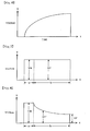
- the organic EL elements described above have diode characteristics including a predetermined electric capacitance (parasitic capacitance) from the laminated structure thereof. Then, when the organic EL elements are driven by constant currents, as described above, the waveform of the anode voltage of the elements has such a characteristic that it gently rises up as shown in Fig. 6 because the constant current circuits are high impedance output circuits in the operation principle thereof. That is, in Fig. 6, a vertical axis shows the anode voltage V of the element, and a lateral axis shows an elapsed time t.
- the rising-up curve of the anode voltage V is changed by various conditions such as the lighting/non-lighting condition of the elements when they were scanned last time, the lighting/non-lighting condition of adjacent elements, and the like. Then, the luminance of the organic EL elements is changed by the change of the rising-up curve. However, the substantial luminance of the display panel cannot help being dropped because the rising-up of the light emission of the element is delayed.
- Fig. 7 shows an anode voltage waveform when a precharge voltage (VM) is set equal to the forward direction voltage (VF) of an element.
- a vertical axis shows the anode voltage V of the element, and a lateral axis shows an elapsed time t also in Fig. 7.
- a period a shows a precharge period with respect to the element, and a period b shows the constant current drive period of the element.
- the precharge drive described above is executed as well as when the forward direction voltages VF of the EL elements are obtained by making use of, for example, the sampling/holding means and the control means described above is employed to control the value of the output voltage VH supplied from the drive voltage source 6. That is, when the light emission luminance of light-emitting elements is dropped while they are, for example, being lit, the forward direction voltages VF of the elements are dropped from the state shown in Fig. 7 to the state shown in Fig. 8.
- a final forward direction voltage VF cannot be sampled and held at the timing of a sampling operation but a voltage denoted by VF' is held based on the timing of the sampling operation, and the output voltage VH of the drive voltage source 6 is controlled based on the thus held voltage VF'.
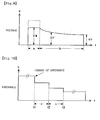
- a precharge voltage VM lower than that shown in Fig. 9 is created based on the held voltage VF' shown in Fig. 8. Accordingly, the luminance of the light-emitting elements does not drop instantly but drops stepwise as shown in Fig. 10. Thus, a problem is arisen in that the gentle change of luminance as described above is felt unnatural by a user.
- t1, t2, and t3 in Fig. 10 show timing at which sampling operations are executed, and c shows sampling intervals.
- the above problem is also arisen similarly when the luminance is risen. Further, it is also arisen when the light-emitting elements are driven by the constant currents without executing the above precharge. Furthermore, the above problem is not limited to the case in which the light emission luminance is changed while the display panel is being lit but a similar problem is also arisen when, for example, the display panel starts to be lit.
- the above phenomenon is caused by the timing of the sampling hold. Accordingly, it is conceived to execute the sampling hold at timing of short intervals. However, when the sampling hold is executed at the timing of the short intervals, a drive power necessary to the sampling hold operation and a held voltage are discharged each time the sampling hold operation is executed, thereby a power is wasted. Therefore, when for example, the drive method is used in mobile terminals, and the like, the power of batteries are wasted, and thus this drive method is not preferable.
- An object of the present invention which was made in view of the above technical views of point, is to provide a drive method of a light-emitting display panel capable of reducing the drive electric power as well as capable of improving the gentle operation characteristics of light emission luminance generated when, for example, the light emission luminance of the display panel is changed or when the display panel starts to be lit, as described above, and to provide an organic EL display device using the drive method.
- a drive method of a light-emitting display panel which was made to achieve the above object, is a drive method of a light-emitting display panel including light-emitting elements whose lighting is controlled through constant current circuits, wherein the drive method includes the steps of supplying constant currents to the light-emitting elements from the constant current circuits making use of the voltage output from a drive voltage source, controlling the voltage output from the drive voltage source based on the forward direction voltages of the light-emitting elements, and adjusting the timing at which the voltage output from the drive voltage source is controlled based on the lighting drive condition of the light-emitting elements.
- the voltage output from the drive voltage source based on the forward direction voltages be controlled at timing of shorter intervals. Further, it is preferable that the voltage output from the drive voltage source based on the forward direction voltages be controlled also at timing of shorter intervals when the light emission luminance of the light-emitting display panel is changed. In this case, when the light emission luminance of the light-emitting display panel is changed beyond a predetermined range set beforehand, the voltage output from the drive voltage source based on the forward direction voltages may be controlled at timing of shorter intervals.
- the voltage output from the drive voltage source based on the forward direction voltages may be controlled when the light-emitting display panel starts to be lit. Further, it is preferable that the voltage output from the drive voltage source based on the forward direction voltages be controlled also when the light emission luminance of the light-emitting display panel is changed.
- the voltage output from the drive voltage source based on the forward direction voltages be repeatedly controlled a plurality of times when the light-emitting display panel starts to be lit or when the light emission luminance of the light-emitting display panel is changed.
- the forward direction voltages may be sampled at the timing at which constant currents are supplied from the constant current circuits to the light-emitting elements, and the forward direction voltages may be obtained by a sampling/holding circuit for holding the sampled voltage values in a preferable embodiment. Further, the forward direction voltages may be obtained by adding a constant current to a dummy light-emitting element that does not contribute to the light emission of the light-emitting display panel.
- a voltage drop in the constant current circuits be controlled substantially constant by controlling the voltage output from the drive voltage source, and a voltage increasing type DC-DC converter is preferably used as the drive voltage source.
- organic EL elements are utilized as the light-emitting elements and driven and lit by employing the drive method described above.
- the forward direction voltages of the light-emitting elements supplied through the constant current circuits are detected so as to control the voltage output from the drive voltage source, thereby the constant current circuits for supplying constant currents to the respective EL elements can minimize the voltage drop thereof within a range in which a constant current supply operation can be secured. Accordingly, this arrangement can contribute to the reduction of an electric power loss in the constant current circuits.
- the voltage output from the drive voltage source is controlled at timing of shorter intervals than ordinary intervals when, for example, the light-emitting display panel starts to be lit or when the light emission luminance of the light-emitting display panel is changed, thereby the gentle changing characteristics of the light emission luminance of the display panel can be improved. Then, when the first control aspect is employed, the intervals at which the forward direction voltages of the elements are sampled and held are shortened for only a predetermined period, thereby the degree of an electric power loss caused by the sampling and holding operation can be reduced.
- the voltage output from the drive voltage source based on the forward direction voltages of the elements is controlled only when, for example, the light-emitting display panel starts to be lit or when the light emission luminance of the light-emitting display panel is changed.
- the gentle changing characteristics of the light emission luminance can be improved by repeatedly controlling the voltage output from the drive voltage source a plurality of times.
- the degree of an electric power loss caused by the sampling and holding operation can be more reduced.
- the voltage output from the drive voltage source is controlled only when the light-emitting display panel starts to be lit or when the light emission luminance of the light-emitting display panel is changed.
- the electric deterioration with age and temperature dependency of the light-emitting elements can be compensated at the time. Accordingly, sufficient compensation characteristics can be secured in practical use.
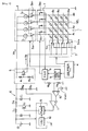
- FIG. 1 shows a passive matrix drive system to which the present invention is applied and an example of a display panel whose light emission is controlled by the passive matrix drive system.
- a display panel 1 an anode line drive circuit 2, a cathode line scan circuit 3, and a light emission control circuit 4 that drive the display panel 1, and further a reverse bias voltage creation circuit 5 have the same functions as those of the respective circuits shown in Fig. 5 described above, and thus the detailed description thereof is appropriately omitted.
- a sampling switch 7 is interposed between the anode line drive circuit 2 and the display panel 1.
- the sampling switch 7 includes switches denoted by Sh1 to Shn in correspondence to drive switches Sx1 to Sxn in the anode line drive circuit 2 and anode lines A1 to An in the display panel 1. These switches Sh1 to Shn are opened and closed in response to a control signal from a sampling/holding circuit 8.
- the light emission control circuit 4 drives the sampling/holding circuit 8 through a sampling timing control circuit 9 which will be described later in synchronism with that the light emission control circuit 4 lights and controls respective EL elements through the respective drive switches SX1 to SXn to thereby close the respective switches Sh1 to Shn. Then, the forward direction voltages VF of the respective EL elements are supplied to the sampling/holding circuit 8 through the respective switches Sh1 to Shn, thereby the forward direction voltages VF of the respective EL elements can be obtained.
- a forward direction voltage held by the sampling/ holding circuit 8 is supplied to one input terminal (inverted input terminal) of an error amplifier 10 through a voltage division circuit composed of resistors R5 and R6.
- a reference voltage Vref is supplied to the other input terminal (non-inverted input terminal) of the error amplifier 10, and thus a comparison output (error output) between the forward direction voltage and the reference voltage is created by the error amplifier 10.
- the output from the error amplifier 10 is supplied to one input terminal (non-inverted input terminal) of a differential amplifier 11. Further, the output from resistors R7 and R8 that divide the output voltage VH of a drive voltage source 6 is supplied to the other input terminal (inverted input terminal) of the differential amplifier 11. Therefore, the values of the output voltages of the differential amplifier 11 include both the output information of the forward direction voltages VF of the light-emitting elements and the output information of the output voltage VH of the drive voltage source 6.
- a voltage increasing type DC-DC converter is used as the drive voltage source 6, and the output from the differential amplifier 11 is supplied to a switching regulator circuit 14 constituting the DC-DC converter.
- the drive voltage source 6 composed of the DC-DC converter that will be described below creates a direct current output by pulse width modulation (PWM) control, it may utilize pulse frequency modulation (PFM) control.
- PWM pulse width modulation
- PFM pulse frequency modulation
- the switching regulator circuit 14 includes a PWM circuit 15 and a reference oscillator 16 disposed therein.
- the output from the differential amplifier 11 is supplied to the PWM circuit 15 and modulates the pulse width of the signal supplied from the reference oscillator 16 so that an npn transistor Q2 is switched in response to the modulated pulse output. That is, the electric power energy from a DC voltage source 12 is accumulated in an inductor L1 by the turning-on operation of the npn transistor Q2. In contrast, the electric power energy accumulated in the inductor L1 is accumulated in a capacitor C1 through a diode D3 by the turning-off operation of the npn transistor Q2.
- an increased DC output voltage can be obtained as the terminal voltage of the capacitor C1 by repeating the turning-on/off operation of the transistor Q2, and the DC output acts as the output voltage VH output from the drive voltage source 6. Accordingly, in this embodiment, the output voltage VH depends on the forward direction voltages VF when the EL elements are lit.
- the output voltage VH is controlled also by the output voltage divided by the resistors R7 and R8.
- the respective constant current circuits I1 to In of the anode line drive circuit 2 can be controlled to have a definite voltage drop value that permits the constant current circuits I1 to In to guarantee the constant current drive by appropriately selecting the voltage dividing ratio of the resistors R7 and R8. With this arrangement, the power loss in the respective constant current circuits I1 to In can be reduced as much as possible.
- sampling/holding circuit 8 executed by the above sampling timing control circuit 9 . That is, in the first control aspect, the sampling/holding circuit 8 is operated to select an ordinary sampling hold intervals and sampling hold intervals executed at timing shorter than that of the ordinary sampling hold intervals.
- the sampling timing control circuit 9 monitors the light emission state of the display panel 1 controlled by the light emission control circuit 4.
- the light emission control circuit 4 supplies an instruction signal to the sampling timing control circuit 9 when, for example, the light emission luminance of the light-emitting display panel is changed or when the light-emitting display panel starts to be lit.
- the sampling timing control circuit 9 controls the sampling/holding circuit 8 so that it executes a sampling hold operation at shorter intervals for a predetermined period.
- the sampling timing control circuit 9 instructs the sampling/holding circuit 8 to execute the sampling hold operation at timing of, for example, several hundreds of milliseconds, thereby the sampling/holding circuit 8 holds the forward direction voltages VF of the EL elements. Then, the DC-DC converter acting as the drive voltage source 6 controls the value of the output voltage VH based on the forward direction voltages VF of the EL elements.
- the sampling timing control circuit 9 instructs the sampling/holding circuit 8 to execute the sampling hold at timing of, for example, several tens of milliseconds for a predetermined period.
- Fig. 2 shows an example of control executed when the light emission luminance of the display panel is dropped. That is, when the display panel is ordinarily driven, the sampling/holding circuit 8 executes the sampling hold at sampling intervals (several hundreds of milliseconds) shown by c. Then, when the light emission luminance of the display panel is dropped (changed), the sampling/holding circuit 8 executes the sampling hold at sampling intervals (several tens of milliseconds) shown by c' for a predetermined period.
- the sampling/holding circuit 8 holds the forward direction voltages VF of the EL elements, and the DC-DC converter acting as the drive voltage source 6 controls the value of the output voltage VH based on the forward direction voltages VF of the EL elements. Since the output voltage VH is controlled at the sampling intervals shown by c' in this case, the luminance of the light-emitting elements drops stepwise as shown in Fig. 2. However, this drop of luminance is almost instantly executed as compared with the example shown in Fig. 10. Accordingly, a user does not visually have a feeling that the light emission luminance gently changes stepwise.
- Fig. 2 shows an example of control that is executed when the light emission luminance of the display panel is dropped
- the light emission luminance also can be risen almost instantly when the light emission luminance is risen.
- the value of the output voltage VH can be promptly risen similarly by controlling the value of the output voltage VH at the sampling intervals shown by c'.
- the user visually has a feeling as if the light emission luminance of the display device rises instantly.
- the voltage output from the drive voltage source based on the forward direction voltages is controlled at shorter timing.
- the voltage output from the drive voltage source may be controlled at shorter timing.
- the intervals, at which the forward direction voltages of the EL elements are subjected to the sampling hold are set shorter than those in the ordinary operation. As a result, the degree of electric power loss caused by the sampling hold operation can be reduced.
- the voltage output from the drive voltage source based on the forward direction voltages of the elements is controlled only when the light emission luminance of the light-emitting display panel is changed or only when the light-emitting display panel starts to be lit.
- the sampling timing control circuit 9 sends an instruction signal to the sampling/holding circuit 8, thereby the sampling/holding circuit 8 repeatedly executes the sampling operation at the short intervals c' of several tens of milliseconds described above for a predetermined period.
- the value of the output voltage VH is controlled at the sampling intervals shown by c', thereby the value of the output voltage VH can be risen promptly.
- the user visually has a feeling as if the light emission luminance of the display device rises instantly.
- the operation for sampling and holding the forward direction voltages of the elements is executed only when the light-emitting display panel starts to be lit or only when the light emission luminance of the light-emitting display panel is changed also in this case, a disadvantage that the electric power loss is caused by the sampling hold operation at all times can be avoided.
- the voltage output from the drive voltage source based on the forward direction voltages of the elements be controlled once only when the light emission luminance of the light-emitting display panel is changed or only when the light-emitting display panel starts to be lit.
- the sampling operation is executed in a predetermined period of time (for example, in several seconds) after the light emission luminance of the light-emitting display panel has been changed or after the light-emitting display panel has started to be lit.
- the forward direction voltages of the respective EL elements whose lighting is controlled by the constant current circuits I1 to In provided with the anode line drive circuit 2 are sampled and held as a means for obtaining the forward direction voltages VF of the EL elements as shown in Fig. 1.
- an arrangement shown in Fig. 4 may be preferably used as the means for obtaining the forward direction voltages VF of the EL elements.
- a dummy organic EL element Ex that does not contribute to light emission is formed as a film on the display panel 1 together with organic EL elements for display, and a constant current is supplied to the dummy organic EL element Ex through a constant current circuit 21 driven by the output voltage VH. Then, the anode terminal of the dummy organic EL element Ex is connected to the inverted input terminal of an operational amplifier 22 and the cathode terminal thereof is grounded as well as connected to the non-inverted input terminal of the operational amplifier 22.
- the operational amplifier 22 constitutes a negative feedback amplifier having a feedback resistor R9 connected between the output terminal of the operational amplifier 22 and the inverted input terminal thereof, and the output from the operational amplifier 22 is supplied to the sampling/holding circuit 8 shown in Fig. 1. According to this arrangement, the forward direction voltages VF of the EL elements can be obtained at all times making use of the dummy organic EL element Ex, thereby the switches Sh1 to Shn, and the like as shown in Fig. 1 can be omitted.
- the dummy organic EL element Ex is also lit.
- the present invention is by no means limited to the passive matrix drive system and also can be applied to an active matrix drive system.
- the display device making use of the drive method of the present invention in a case in which, for example, the light emission luminance of the light-emitting display panel is changed or in other case, since the output voltage from the drive voltage source is controlled at timing having intervals shorter than those in an ordinary state, the gentle changing characteristics of the light emission luminance of the display device can be improved.
Landscapes
- Engineering & Computer Science (AREA)
- Physics & Mathematics (AREA)
- Computer Hardware Design (AREA)
- General Physics & Mathematics (AREA)
- Theoretical Computer Science (AREA)
- Electroluminescent Light Sources (AREA)
- Control Of Indicators Other Than Cathode Ray Tubes (AREA)
- Control Of El Displays (AREA)
Abstract
Description
According to this arrangement, the forward direction voltages VF of the EL elements can be obtained at all times making use of the dummy organic EL element Ex, thereby the switches Sh1 to Shn, and the like as shown in Fig. 1 can be omitted.
Claims (25)
- A drive method of a light-emitting display panel including light-emitting elements whose lighting is controlled through constant current circuits, comprising the steps of:supplying constant currents to the light-emitting elements from the constant current circuits making use of the voltage output from a drive voltage source;controlling the voltage output from the drive voltage source based on the forward direction voltages of the light-emitting elements; andadjusting the timing at which the voltage output from the drive voltage source is controlled based on the lighting drive condition of the light-emitting elements.
- A drive method of a light-emitting display panel according to claim 1, wherein when the light-emitting display panel starts to be lit, the voltage output from the drive voltage source based on the forward direction voltages is controlled at timing of shorter intervals.
- A drive method of a light-emitting display panel according to claim 1, wherein when the light emission luminance of the light-emitting display panel is changed, the voltage output from the drive voltage source based on the forward direction voltages is controlled at timing of shorter intervals.
- A drive method of a light-emitting display panel according to claim 1, wherein when the light emission luminance of the light-emitting display panel is changed beyond a predetermined range set beforehand, the voltage output from the drive voltage source based on the forward direction voltages is controlled at timing of shorter intervals.
- A drive method of a light-emitting display panel according to claim 1, wherein the voltage output from the drive voltage source based on the forward direction voltages is controlled when the light-emitting display panel starts to be lit.
- A drive method of a light-emitting display panel according to claim 1, wherein the voltage output from the drive voltage source based on the forward direction voltages is controlled when the light emission luminance of the light-emitting display panel is changed.
- A drive method of a light-emitting display panel according to claim 5 or 6, wherein the voltage output from the drive voltage source based on the forward direction voltages is repeatedly controlled a plurality of times when the light-emitting display panel starts to be lit or when the light emission luminance of the light-emitting display panel is changed.
- A drive method of a light-emitting display panel according to any one of claims 1 to 6, wherein the forward direction voltages are sampled at the timing at which constant currents are supplied from the constant current circuits to the light-emitting elements, and the forward direction voltages are obtained by a sampling/holding circuit for holding the sampled voltage values.
- A drive method of a light-emitting display panel according to claim 7, wherein the forward direction voltages are sampled at the timing at which the constant currents are supplied from the constant current circuits to the light-emitting elements, and the forward direction voltages are obtained by a sampling/holding circuit for holding the sampled voltage values.
- A drive method of a light-emitting display panel according to any one of claims 1 to 6, wherein the forward direction voltages are obtained by adding a constant current to a dummy light-emitting element that does not contribute to the light emission of the light-emitting display panel.
- A drive method of a light-emitting display panel according to claim 7, wherein the forward direction voltages are obtained by adding a constant current to a dummy light-emitting element that does not contribute to the light emission of the light-emitting display panel.
- A drive method of a light-emitting display panel according to any one of claims 1 to 6, wherein a voltage drop in the constant current circuits is controlled substantially constant by controlling the voltage output from the drive voltage source.
- A drive method of a light-emitting display panel according to claim 7, wherein a voltage drop in the constant current circuits is controlled substantially constant by controlling the voltage output from the drive voltage source.
- A drive method of a light-emitting display panel according to any one of claims 1 to 6, wherein a voltage increasing type DC-DC converter is used as the drive voltage source.
- A drive method of a light-emitting display panel according to claim 7, wherein a voltage increasing type DC-DC converter is used as the drive voltage source.
- An organic EL display device, wherein the light-emitting elements are composed of organic EL elements driven and lit by a drive method according to any one of claims 1 to 6.
- An organic EL display device, wherein the light-emitting elements are composed of organic EL elements driven and lit by a drive method according to claim 7.
- An organic EL display device, wherein the light-emitting elements are composed of organic EL elements driven and lit by a drive method according to claim 8.
- An organic EL display device, wherein the light-emitting elements are composed of organic EL elements driven and lit by a drive method according to claim 9.
- An organic EL display device, wherein the light-emitting elements are composed of organic EL elements driven and lit by a drive method according to claim 10.
- An organic EL display device, wherein the light-emitting elements are composed of organic EL elements driven and lit by a drive method according to claim 11.
- An organic EL display device, wherein the light-emitting elements are composed of organic EL elements driven and lit by a drive method according to claim 12.
- An organic EL display device, wherein the light-emitting elements are composed of organic EL elements driven and lit by a drive method according to claim 13.
- An organic EL display device, wherein the light-emitting elements are composed of organic EL elements driven and lit by a drive method according to claim 14.
- An organic EL display device, wherein the light-emitting elements are composed of organic EL elements driven and lit by a drive method according to claim 15.
Applications Claiming Priority (2)
| Application Number | Priority Date | Filing Date | Title |
|---|---|---|---|
| JP2002009808 | 2002-01-18 | ||
| JP2002009808A JP3882995B2 (en) | 2002-01-18 | 2002-01-18 | Driving method of light emitting display panel and organic EL display device |
Publications (2)
| Publication Number | Publication Date |
|---|---|
| EP1329873A2 true EP1329873A2 (en) | 2003-07-23 |
| EP1329873A3 EP1329873A3 (en) | 2008-05-14 |
Family
ID=19191539
Family Applications (1)
| Application Number | Title | Priority Date | Filing Date |
|---|---|---|---|
| EP02024912A Withdrawn EP1329873A3 (en) | 2002-01-18 | 2002-11-06 | Drive method of light-emitting display panel and organic EL display device |
Country Status (4)
| Country | Link |
|---|---|
| US (1) | US7236148B2 (en) |
| EP (1) | EP1329873A3 (en) |
| JP (1) | JP3882995B2 (en) |
| CN (1) | CN100385477C (en) |
Cited By (1)
| Publication number | Priority date | Publication date | Assignee | Title |
|---|---|---|---|---|
| US8115758B2 (en) | 2004-11-24 | 2012-02-14 | Semiconductor Energy Laboratory Co., Ltd. | Light emitting device |
Families Citing this family (20)
| Publication number | Priority date | Publication date | Assignee | Title |
|---|---|---|---|---|
| JP3991003B2 (en) * | 2003-04-09 | 2007-10-17 | 松下電器産業株式会社 | Display device and source drive circuit |
| JP4536554B2 (en) * | 2004-03-30 | 2010-09-01 | ローム株式会社 | Electronics |
| JP4539963B2 (en) * | 2004-06-10 | 2010-09-08 | 東北パイオニア株式会社 | Active drive type light emitting display device and electronic device equipped with the display device |
| JP2006119274A (en) * | 2004-10-20 | 2006-05-11 | Nec Lighting Ltd | Led display device and display control method |
| FR2879007A1 (en) * | 2004-12-06 | 2006-06-09 | St Microelectronics Sa | AUTOMATIC ADAPTATION OF THE PRELOADING VOLTAGE OF AN ELECTROLUMINESCENT SCREEN |
| JP2006343531A (en) * | 2005-06-09 | 2006-12-21 | Tohoku Pioneer Corp | Driving device and driving method of light emitting panel |
| JP2007003954A (en) * | 2005-06-24 | 2007-01-11 | Rohm Co Ltd | Display control circuit, display device, and semiconductor integrated circuit |
| JP2007114308A (en) * | 2005-10-18 | 2007-05-10 | Tohoku Pioneer Corp | Driving unit and driving method for light emitting display panel |
| US7872430B2 (en) | 2005-11-18 | 2011-01-18 | Cree, Inc. | Solid state lighting panels with variable voltage boost current sources |
| US20080032758A1 (en) * | 2006-08-02 | 2008-02-07 | Ramin Rostami | Handheld device protective case |
| US7944420B2 (en) * | 2007-09-28 | 2011-05-17 | Osram Sylvania Inc. | Light emitting diode driver providing current and power control |
| US9165493B2 (en) * | 2008-10-14 | 2015-10-20 | Apple Inc. | Color correction of electronic displays utilizing gain control |
| JP2010160369A (en) * | 2009-01-09 | 2010-07-22 | Nippon Seiki Co Ltd | Organic el display device |
| WO2011145448A1 (en) * | 2010-05-17 | 2011-11-24 | Necライティング株式会社 | Illumination device and light-adjusting method |
| JP2012047807A (en) | 2010-08-24 | 2012-03-08 | Sony Corp | Display device and electronic equipment |
| JP5684524B2 (en) * | 2010-09-29 | 2015-03-11 | トッパン・フォームズ株式会社 | Luminescent display medium |
| KR102738534B1 (en) | 2020-07-21 | 2024-12-06 | 주식회사 엘엑스세미콘 | Led driver and led driving method |
| CN112037725B (en) * | 2020-08-28 | 2023-01-10 | 青岛信芯微电子科技股份有限公司 | Display device and display method |
| CN113223449B (en) * | 2021-05-08 | 2022-09-02 | 厦门寒烁微电子有限公司 | Driving circuit of LED display and capacitance compensation method |
| CN114694593B (en) * | 2022-03-31 | 2023-07-28 | 武汉天马微电子有限公司 | Pixel driving circuit, driving method thereof, display panel and display device |
Family Cites Families (11)
| Publication number | Priority date | Publication date | Assignee | Title |
|---|---|---|---|---|
| US3708717A (en) * | 1969-05-16 | 1973-01-02 | Energy Conversion Devices Inc | Electroluminescent array and method and apparatus for controlling discrete points on the array |
| JPS60255054A (en) * | 1984-05-28 | 1985-12-16 | Hitachi Ltd | Applied voltage detection device for power converter |
| US4707692A (en) * | 1984-11-30 | 1987-11-17 | Hewlett-Packard Company | Electroluminescent display drive system |
| JPH05265399A (en) * | 1992-03-23 | 1993-10-15 | Toshiba Corp | Display device |
| US5457488A (en) * | 1993-04-12 | 1995-10-10 | Oki Electric Industry Co., Ltd. | Method and apparatus for controlling array of light-emitting elements |
| JP3313830B2 (en) | 1993-07-19 | 2002-08-12 | パイオニア株式会社 | Display device drive circuit |
| US5594463A (en) * | 1993-07-19 | 1997-01-14 | Pioneer Electronic Corporation | Driving circuit for display apparatus, and method of driving display apparatus |
| JP2001143867A (en) * | 1999-11-18 | 2001-05-25 | Nec Corp | Organic EL drive circuit |
| JP2001195026A (en) * | 2000-01-14 | 2001-07-19 | Victor Co Of Japan Ltd | Matrix type display device |
| JP2001223074A (en) * | 2000-02-07 | 2001-08-17 | Futaba Corp | Organic electroluminescence device and driving method thereof |
| US6590343B2 (en) * | 2000-06-06 | 2003-07-08 | 911Ep, Inc. | LED compensation circuit |
-
2002
- 2002-01-18 JP JP2002009808A patent/JP3882995B2/en not_active Expired - Fee Related
- 2002-09-26 US US10/255,179 patent/US7236148B2/en not_active Expired - Fee Related
- 2002-11-06 EP EP02024912A patent/EP1329873A3/en not_active Withdrawn
-
2003
- 2003-01-20 CN CNB031018548A patent/CN100385477C/en not_active Expired - Fee Related
Cited By (2)
| Publication number | Priority date | Publication date | Assignee | Title |
|---|---|---|---|---|
| US8115758B2 (en) | 2004-11-24 | 2012-02-14 | Semiconductor Energy Laboratory Co., Ltd. | Light emitting device |
| US8605076B2 (en) | 2004-11-24 | 2013-12-10 | Semiconductor Energy Laboratory Co., Ltd. | Light emitting device |
Also Published As
| Publication number | Publication date |
|---|---|
| US20030137475A1 (en) | 2003-07-24 |
| CN1432981A (en) | 2003-07-30 |
| JP3882995B2 (en) | 2007-02-21 |
| US7236148B2 (en) | 2007-06-26 |
| JP2003216105A (en) | 2003-07-30 |
| CN100385477C (en) | 2008-04-30 |
| EP1329873A3 (en) | 2008-05-14 |
Similar Documents
| Publication | Publication Date | Title |
|---|---|---|
| US7088319B2 (en) | Drive method of light-emitting display panel and organic EL display device | |
| US7236148B2 (en) | Drive method of light-emitting display panel and organic EL display device | |
| US6894436B2 (en) | Drive method of light-emitting display panel and organic EL display device | |
| EP1291838B1 (en) | Apparatus and method for driving luminescent display panel | |
| EP1486943A2 (en) | Drive device and drive method for light emitting display panel | |
| JP4822387B2 (en) | Drive device for organic EL panel | |
| US6587087B1 (en) | Capacitive light-emitting element display device and driving method therefor | |
| JP3613451B2 (en) | Driving device and driving method for multicolor light emitting display panel | |
| KR100795459B1 (en) | Active matrix electroluminescent display devices | |
| US7471288B2 (en) | Light emitting display device and driving control method therefor | |
| JP3620985B2 (en) | Capacitive light emitting device display device and driving method thereof | |
| US20050052448A1 (en) | Drive device and drive method of light emitting display panel | |
| KR101633426B1 (en) | Power supplying apparatus of Organic Light Emitting Display | |
| JP3773185B2 (en) | Driving device and driving method of light emitting display panel | |
| JP4878414B2 (en) | Capacitive light emitting display panel drive device | |
| JP2002366101A (en) | Light emitting display panel driving device | |
| KR20200070820A (en) | Display Device | |
| JP3773181B2 (en) | Driving device for light emitting display panel | |
| JP3646916B2 (en) | Multicolor light emitting display panel drive device | |
| US20090184900A1 (en) | Image display device and display device control method | |
| CN218547961U (en) | TFT pixel circuit capable of stably controlling current and display device | |
| JP2005003837A (en) | Driving device of light emitting display panel and driving method |
Legal Events
| Date | Code | Title | Description |
|---|---|---|---|
| PUAI | Public reference made under article 153(3) epc to a published international application that has entered the european phase |
Free format text: ORIGINAL CODE: 0009012 |
|
| AK | Designated contracting states |
Designated state(s): AT BE BG CH CY CZ DE DK EE ES FI FR GB GR IE IT LI LU MC NL PT SE SK TR |
|
| AX | Request for extension of the european patent |
Extension state: AL LT LV MK RO SI |
|
| RTI1 | Title (correction) |
Free format text: DRIVE METHOD OF LIGHT-EMITTING DISPLAY PANEL AND ORGANIC EL DISPLAY DEVICE |
|
| PUAL | Search report despatched |
Free format text: ORIGINAL CODE: 0009013 |
|
| AK | Designated contracting states |
Kind code of ref document: A3 Designated state(s): AT BE BG CH CY CZ DE DK EE ES FI FR GB GR IE IT LI LU MC NL PT SE SK TR |
|
| AX | Request for extension of the european patent |
Extension state: AL LT LV MK RO SI |
|
| 17P | Request for examination filed |
Effective date: 20081107 |
|
| AKX | Designation fees paid |
Designated state(s): DE FR GB |
|
| 17Q | First examination report despatched |
Effective date: 20101124 |
|
| STAA | Information on the status of an ep patent application or granted ep patent |
Free format text: STATUS: THE APPLICATION IS DEEMED TO BE WITHDRAWN |
|
| 18D | Application deemed to be withdrawn |
Effective date: 20110405 |