EP1329803A2 - Conditional sum adder - Google Patents
Conditional sum adder Download PDFInfo
- Publication number
- EP1329803A2 EP1329803A2 EP02254426A EP02254426A EP1329803A2 EP 1329803 A2 EP1329803 A2 EP 1329803A2 EP 02254426 A EP02254426 A EP 02254426A EP 02254426 A EP02254426 A EP 02254426A EP 1329803 A2 EP1329803 A2 EP 1329803A2
- Authority
- EP
- European Patent Office
- Prior art keywords
- input
- carry
- data
- result
- unit
- Prior art date
- Legal status (The legal status is an assumption and is not a legal conclusion. Google has not performed a legal analysis and makes no representation as to the accuracy of the status listed.)
- Withdrawn
Links
Images




Classifications
-
- G—PHYSICS
- G06—COMPUTING OR CALCULATING; COUNTING
- G06F—ELECTRIC DIGITAL DATA PROCESSING
- G06F7/00—Methods or arrangements for processing data by operating upon the order or content of the data handled
- G06F7/38—Methods or arrangements for performing computations using exclusively denominational number representation, e.g. using binary, ternary, decimal representation
- G06F7/48—Methods or arrangements for performing computations using exclusively denominational number representation, e.g. using binary, ternary, decimal representation using non-contact-making devices, e.g. tube, solid state device; using unspecified devices
- G06F7/50—Adding; Subtracting
-
- G—PHYSICS
- G06—COMPUTING OR CALCULATING; COUNTING
- G06F—ELECTRIC DIGITAL DATA PROCESSING
- G06F7/00—Methods or arrangements for processing data by operating upon the order or content of the data handled
- G06F7/38—Methods or arrangements for performing computations using exclusively denominational number representation, e.g. using binary, ternary, decimal representation
- G06F7/48—Methods or arrangements for performing computations using exclusively denominational number representation, e.g. using binary, ternary, decimal representation using non-contact-making devices, e.g. tube, solid state device; using unspecified devices
- G06F7/50—Adding; Subtracting
- G06F7/505—Adding; Subtracting in bit-parallel fashion, i.e. having a different digit-handling circuit for each denomination
- G06F7/506—Adding; Subtracting in bit-parallel fashion, i.e. having a different digit-handling circuit for each denomination with simultaneous carry generation for, or propagation over, two or more stages
- G06F7/507—Adding; Subtracting in bit-parallel fashion, i.e. having a different digit-handling circuit for each denomination with simultaneous carry generation for, or propagation over, two or more stages using selection between two conditionally calculated carry or sum values
-
- G—PHYSICS
- G06—COMPUTING OR CALCULATING; COUNTING
- G06F—ELECTRIC DIGITAL DATA PROCESSING
- G06F7/00—Methods or arrangements for processing data by operating upon the order or content of the data handled
- G06F7/38—Methods or arrangements for performing computations using exclusively denominational number representation, e.g. using binary, ternary, decimal representation
- G06F7/48—Methods or arrangements for performing computations using exclusively denominational number representation, e.g. using binary, ternary, decimal representation using non-contact-making devices, e.g. tube, solid state device; using unspecified devices
- G06F7/50—Adding; Subtracting
- G06F7/501—Half or full adders, i.e. basic adder cells for one denomination
- G06F7/503—Half or full adders, i.e. basic adder cells for one denomination using carry switching, i.e. the incoming carry being connected directly, or only via an inverter, to the carry output under control of a carry propagate signal
-
- G—PHYSICS
- G06—COMPUTING OR CALCULATING; COUNTING
- G06F—ELECTRIC DIGITAL DATA PROCESSING
- G06F2207/00—Indexing scheme relating to methods or arrangements for processing data by operating upon the order or content of the data handled
- G06F2207/38—Indexing scheme relating to groups G06F7/38 - G06F7/575
- G06F2207/48—Indexing scheme relating to groups G06F7/48 - G06F7/575
- G06F2207/4802—Special implementations
- G06F2207/4812—Multiplexers
Definitions
- the present invention relates to a carry generator comprising an AND-gate for ANDing first and second input bits, an XOR-gate for XORing said first and second input bits and an input for receiving a carry propagation signal.
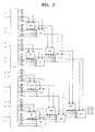
- Figure 1 is a schematic diagram of a prior art 64-bit conditional select adder 100.
- conditional select adder 100 has a plurality of conditional selection addition modules 110 through 180, each of which generates a carry by analyzing input values to be added and calculates a sum according to the presence of the carry, and a block carry generating block 190 which, in response to the carries generated by the conditional select addition modules, determines the presence of the carry and feeds the result back to the conditional selection addition module.
- Each of the conditional select addition modules 110 through 180 has a pre-carry-sum generating block 112 which analyzes input values to be added_and generates appropriate values in advance, a sum generating block 114 which obtains the limit of the value generated by the pre-carry-sum generating block 112, but obtains a sum in each case according to the presence of a carry, and a carry generating block 116 which generates a carry in response to the value generated by the pre-carry-sum generating block 112.
- the pre-carry-sum generating block 112 of the first conditional select addition module 110 analyzes input values to be added in the first conditional select addition module 110, and adds an appropriate value in advance.
- the sum generating block 114 generates a sum when there is a carry and a sum when there is no carry, and the carry generating block 116 outputs the carry of the first conditional select addition module 110 to the block carry generating block 190.
- the pre-carry-sum generating blocks of the remaining conditional select addition modules 120 through 180 analyze input values to be added and perform addition with appropriate values in advance.
- the sum generating block generates a sum when there is a carry and a sum when there is no carry, and the carry generating block outputs the carry of each conditional select addition module to the block carry generating block 190.
- the block carry generating block 190 receives carries from 8-bit conditional select addition modules 110 through 180 and feeds the presence of a carry to the conditional select addition module of the next stage. As a result, the appropriate sum, according to the presence of a carry, is selected from among the sums which are calculated in advance in the sum generating block of each of the 8-bit conditional select addition modules 110 through 180
- Figure 2 is a block diagram of the sum generating block 114 of the 8-bit conditional select adder module shown in Figure 1.
- the sum generating block 114 shown in Figure 2 is formed basically with multiplexers using pass transistor logic (PTL) based on an NMOS transistor, and uses level restore blocks (LRBs) appropriate to the driving capability of a multiplexer for low power consumption and high speed operation.
- PTL pass transistor logic
- L level restore blocks
- M denotes a multiplexer
- S denotes single
- D denotes double
- L denotes a level restore block.
- MS means a single multiplexer
- MDL means a double multiplexer having a level restore block.
- Figure 3 is a block diagram of a carry generating block of the 8-bit conditional select adder module as shown in Figure 1
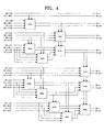
- Figure 4 is a block diagram of a block carry generating block as shown in Figure 1.
- the wiring is complicated in order to calculate a carry and a sum, and physical wire delay increases the overall delay time.
- PTL since PTL is used, an inverted signal is always needed, which increases wiring and power consumption.
- the block carries BC0, BC1, BC2, BC3, BC4, BC5, BC6, and BC7, generated in the block carry generating block 190 shown in Figure 4, are not output in synchronism, and therefore the generation of sums in the respective modules are also not synchronized.
- a carry generator according to the present invention is characterised by a multiplexer controlled by the output of the XOR-gate to select between the output of the AND-gate and a signal received at said input for receiving a carry propagation signal to provide a further carry propagations signal.
- the output of the AND-gate is selected when the output of the XOR-gate is 0.
- a carry generator according to the present invention may be included in an adder.
- Such an adder may also comprise first, second, third and fourth inputs for first and second adjacent bits of first and second multi-bit binary values and an OR-gate for ORing signals at the first and second inputs to produce a carry propagation signal and have the output of the OR-gate connected to said input for receiving a carry propagation signal and the third and fourth inputs provide the inputs to said AND-gate.
- a further AND-gate for ANDing the signals at the first and second inputs to produce a carry generating signal
- gate means for producing a signal which is the inverse of the output of the XOR-gate
- a further multiplexer controlled by the output of gate means to select between the outputs of the AND-gates to provide a carry generating signal
- a conditional select adder 600 has a plurality of conditional select addition modules 610, ..., 680 which analyze input values to be added and generate a sum according to the presence of a carry, and a block carry generating block 690 which, in response to the carries generated in the conditional select addition modules, determines the presence of a carry and feeds the result to the next stage conditional select addition module.
- the conditional select addition modules 610, ..., 680 each have a pre-carry-sum generating block 612, which analyzes input values to be added and generates an appropriate value in advance, a sum generating block 614 which generates the sum from a value generated by the pre-carry-sum generating block 612 according to the presence of a carry, and a carry generating block 616 which generates a carry in response to a value generated by the pre-carry-sum generating block 612.
- the pre-carry-sum generating block 612 of the first conditional select addition module 610 analyzes input values to be added in the first conditional select addition module.
- the sum generating block 614 generates sums for the cases where there is a carry and a where there is no carry, and the carry generating block 616 outputs the carry of the first conditional select addition module 610 to the block carry generating block 690.
- the carry generating block 616 receives XNOR value SH, XOR value SL, OR value CP and AND value CG derived from the input data X n and Y n , calculates a carry propagation value CP 0 and a carry generation value CG 0 using the received values, and outputs the calculated values to the block carry generating block 690.
- the carry generating block 616 generates carry propagation value C0P and carry generation value C0G from the input data X 0 and Y 0 , and outputs the generated values to CMOS multiplexers (MUX) for calculating carry propagation value C1P and carry generation value C1G of the next input data X 1 and Y 1 , and the sum generating block (SGB) 614.
- MUX CMOS multiplexers
- Each of the multiplexers in the present embodiment has a selection unit, a first input unit and a second input unit. If the value of a select signal input to the selection unit is '0', the signal input to the first input unit is selected and output, and if the value of the select signal is '1', the signal input to the second input unit is selected and output.
- the carry generation value C0G which is generated in the above step is input to the first input unit of the MUX 811a, which functions as a sub-carry generating unit for outputting a carry generation value, in order to calculate carry generation value C1G, and the result of performing an OR operation on input data X 1 and Y 1 is input to the second input unit of the MUX 811a.
- the result of performing an XNOR operation on the input data X 1 and Y 1 is input to the selection unit of the MUX 811a, and according to the XNOR result input, either the carry generation value C0G input to the first input unit or the result of performing an OR operation on input data X 1 and Y 1 input to the second input unit is selectively output.
- the carry generation value C0G input to the first input unit is output
- the result of performing an XNOR operation on input data X 1 and Y 1 is '1'
- the result of performing an OR operation on input data X 1 and Y 1 input to the second input unit is output.
- the output value of the MUX 811a is output as the C1G value which is the carry propagation value of input data X 1 and Y 1 , to the sum generating block 614, and used in calculating the sum of input data X 1 and Y 1 .
- the output is either input data X 1 and Y 1 , or the result of performing an OR operation on input data X 1 and Y 1 .
- the generated carry propagation value C0P is input to the second input unit of the MUX 811b which functions as a sub-carry generating unit for outputting a carry propagation value as shown in Figure 8, in order to calculate carry propagation value C1P, and the result of performing an AND operation on input data X 1 and Y 1 is input to the first input unit of the MUX 811b.
- the result of performing an XOR operation on input data X 1 and Y 1 is input to the selection unit of the MUX 811b, and according to the XOR result input, either the result of performing an OR operation on input data X 1 and Y 1 or the carry propagation value C0P is selectively output.
- the result of performing an XOR operation on input data X 1 and Y 1 is '0'
- the result of performing an AND operation on input data X 1 and Y 1 input to the first input unit is selected and output
- the carry propagation value C0P input to the second input unit is selected and output.
- the output value of the MUX 811b is output as C1P, which is the carry propagation value of input data X 1 and Y 1 , to the sum generating block 614, and is used in calculating the sum of input data X 1 and Y 1 .
- the output is either input data X 1 and Y 1 , or the result of performing an OR operation on input data X 1 and Y 1 .
- carry propagation value CP and carry generation value CG of input data X 2 and Y 2 generated in the pre-carry-sum generating block 612 are output to the MUXs 812a and 812b for calculating carry propagation C3P and carry generation C3G of next input data X 3 , and Y 3 .
- the carry generation value CG generated in the above step is input to the first input unit of the MUX 812a, and the result of performing an OR operation on input data X 3 and Y 3 is input to the second input unit of the MUX 812a.
- the result of performing an XNOR operation on input data X 3 and Y 3 is input to the selection unit of the MUX 812, and according to the input XNOR value, either the carry generation value input to the first input unit or the result of performing an AND operation on input data X 3 and Y 3 input to the second input unit is selectively output.
- the generated carry propagation value CP of X 2 and Y 2 is input to the second input unit of the MUX 812b, and the result of performing an AND operation on input data X 1 and Y 1 is also input to the first input unit of the MUX 812b.
- the result of performing an XOR operation on input data X 3 and Y 3 is input to the selection unit of the MUX 812b, and according to the input XNOR value, either the result of performing an AND operation on input data X 3 and Y 3 input to the first input unit, or the carry propagation value of X 2 and Y 2 input to the second input unit, is selectively output.
- the output is either input data X 3 and Y 3 , or the result of performing an OR operation on input data X 3 and Y 3 .
- the carry generation value C1G output from the MUX 811a is input as a selection signal for generating carry generation value C3G, to the selection unit of MUX 813b.
- the output of the MUX 812a and the output of the MUX 812b are respectively input to the two input units of the MUX 813b.
- the MUX 813b selects the signal which is output from the MUX 812a and input to the first input unit, and outputs the selected signal as carry generation value C3G for input signals X 2 , Y 2 , X 3 , and Y 3 .
- the MUX 813b selects the signal which is output from the MUX 812b and input to the second input unit, and outputs the selected signal as carry generation value C3G for input signals X 2 , Y 2 , X 3 , and Y 3 .
- the output carry generation value C3G is output to the sum generating block 614 and the MUX 815b.
- the carry generation value C1P output from the MUX 811b is input as a selection signal to the selection unit of the MUX 813a for generating carry propagation value C3P.
- the output of the MUX 812a and the output of the MUX 812b are respectively input to the two input units of the MUX 813a.
- the MUX 813a selects the signal which is output from the MUX 812a and input to the first input unit, and outputs the selected signal as carry propagation value C3G for input signals X 2 , Y 2 , X 3 , and Y 3 .
- the MUX 813b selects the signal which is output from the MUX 812b, and outputs the selected signal as carry propagation value C3G for input signals X 2 , Y 2 , X 3 , and Y 3 .
- the output carry generation value C3G is sent to the sum generating block 614 and MUX 815b.
- generated carry propagation value C3P and carry generation value C3G are output to the MUXs 815a and 815b for calculating carry propagation C5P and carry generation C5G of the next input data X 4 , Y 4 , X 5 , and Y 5 , and the sum generating block 614.
- the calculated carry propagation C3P and carry generation C3G are output to the MUXs 818a and 818b for calculating the carry propagation value CP and carry generation value CG of the carry generating block, and the calculated CP and CG are output to the block carry generating block 690.
- MUXs 814a through 818b perform the same functions as MUXs 811a, 811b, 812a, 812b, 813a and 813b.
- the carry generating block 616 uses no NAND or NOR gates, only XOR and XNOR gates, and calculates a carry using fewer gates and less internal wiring compared to the prior art, with reduced delay time, chip area, and power consumption.
- the basic operation of the sum generating block 614 is described by Table 2.
- the sum generating block 614 receives XNOR value SH, XOR value SL, OR value CP, and AND value CG of data X n and Y n , and carry propagation values (C0P, C1P, C2P, and C3P) and carry generation values (C0G, C1G, C2G, and C3G) from the carry generating block 616, and outputs a sum according to the Table 2.
- sum S n is the result of performing an XOR operation on input data X n and Y n
- sum S n is the result of performing an XNOR operation on input data X n and Y n .
- the sum generating block 614 receives XNOR value SH, XOR value SL, OR value CP, and AND value CG of data X n and Y n , input from the pre-carry-sum block 612, and carry propagation values (C0P, C1P, C3P, C5P) and carry generation values (C0G, C1G, C3G, C5G) input from the carry generating block 616, and based on the received values, obtains a sum in each of two cases according to the presence of a carry of two data X n (X 0 , X 1 , X 2 , X 3 , X 4 , X 5 , X 6 , X 7 ) and Y n (Y 0 , Y 1 , Y 2 , Y 3 , Y 4 , Y 5 , Y 6 , Y 7 ).
- sum Sn (S 0 , S 1 , S 2 , S 3 , S 4 , S 5 , S 6 , S 7 ) of each case is output by a MUX in the sum selection unit 1010 of the sum generating block 614 shown in Figure 9,
- the XOR value SL and XNOR value SH of input data X 0 and Y 0 are input respectively to MUXs of the sum selection block 1010, and are selectively output according to the value of carry input signal Cin input to the sum selection block 920.
- the carry input signal Cin is '0'
- the XOR value SL of the input data X 0 and Y 0 is selected
- the carry input signal Cin is '1'
- the XNOR value SH of the input data X 0 and Y 0 is selected. Then the selected value is output as sum S 0 of the input data X 0 and Y 0 .
- sum S1 of input data X 1 and Y 1 is calculated according to the following method.
- the XOR value SL and XNOR value SH of input data X 1 and Y 1 are input respectively to the two input units of MUX 910a.
- Carry propagation value C0P which functions as a selection signal and is generated in the carry generation block 616, is input to the selection unit of the MUX 910a. According to the input carry propagation value C0P, either the input XOR value SL or XNOR value SH of the input data X 1 and Y 1 is selectively output.
- the XOR value SL of the input data X 1 and Y 1 is selected, and when the input carry propagation value C0P is '1', the XNOR value SH of the input data X 1 and Y 1 is selected, and the selected value is output to the sum selection unit 1010.
- the XOR value SL and XNOR value SH of input data X 1 and Y 1 are input respectively to the two input units of the MUX 910b.
- Carry generation value C0G which functions as a selection signal, and is generated in the carry generation block 616, is input to the selection unit of the MUX 910b. According to the input carry generation value C0G, either the input XOR value SL or XNOR value SH of input data X 1 and Y 1 is selectively output.
- the XOR value SL of the input data X 1 and Y 1 is selected, and when the input carry generation value C0G is '1', the XNOR value SH of the input data X 1 and Y 1 is selected, and the selected value is output to the sum selection unit 1010.
- the outputs of the MUXs 910a and 910b are input to the sum selection unit 1010.
- One of the input values from the MUXs 910a and 910b is selected and output as sum S 1 of the input data X 1 and Y 1 , according to the carry input signal Cin value, in the same manner as calculating the sum of input data X 0 and Y 0 described above.
- the carry input signal Cin is '0'
- the input value from the MUX 910a is selected
- the carry input signal Cin is '1'
- the input value from the MUX 910b is selected, and the selected value is output as the sum S 1 .
- sum S 2 of the input data X 2 and Y 2 is calculated according to the following method.
- the XOR value SL and XNOR value SH of input data X 2 and Y 2 are input respectively to the two input units of MUX 911a.
- Carry propagation value C1P which functions as a selection signal, and is generated in the carry generation block 616, is input to the selection unit of the MUX 911a. According to the input carry propagation value C1P, either the input XOR value SL or XNOR value SH of input data X 2 and Y 2 is selectively output.
- the XOR value SL of the input data X 2 and Y 2 is selected, and when the input carry propagation value C1P is '1', the XNOR value SH of the input data X 2 and Y 2 is selected, and the selected value is output to the sum selection unit 1010.
- the XOR value SL and XNOR value SH of input data X 2 and Y 2 are input respectively to the two input units of the MUX 910b.
- Carry generation value C1G which functions as a selection signal, and is generated in the carry generation block 616, is input to the selection unit of the MUX 910b. According to the input carry generation value C1G, either the input XOR value SL or XNOR value SH of input data X 2 and Y 2 is selectively output.
- the XOR value SL of the input data X 1 and Y 1 is selected, and when the input carry generation value C1G is '1', the XNOR value SH of the input data X 1 and Y 1 is selected, and the selected value is output to the sum selection unit 1010.
- the outputs of the MUXs 911a and 911b are input to the sum selection unit 1010.
- One of the input values from the MUXs 910a and 910b is selected and output as sum S 2 of the input data X 2 and Y 2 , according to the carry input signal Cin value, in the same manner as calculating the sum of input data X 1 and Y 1 described above.
- the carry input signal Cin is '0'
- the input value from the MUX 911a is selected
- the carry input signal Cin is '1'
- the input value from the MUX 911b is selected, and the selected value is output as the sum S 2 .
- sum S 3 of the input data X 3 and Y 3 is calculated according to the following method.
- the XOR value SL and XNOR value SH of input data X 3 and Y 3 are input respectively to the two input units of MUX 912a.
- Carry propagation value CP of input data X 2 and Y 2 which functions as a selection signal, is input to the selection unit of the MUX 912a.
- the input carry propagation value CP either the input XOR value SL of input data X 3 and Y 3 , input to the first input unit, or XNOR value SH of input data X 3 and Y 3 , input to the second input unit, is selectively output.
- the XOR value SL of the input data X 3 and Y 3 input to the first input unit is selected, and when the input carry propagation value CP is '1', the XNOR value SH of the input data X 3 and Y 3 input to the second input unit is selected, and the selected value is output to the input units of the MUXs 913a and 913b.
- the XOR value SL and XNOR value SH of input data X 3 and Y 3 are input respectively to the two input units of the MUX 912b.
- Carry generation value CG of input data X 2 and Y 2 which functions as a selection signal, is input, to the selection unit of the MUX 912b.
- the input carry generation value CG either the input XOR value SL of input data X 3 and Y 3 , input to the first input unit, or XNOR value SH of input data X 3 and Y 3 , input to the second input unit, is selectively output.
- the XOR value SL of the input data X 3 and Y 3 is selected, and when the input carry generation value CG is '1', the XNOR value SH of the input data X 3 and Y 3 is selected, and the selected value is output to the MUXs 913a and 913b.
- the output values of the MUXs 912a and 912b are input respectively to the two input units of the MUX 913a, and C1P generated in the carry generating block 616 is input to the selection unit of the MUX 913a.
- the input carry propagation value C1P one of the input values from the MUXs 912a and 912b is selectively output.
- the input carry propagation value C1P is '0'
- the input value from the MUX 912b is selected
- the input carry propagation value C1P is '1'
- the input value from the MUX 912a is selected, and the selected value is output to the sum selection unit 1010.
- the output values of the MUXs 912a and 912b are input respectively to the two input units of the MUX 913b, and C1G generated in the carry generating block 616 is input to the selection unit of the MUX 913b.
- the input carry generation value C1G one of the input values from the MUXs 912a and 912b is selectively output.
- the input carry generation value C1G is '0'
- the input value from the MUX 912b is selected
- the input carry propagation value C1P is '1'
- the input value from the MUX 912a is selected, and the selected value is output to the sum selection unit 1010.
- the sum selection unit 1010 according to the carry input signal Cin value, one of the input values from the MUXs 913a and 913b is selected and output as sum S 3 of the input data X 3 and Y 3 , in the same manner as calculating the sum of input data X 2 and Y 2 described above
- the carry input signal Cin is '0'
- the input value from the MUX 913a is selected
- the carry input signal Cin is '1'
- the input value from the MUX 913b is selected, and the selected value is output as the sum S 3 of the input data X 3 and Y 3 .
- the sums of input data X 4 , Y 4 , X 5 , Y 5 , X 6 , Y 6 , X 7 , and Y 7 are calculated in the same manner as calculating the sums of X 2 , Y 2 , X 3 , and Y 3 described above.
- the sum generating block 614 does not use NAND or NOR gates, and therefore needs less internal wiring. Accordingly, delay time, chip area, and power consumption are less. Also, by using carry propagation values (C0P, C1P, C3P, C5P) and carry generation values (C0G, C1G, C3G, C5G) input from the carry generating block 616, the sum generating block 614 removes need for separate carry generating logic, simplifying wiring and logic.
- the carry generating block 616 and sum generating block 614 according to the present invention need only XNOR value SH, XOR value SL, OR value CP, and AND value CG of two input data X n and Y n from the pre-carry-sum generating block 612
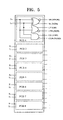
- the pre-carry-sum generating block 612 according to the present invention has needs only logic for XNOR, XOR, OR, and AND operations, unlike the prior art pre-carry-sum generating block 112 shown in Figure 5. Therefore, the conditional select adder according to the present invention has less fan-out than the prior art adder, and does not need NAND or NOR gates, reducing internal wiring, chip area, and power consumption.
- the result of performing an OR operation on input data X 0 and Y 0 , '1', and the result of performing an AND operation on input data X 0 and Y 0 , '1' are output as signal CP and signal CG, respectively, and are input as signal C0P to MUX 910a and signal C0G to MUX 910b, respectively, of the sum generating block 614 shown in Figure 9.
- the result of performing an AND operation on X 0 and Y 0 , '1' is input as an initial carry value to the first input unit of MUX 811a, and the result of performing an AND operation on X 1 and Y 1 , '0', is input to the second input unit.
- the result of performing an XNOR operation on X 1 and Y 1 , '1' is input to the selection unit of the MUX 811a, and according to this, the result of performing an AND operation on X 1 and Y 1 which is input to the second input unit, '0', is selected and output as signal C1G to the sum generating block 614.
- the result of performing an AND operation on X 1 and Y 1 , '0' is input to the first input unit of MUX 811b, and the result of performing an OR operation on X 0 and Y 0 , '1', is input as an initial carry value to the second input unit.
- the result of performing an XOR operation on X 1 and Y 1 , '0' is input to the selection unit of the MUX 811b, and according to this, the result of performing an AND operation on X 1 and Y 1 input to the first input unit, '0', is selected and output as signal C1P to the sum generating block 614.
- the result of performing an AND operation on X 2 and Y 2 , '0' is input as an initial carry value to the first input unit of MUX 812a, and the result of performing an AND operation on X 3 and Y 3 , '1', is input to the second input unit.
- the result of performing an XNOR operation on X 3 and Y 3 , '1' is input to the selection unit of the MUX 812a, and according to this, the result of performing an AND operation on X 3 and Y 3 which is input to the second input unit, '1', is selected and output to the first input units of MUXs 813a and 813b.
- the result of performing an AND operation on X 3 and Y 3 , '1' is input to the selection unit of the MUX 812a, and the result of performing an OR operation on X 2 and Y 2 , '1', is input as an initial carry value to the second input unit.
- the result of performing an XOR operation on X 3 and Y 3 , '0' is input to the selection unit of the MUX 812b, and according to this, the result of performing an AND operation on X 3 and Y 3 input to the first input unit, '1', is selected and output to the second input units of MUXs 813a and 813b.
- the output value of the MUX 811b, '0', is input to the selection unit of the MUX 813a, and according to this, the input value, '1', which is input to the first input unit, is selected and output as signal C3P to the sum generating block 614.
- the output value of the MUX 811a, '0', is input to the selection unit of the MUX 813b, and according to this, the input value, '1', which is input to the first input unit, is selected and output as signal C3G to the sum generating block 614.
- the result of performing an XOR operation on the input data X 0 and Y 0 , '0', and the result of performing an XNOR operation on the input data X 0 and Y 0 , '1' are input to the first input unit and second input unit, respectively, of the MUX of the sum selection unit 1010, as two input signals for determining sum S 0 according to the initial carry value Cin, that is, a first selection signal and a second selection signal.
- the result of performing an XOR operation on X 1 and Y 1 , '0' is input to the first input unit of the MUX 910a, and the result of performing an XNOR operation on X 1 and Y 1 , '1', is input to the second input unit.
- the C0P value which is input from the carry generating block 616, '1', is input to the selection unit of the MUX 910a, and according to this, the result of performing an XNOR operation on X 1 and Y 1 which is input to the second input unit, '1', is selected and output to the first input unit of a corresponding MUX of the sum selection unit 1010, as the first selection signal of the two selection signals for calculating sum S 1 .
- the result of performing an XOR operation on X 1 and Y 1 , '0', is input to the first input unit of the MUX 910b, and the result of performing an XNOR operation on X 1 and Y 1 , '1', is input to the second input unit.
- the COG value, '1', which is input from the carry generating block 616, is input to the selection unit of the MUX 910b, and according to this, the result of performing an XNOR operation on X 1 and Y 1 which is input to the second input unit, '1', is selected and output to the sum selection unit 1010, as the second selection signal of the two selection signals for calculating sum S 1 .
- the result of performing an XOR operation on X 2 and Y 2 , '1' is input to the first input unit of the MUX 911a, and the result of performing an XNOR operation on X 2 and Y 2 , '0', is input to the second input unit.
- the C1P value input from the carry generating block 616, '0' is input to the selection unit of the MUX 911a, and according to this, the result of performing an XOR operation on X 2 and Y 2 which is input to the first input unit, '1', is selected and output to the sum selection unit 1010, as the first selection signal of the two selection signals for calculating sum S 2 .
- the result of performing an XOR operation on X 2 and Y 2 , '1', is input to the first input unit of the MUX 911b, and the result of performing an XNOR operation on X 2 and Y 2 , '0', is input to the second input unit.
- the C1G value, '0', which is input from the carry generating block 616, is input to the selection unit of the MUX 911b, and according to this, the result of performing an XOR operation on X 2 and Y 2 which is input to the first input unit, '1', is selected and output to the sum selection unit 1010, as the second selection signal of the two selection signals for calculating sum S 2 .
- the result of performing an XOR operation on X 3 and Y 3 , '0' is input to the first input unit of the MUX 912a, and the result of performing an XNOR operation on X 3 and Y 3 , '1', is input to the second input unit.
- the result of performing an OR operation on X 2 and Y 2 , '1' is input as a selection signal to the selection unit of the MUX 912a, and according to this, the result of performing an XNOR operation on X 3 and Y 3 which is input to the second input unit, '1', is selected and output to the second input units of the MUXs 913a and 913b.
- the result of performing an XOR operation on X 3 and Y 3 , '0' is input to the first input unit of the MUX 912b, and the result of performing an XNOR operation on X 3 and Y 3 , '1', is input to the second input unit.
- the result of performing an AND operation on X 2 and Y 2 , '0' is input as a selection signal to the selection unit of the MUX 912b, and according to this, the result of performing an XOR operation on X 3 and Y 3 which is input to the first input unit, '0', is selected and output to the first input units of the MUXs 913a and 913b.
- C1P, '0' which is the output signal of the carry generating block 616, is input to the selection unit of the MUX 913a, and according to this, the value input to the first input unit, '0', is selected and output to the sum selection unit 1010 as the first selection signal of the two selection signals for calculating sum S 3 .
- Signal C1G, '0' which is the output signal of the carry generating block 616, is input to the selection unit of the MUX 913b, and according to this, the value input to the first input unit, '0', is selected and output to the sum selection unit 1010 as the second selection signal of the two selection signals for calculating sum S 3 .
- the MUXs of the sum selection unit 1010 select the first selection signals as the resulting values of sum S 0 , S 1 , S 2 , and S 3 , and output '0110'.
- the block carry generating block 690 calculates block carries (CO 0 , CO 1 , CO 2 , CO 3 , CO 4 , CO 5 , CO 6 , CO 7 ), based on carry propagation values (CP 0 , CP 1 , CP 2 , CP 3 , CP 4 , CP 5 , CP 6 , CP 7 ) and carry generation values (CG 0 , CG 1 , CG 2 , CG 3 , CG 4 , CG 5 , CG 6 , CG 7 ) which are input from the carry generating blocks of the conditional select addition modules 610 through 680, and carry input Cin to the block carry generating block 690.
- carry propagation values CP 0 , CP 1 , CP 2 , CP 3 , CP 4 , CP 5 , CP 6 , CP 7
- carry generation values CG 0 , CG 1 , CG 2 , CG 3 , CG 4 , CG
- block carry calculating block 190 shown in Figure 4, block carries BC0 through BC7 are not output in synchronization, while the block carry calculating block 690 according to the present invention synchronizes the calculated block carries (CO 0 , CO 1 , CO 2 , CO 3 , CO 4 , CO 5 , CO 6 , CO 7 ) such that sums of the conditional select modules are synchronized.
- the adder according to the present invention has reduced gate count, critical paths, and internal wiring, requiring less chip area, delay time, and power consumption.
Landscapes
- Physics & Mathematics (AREA)
- General Physics & Mathematics (AREA)
- Engineering & Computer Science (AREA)
- Computational Mathematics (AREA)
- Mathematical Analysis (AREA)
- Pure & Applied Mathematics (AREA)
- Theoretical Computer Science (AREA)
- Computing Systems (AREA)
- Mathematical Optimization (AREA)
- General Engineering & Computer Science (AREA)
- Complex Calculations (AREA)
- Management, Administration, Business Operations System, And Electronic Commerce (AREA)
Abstract
Description
- The present invention relates to a carry generator comprising an AND-gate for ANDing first and second input bits, an XOR-gate for XORing said first and second input bits and an input for receiving a carry propagation signal.
- Recently, circuit design technology for high speed multi-bit addition or multiplication has become important for performing calculation functions in highspeed digital signal processors (DSP). Among the calculations, addition is one of the essential operations on data path blocks in computer and microprocessor systems and has a great influence on the speed performance of a system. In the prior art, current consumptions and delay times during calculations are undesirable. Also, in the recent ultra precision processes, delay times due to wiring have become more important than cell delay time and, therefore, it is necessary to design circuits so as to reduce the internal wiring of adders.
- Figure 1 is a schematic diagram of a prior art 64-bit conditional select adder 100.
- Referring to Figure 1, the conditional select adder 100 has a plurality of conditional
selection addition modules 110 through 180, each of which generates a carry by analyzing input values to be added and calculates a sum according to the presence of the carry, and a blockcarry generating block 190 which, in response to the carries generated by the conditional select addition modules, determines the presence of the carry and feeds the result back to the conditional selection addition module. - Each of the conditional
select addition modules 110 through 180 has a pre-carry-sum generating block 112 which analyzes input values to be added_and generates appropriate values in advance, asum generating block 114 which obtains the limit of the value generated by the pre-carry-sum generating block 112, but obtains a sum in each case according to the presence of a carry, and a carry generating block 116 which generates a carry in response to the value generated by the pre-carry-sum generating block 112. - The pre-carry-
sum generating block 112 of the first conditionalselect addition module 110 analyzes input values to be added in the first conditionalselect addition module 110, and adds an appropriate value in advance. Thesum generating block 114 generates a sum when there is a carry and a sum when there is no carry, and the carry generating block 116 outputs the carry of the first conditionalselect addition module 110 to the blockcarry generating block 190. - Also, the pre-carry-sum generating blocks of the remaining conditional
select addition modules 120 through 180 analyze input values to be added and perform addition with appropriate values in advance. The sum generating block generates a sum when there is a carry and a sum when there is no carry, and the carry generating block outputs the carry of each conditional select addition module to the blockcarry generating block 190. - The block
carry generating block 190 receives carries from 8-bit conditionalselect addition modules 110 through 180 and feeds the presence of a carry to the conditional select addition module of the next stage. As a result, the appropriate sum, according to the presence of a carry, is selected from among the sums which are calculated in advance in the sum generating block of each of the 8-bit conditionalselect addition modules 110 through 180 - Figure 2 is a block diagram of the
sum generating block 114 of the 8-bit conditional select adder module shown in Figure 1. - The
sum generating block 114 shown in Figure 2 is formed basically with multiplexers using pass transistor logic (PTL) based on an NMOS transistor, and uses level restore blocks (LRBs) appropriate to the driving capability of a multiplexer for low power consumption and high speed operation. Here, M denotes a multiplexer, S denotes single, D denotes double, and L denotes a level restore block. For example, MS means a single multiplexer, and MDL means a double multiplexer having a level restore block. - Figure 3 is a block diagram of a carry generating block of the 8-bit conditional select adder module as shown in Figure 1, and Figure 4 is a block diagram of a block carry generating block as shown in Figure 1.
- As shown in Figures 1 through 3, in the prior art adder, a carry is calculated in both the
sum generating block 114 and the carry generating block 116. Therefore, since separate carry generating logic must be designed into thesum generating block 114, wiring becomes complicated and more logic is used. Also, in the prior art adder as shown in Figure 5, in order to calculate a carry in the carry generating block 116, XNOR, XOR, AND, NAND, OR, and NOR logic operations are needed, and the pre-carry-sum generating block 112 includes logic gates such as XNOR, XOR, AND, NAND, OR, and NOR. Therefore, fan-outs of input signals X, Y increase and wiring becomes complicated. - Also, since the prior art adder is based on PTL, the wiring is complicated in order to calculate a carry and a sum, and physical wire delay increases the overall delay time. In addition, since PTL is used, an inverted signal is always needed, which increases wiring and power consumption. Furthermore, the block carries (BC0, BC1, BC2, BC3, BC4, BC5, BC6, and BC7), generated in the block
carry generating block 190 shown in Figure 4, are not output in synchronism, and therefore the generation of sums in the respective modules are also not synchronized. - A carry generator according to the present invention is characterised by a multiplexer controlled by the output of the XOR-gate to select between the output of the AND-gate and a signal received at said input for receiving a carry propagation signal to provide a further carry propagations signal.
- Preferably, the output of the AND-gate is selected when the output of the XOR-gate is 0.
- A carry generator according to the present invention may be included in an adder. Such an adder may also comprise first, second, third and fourth inputs for first and second adjacent bits of first and second multi-bit binary values and an OR-gate for ORing signals at the first and second inputs to produce a carry propagation signal and have the output of the OR-gate connected to said input for receiving a carry propagation signal and the third and fourth inputs provide the inputs to said AND-gate. Preferably, a further AND-gate for ANDing the signals at the first and second inputs to produce a carry generating signal, gate means for producing a signal which is the inverse of the output of the XOR-gate and a further multiplexer controlled by the output of gate means to select between the outputs of the AND-gates to provide a carry generating signal are included.
- Additional preferred and optional features are set out in
claims 5 to 38 appended hereto. - Embodiments of the present invention will now be described, by way of example, with reference to Figures 6 to 10 of the accompanying drawings, in which:
- Figure 1 is a schematic diagram of a prior art 64-bit conditional select adder;
- Figure 2 is a block diagram of a sum generating block of an 8-bit conditional select adder module shown in Figure 1;
- Figure 3 is a block diagram of a carry generating block of the 8-bit conditional select adder module shown in Figure 1;
- Figure 4 is a block diagram of the block carry generating block shown in Figure 1;
- Figure 5 is a block diagram of a pre-carry-sum generating block shown in Figure 1;
- Figure 6 is a block diagram of a 64-bit conditional select adder module according to the present invention;
- Figure 7 is a block diagram of the pre-carry-sum generating block shown in Figure 6;
- Figure 8 is a block diagram of a carry generating block of the 8-bit conditional select adder module shown in Figure 6;
- Figure 9 is a block diagram of the sum generating block of the 8-bit conditional select adder module shown in Figure 6; and
- Figure 10 is a block diagram of the block carry generating block shown in Figure 6.
-
- Referring to Figure 6, a conditional select adder 600 has a plurality of conditional
select addition modules 610, ..., 680 which analyze input values to be added and generate a sum according to the presence of a carry, and a blockcarry generating block 690 which, in response to the carries generated in the conditional select addition modules, determines the presence of a carry and feeds the result to the next stage conditional select addition module. - The conditional
select addition modules 610, ..., 680 each have a pre-carry-sum generating block 612, which analyzes input values to be added and generates an appropriate value in advance, asum generating block 614 which generates the sum from a value generated by the pre-carry-sum generating block 612 according to the presence of a carry, and acarry generating block 616 which generates a carry in response to a value generated by the pre-carry-sum generating block 612. - The pre-carry-
sum generating block 612 of the first conditionalselect addition module 610 analyzes input values to be added in the first conditional select addition module. Thesum generating block 614 generates sums for the cases where there is a carry and a where there is no carry, and the carrygenerating block 616 outputs the carry of the first conditionalselect addition module 610 to the blockcarry generating block 690. - The basic operation of the
carry generating block 616 is described by the following truth table, Table 1:Xn Yn Cinn SUMn Cout n0 0 0 0 0 0 1 0 1 0 1 0 0 1 0 1 1 0 0 1 0 0 1 1 0 0 1 1 0 1 1 0 1 0 1 1 1 1 1 1 - According to truth table 1, the relation between Coutn and Cinn is as the following equation:
- Also, the basic operation of the
carry generating block 616 is as the following truth table, Table 2:Xn Yn Cinn XOR SUMn Cout n0 0 0 0 0 X n0 1 0 1 1 Cin n1 0 0 1 1 Cin n1 1 0 0 0 X n0 0 1 0 1 X n0 1 1 1 0 Cin n1 0 1 1 0 Cin n1 1 1 0 1 Xn - If carry calculation according to Table 2 is considered to be based on XOR, the following relations can be known.
- That is, if Xn XOR Yn is '1', the generated carry Coutn is the same as Cinn and if Xn XOR Yn is '0', Coutn is the same as the input data Xn. Also, if Xn XOR Yn is '0', even though Coutn is made to have the same value as input data Yn, or the result of performing an OR operation on the input data Xn and Yn, the result is the same.
- Also, if carry calculation according to Table 2 is based on XNOR, the following relationships are known.
- That is, if Xn XNOR Yn is '0', Coutn is the same as Cinn and if Xn XNOR Yn is '1', Coutn is the same as input data Xn. Also, if Xn XNOR Yn is '1', even though Coutn is made to have the same value as input data Yn, or the result of performing an OR operation on input data Xn and Yn, the result is the same.
- Referring to Figure 8, the
carry generating block 616 receives XNOR value SH, XOR value SL, OR value CP and AND value CG derived from the input data Xn and Yn, calculates a carry propagation value CP0 and a carry generation value CG0 using the received values, and outputs the calculated values to the blockcarry generating block 690. - Also, as shown in Figure 8, the
carry generating block 616 generates carry propagation value C0P and carry generation value C0G from the input data X0 and Y0, and outputs the generated values to CMOS multiplexers (MUX) for calculating carry propagation value C1P and carry generation value C1G of the next input data X1 and Y1, and the sum generating block (SGB) 614. - Each of the multiplexers in the present embodiment has a selection unit, a first input unit and a second input unit. If the value of a select signal input to the selection unit is '0', the signal input to the first input unit is selected and output, and if the value of the select signal is '1', the signal input to the second input unit is selected and output.
- The carry generation value C0G which is generated in the above step is input to the first input unit of the MUX 811a, which functions as a sub-carry generating unit for outputting a carry generation value, in order to calculate carry generation value C1G, and the result of performing an OR operation on input data X1 and Y1 is input to the second input unit of the MUX 811a. The result of performing an XNOR operation on the input data X1 and Y1 is input to the selection unit of the MUX 811a, and according to the XNOR result input, either the carry generation value C0G input to the first input unit or the result of performing an OR operation on input data X1 and Y1 input to the second input unit is selectively output.
- When the result of performing an XNOR operation on input data X1 and Y1 is '0', the carry generation value C0G input to the first input unit is output, and when the result of performing an XNOR operation on input data X1 and Y1 is '1', the result of performing an OR operation on input data X1 and Y1 input to the second input unit is output. The output value of the MUX 811a is output as the C1G value which is the carry propagation value of input data X1 and Y1, to the
sum generating block 614, and used in calculating the sum of input data X1 and Y1. - In another embodiment of the present invention, when the result of performing an XNOR operation on input data X1 and Y1 is '1', the output is either input data X1 and Y1, or the result of performing an OR operation on input data X1 and Y1.
- Also, the generated carry propagation value C0P is input to the second input unit of the
MUX 811b which functions as a sub-carry generating unit for outputting a carry propagation value as shown in Figure 8, in order to calculate carry propagation value C1P, and the result of performing an AND operation on input data X1 and Y1 is input to the first input unit of theMUX 811b. The result of performing an XOR operation on input data X1 and Y1 is input to the selection unit of theMUX 811b, and according to the XOR result input, either the result of performing an OR operation on input data X1 and Y1 or the carry propagation value C0P is selectively output. - In the present embodiment, when the result of performing an XOR operation on input data X1 and Y1 is '0', the result of performing an AND operation on input data X1 and Y1 input to the first input unit is selected and output, and when the result of performing an XOR operation on input data X1 and Y1 is '1', the carry propagation value C0P input to the second input unit is selected and output. The output value of the
MUX 811b is output as C1P, which is the carry propagation value of input data X1 and Y1, to thesum generating block 614, and is used in calculating the sum of input data X1 and Y1. - In another embodiment of the present invention, when the result of performing an XOR operation on input data X1 and Y1 is '0', the output is either input data X1 and Y1, or the result of performing an OR operation on input data X1 and Y1.
- Likewise, thus generated carry propagation value C1P and carry generation value C1G are output to the
MUXs sum generating block 614 for calculating carry propagation C3P and carry generation C3G of input data X2, Y2, X3, and Y3. - Also, carry propagation value CP and carry generation value CG of input data X2 and Y2 generated in the pre-carry-
sum generating block 612 are output to theMUXs 812a and 812b for calculating carry propagation C3P and carry generation C3G of next input data X3, and Y3. - The carry generation value CG generated in the above step is input to the first input unit of the MUX 812a, and the result of performing an OR operation on input data X3 and Y3 is input to the second input unit of the MUX 812a. The result of performing an XNOR operation on input data X3 and Y3 is input to the selection unit of the MUX 812, and according to the input XNOR value, either the carry generation value input to the first input unit or the result of performing an AND operation on input data X3 and Y3 input to the second input unit is selectively output.
- When the result of performing an XNOR operation on input data X3 and Y3 is '0', the carry generation value input to the first input unit is output, and when the result of performing an XNOR operation on input data X3 and Y3 is '1', the result of performing an AND operation on input data X3 and Y3 input to the second input unit is output.
- Also, the generated carry propagation value CP of X2 and Y2 is input to the second input unit of the
MUX 812b, and the result of performing an AND operation on input data X1 and Y1 is also input to the first input unit of theMUX 812b. The result of performing an XOR operation on input data X3 and Y3 is input to the selection unit of theMUX 812b, and according to the input XNOR value, either the result of performing an AND operation on input data X3 and Y3 input to the first input unit, or the carry propagation value of X2 and Y2 input to the second input unit, is selectively output. - When the result of performing an XOR operation on input data X3 and Y3 is '0', the result of performing an AND operation on input data X3 and Y3 input to the first input unit is selected and output, and when the result of performing an XOR operation on input data X3 and Y3 is '1', the carry propagation value input to the second input unit is selected and output.
- In another embodiment of the present invention, when the result of performing an XOR operation on input data X1 and Y1 is '0', the output is either input data X3 and Y3, or the result of performing an OR operation on input data X3 and Y3.
- Also, the carry generation value C1G output from the MUX 811a is input as a selection signal for generating carry generation value C3G, to the selection unit of
MUX 813b. The output of the MUX 812a and the output of theMUX 812b are respectively input to the two input units of theMUX 813b. When the selection signal C1G which is input to theMUX 813b is '0', theMUX 813b selects the signal which is output from the MUX 812a and input to the first input unit, and outputs the selected signal as carry generation value C3G for input signals X2, Y2, X3, and Y3. Also, when the selection signal C1G which is input to theMUX 813b is '1', theMUX 813b selects the signal which is output from theMUX 812b and input to the second input unit, and outputs the selected signal as carry generation value C3G for input signals X2, Y2, X3, and Y3. The output carry generation value C3G is output to thesum generating block 614 and theMUX 815b. - Also, the carry generation value C1P output from the
MUX 811b is input as a selection signal to the selection unit of theMUX 813a for generating carry propagation value C3P. The output of the MUX 812a and the output of theMUX 812b are respectively input to the two input units of theMUX 813a. - When the selection signal C1P input to the
MUX 813a is '0', theMUX 813a selects the signal which is output from the MUX 812a and input to the first input unit, and outputs the selected signal as carry propagation value C3G for input signals X2, Y2, X3, and Y3. Also, when the selection signal C1P input to theMUX 813a is '1', theMUX 813b selects the signal which is output from theMUX 812b, and outputs the selected signal as carry propagation value C3G for input signals X2, Y2, X3, and Y3. The output carry generation value C3G is sent to thesum generating block 614 andMUX 815b. - Thus generated carry propagation value C3P and carry generation value C3G are output to the
MUXs 815a and 815b for calculating carry propagation C5P and carry generation C5G of the next input data X4, Y4, X5, and Y5, and thesum generating block 614. Also, the calculated carry propagation C3P and carry generation C3G are output to theMUXs 818a and 818b for calculating the carry propagation value CP and carry generation value CG of the carry generating block, and the calculated CP and CG are output to the block carry generatingblock 690. - Here, MUXs 814a through 818b perform the same functions as
MUXs - Thus, the carry generating block 616 according to the Figure 8 uses no NAND or NOR gates, only XOR and XNOR gates, and calculates a carry using fewer gates and less internal wiring compared to the prior art, with reduced delay time, chip area, and power consumption.
- The basic operation of the
sum generating block 614 is described by Table 2. Thesum generating block 614 receives XNOR value SH, XOR value SL, OR value CP, and AND value CG of data Xn and Yn, and carry propagation values (C0P, C1P, C2P, and C3P) and carry generation values (C0G, C1G, C2G, and C3G) from thecarry generating block 616, and outputs a sum according to the Table 2. - According to Table 2, the relationship between the input carry value and the sum is defined by the following equation:
- That is, when the input carry value is '0', sum Sn is the result of performing an XOR operation on input data Xn and Yn, and when the input carry value is '1', sum Sn is the result of performing an XNOR operation on input data Xn and Yn.
- Referring to Figure 9, the
sum generating block 614 receives XNOR value SH, XOR value SL, OR value CP, and AND value CG of data Xn and Yn, input from the pre-carry-sum block 612, and carry propagation values (C0P, C1P, C3P, C5P) and carry generation values (C0G, C1G, C3G, C5G) input from thecarry generating block 616, and based on the received values, obtains a sum in each of two cases according to the presence of a carry of two data Xn (X0, X1, X2, X3, X4, X5, X6, X7) and Yn (Y0, Y1, Y2, Y3, Y4, Y5, Y6, Y7). Then, according to the presence of a carry, sum Sn (S0, S1, S2, S3, S4, S5, S6, S7) of each case is output by a MUX in thesum selection unit 1010 of thesum generating block 614 shown in Figure 9, - The operation of the
sum generating block 614 of Figure 9 will now be explained in detail. - The XOR value SL and XNOR value SH of input data X0 and Y0 are input respectively to MUXs of the
sum selection block 1010, and are selectively output according to the value of carry input signal Cin input to thesum selection block 920. When the carry input signal Cin is '0', the XOR value SL of the input data X0 and Y0 is selected, and when the carry input signal Cin is '1', the XNOR value SH of the input data X0 and Y0 is selected. Then the selected value is output as sum S0 of the input data X0 and Y0. - Also, sum S1 of input data X1 and Y1 is calculated according to the following method.
- The XOR value SL and XNOR value SH of input data X1 and Y1 are input respectively to the two input units of MUX 910a. Carry propagation value C0P, which functions as a selection signal and is generated in the
carry generation block 616, is input to the selection unit of the MUX 910a. According to the input carry propagation value C0P, either the input XOR value SL or XNOR value SH of the input data X1 and Y1 is selectively output. When the input carry propagation value C0P is '0', the XOR value SL of the input data X1 and Y1 is selected, and when the input carry propagation value C0P is '1', the XNOR value SH of the input data X1 and Y1 is selected, and the selected value is output to thesum selection unit 1010. - Also, the XOR value SL and XNOR value SH of input data X1 and Y1 are input respectively to the two input units of the
MUX 910b. Carry generation value C0G, which functions as a selection signal, and is generated in thecarry generation block 616, is input to the selection unit of theMUX 910b. According to the input carry generation value C0G, either the input XOR value SL or XNOR value SH of input data X1 and Y1 is selectively output. - When the input carry generation value C0G is '0', the XOR value SL of the input data X1 and Y1 is selected, and when the input carry generation value C0G is '1', the XNOR value SH of the input data X1 and Y1 is selected, and the selected value is output to the
sum selection unit 1010. - The outputs of the
MUXs 910a and 910b are input to thesum selection unit 1010. One of the input values from theMUXs 910a and 910b is selected and output as sum S1 of the input data X1 and Y1, according to the carry input signal Cin value, in the same manner as calculating the sum of input data X0 and Y0 described above. In the present embodiment, when the carry input signal Cin is '0', the input value from the MUX 910a is selected, and when the carry input signal Cin is '1', the input value from theMUX 910b is selected, and the selected value is output as the sum S1. - Also, sum S2 of the input data X2 and Y2 is calculated according to the following method.
- The XOR value SL and XNOR value SH of input data X2 and Y2 are input respectively to the two input units of MUX 911a. Carry propagation value C1P, which functions as a selection signal, and is generated in the
carry generation block 616, is input to the selection unit of the MUX 911a. According to the input carry propagation value C1P, either the input XOR value SL or XNOR value SH of input data X2 and Y2 is selectively output. In the present embodiment, when the input carry propagation value C1P is '0', the XOR value SL of the input data X2 and Y2 is selected, and when the input carry propagation value C1P is '1', the XNOR value SH of the input data X2 and Y2 is selected, and the selected value is output to thesum selection unit 1010. - Also, the XOR value SL and XNOR value SH of input data X2 and Y2 are input respectively to the two input units of the
MUX 910b. Carry generation value C1G, which functions as a selection signal, and is generated in thecarry generation block 616, is input to the selection unit of theMUX 910b. According to the input carry generation value C1G, either the input XOR value SL or XNOR value SH of input data X2 and Y2 is selectively output. - When the input carry generation value C1G is '0', the XOR value SL of the input data X1 and Y1 is selected, and when the input carry generation value C1G is '1', the XNOR value SH of the input data X1 and Y1 is selected, and the selected value is output to the
sum selection unit 1010. - The outputs of the
MUXs 911a and 911b are input to thesum selection unit 1010. One of the input values from theMUXs 910a and 910b is selected and output as sum S2 of the input data X2 and Y2, according to the carry input signal Cin value, in the same manner as calculating the sum of input data X1 and Y1 described above. In the present embodiment, when the carry input signal Cin is '0', the input value from the MUX 911a is selected, and when the carry input signal Cin is '1', the input value from theMUX 911b is selected, and the selected value is output as the sum S2. - Also, sum S3 of the input data X3 and Y3 is calculated according to the following method.
- The XOR value SL and XNOR value SH of input data X3 and Y3 are input respectively to the two input units of MUX 912a. Carry propagation value CP of input data X2 and Y2, which functions as a selection signal, is input to the selection unit of the MUX 912a. According to the input carry propagation value CP, either the input XOR value SL of input data X3 and Y3, input to the first input unit, or XNOR value SH of input data X3 and Y3, input to the second input unit, is selectively output.
- When the input carry propagation value CP is '0', the XOR value SL of the input data X3 and Y3 input to the first input unit is selected, and when the input carry propagation value CP is '1', the XNOR value SH of the input data X3 and Y3 input to the second input unit is selected, and the selected value is output to the input units of the
MUXs - Also, the XOR value SL and XNOR value SH of input data X3 and Y3 are input respectively to the two input units of the
MUX 912b. Carry generation value CG of input data X2 and Y2, which functions as a selection signal, is input, to the selection unit of theMUX 912b. According to the input carry generation value CG, either the input XOR value SL of input data X3 and Y3, input to the first input unit, or XNOR value SH of input data X3 and Y3, input to the second input unit, is selectively output. In the present embodiment, when the input carry generation value CG is '0', the XOR value SL of the input data X3 and Y3 is selected, and when the input carry generation value CG is '1', the XNOR value SH of the input data X3 and Y3 is selected, and the selected value is output to theMUXs - The output values of the
MUXs 912a and 912b are input respectively to the two input units of theMUX 913a, and C1P generated in thecarry generating block 616 is input to the selection unit of theMUX 913a. According to the input carry propagation value C1P, one of the input values from theMUXs 912a and 912b is selectively output. In the present embodiment, when the input carry propagation value C1P is '0', the input value from theMUX 912b is selected, and when the input carry propagation value C1P is '1', the input value from the MUX 912a is selected, and the selected value is output to thesum selection unit 1010. - Also, the output values of the
MUXs 912a and 912b are input respectively to the two input units of theMUX 913b, and C1G generated in thecarry generating block 616 is input to the selection unit of theMUX 913b. According to the input carry generation value C1G, one of the input values from theMUXs 912a and 912b is selectively output. In the present embodiment, when the input carry generation value C1G is '0', the input value from theMUX 912b is selected, and when the input carry propagation value C1P is '1', the input value from the MUX 912a is selected, and the selected value is output to thesum selection unit 1010. - In the
sum selection unit 1010, according to the carry input signal Cin value, one of the input values from theMUXs MUX 913a is selected, and when the carry input signal Cin is '1', the input value from theMUX 913b is selected, and the selected value is output as the sum S3 of the input data X3 and Y3. - The sums of input data X4, Y4, X5, Y5, X6, Y6, X7, and Y7 are calculated in the same manner as calculating the sums of X2, Y2, X3, and Y3 described above.
- Thus, the
sum generating block 614 does not use NAND or NOR gates, and therefore needs less internal wiring. Accordingly, delay time, chip area, and power consumption are less. Also, by using carry propagation values (C0P, C1P, C3P, C5P) and carry generation values (C0G, C1G, C3G, C5G) input from thecarry generating block 616, thesum generating block 614 removes need for separate carry generating logic, simplifying wiring and logic. - Thus, since the
carry generating block 616 andsum generating block 614 according to the present invention need only XNOR value SH, XOR value SL, OR value CP, and AND value CG of two input data Xn and Yn from the pre-carry-sum generating block 612, the pre-carry-sum generating block 612 according to the present invention, as shown in Figure 7, has needs only logic for XNOR, XOR, OR, and AND operations, unlike the prior art pre-carry-sum generating block 112 shown in Figure 5. Therefore, the conditional select adder according to the present invention has less fan-out than the prior art adder, and does not need NAND or NOR gates, reducing internal wiring, chip area, and power consumption. - Referring to the carry generating block of Figure 8 and the sum generating block of Figure 9, a process for obtaining the sum of two 4-bit binary numbers when X0=1, X1=0, X2=1, and X3=1, and Y0=1, Y1=0, Y2=0, Y3=1, that is, 1101 + 1001 = 10110, will now be explained according to a preferred embodiment of the present invention.
- First, referring to the carry generating block of Figure 8, in the pre-carry-
sum generating block 612, the result of performing an OR operation on input data X0 and Y0, '1', and the result of performing an AND operation on input data X0 and Y0, '1', are output as signal CP and signal CG, respectively, and are input as signal C0P to MUX 910a and signal C0G to MUX 910b, respectively, of thesum generating block 614 shown in Figure 9. - Also, the result of performing an AND operation on X0 and Y0, '1', is input as an initial carry value to the first input unit of MUX 811a, and the result of performing an AND operation on X1 and Y1, '0', is input to the second input unit. The result of performing an XNOR operation on X1 and Y1, '1', is input to the selection unit of the MUX 811a, and according to this, the result of performing an AND operation on X1 and Y1 which is input to the second input unit, '0', is selected and output as signal C1G to the
sum generating block 614. - Also, the result of performing an AND operation on X1 and Y1, '0', is input to the first input unit of
MUX 811b, and the result of performing an OR operation on X0 and Y0, '1', is input as an initial carry value to the second input unit. The result of performing an XOR operation on X1 and Y1, '0', is input to the selection unit of theMUX 811b, and according to this, the result of performing an AND operation on X1 and Y1 input to the first input unit, '0', is selected and output as signal C1P to thesum generating block 614. - The result of performing an AND operation on X2 and Y2, '0', is input as an initial carry value to the first input unit of MUX 812a, and the result of performing an AND operation on X3 and Y3, '1', is input to the second input unit. The result of performing an XNOR operation on X3 and Y3, '1', is input to the selection unit of the MUX 812a, and according to this, the result of performing an AND operation on X3 and Y3 which is input to the second input unit, '1', is selected and output to the first input units of
MUXs - The result of performing an AND operation on X3 and Y3, '1', is input to the selection unit of the MUX 812a, and the result of performing an OR operation on X2 and Y2, '1', is input as an initial carry value to the second input unit. The result of performing an XOR operation on X3 and Y3, '0', is input to the selection unit of the
MUX 812b, and according to this, the result of performing an AND operation on X3 and Y3 input to the first input unit, '1', is selected and output to the second input units ofMUXs - The output value of the
MUX 811b, '0', is input to the selection unit of theMUX 813a, and according to this, the input value, '1', which is input to the first input unit, is selected and output as signal C3P to thesum generating block 614. - The output value of the MUX 811a, '0', is input to the selection unit of the
MUX 813b, and according to this, the input value, '1', which is input to the first input unit, is selected and output as signal C3G to thesum generating block 614. - Referring to the
sum generating block 614 shown in Figure 9, first, the result of performing an XOR operation on the input data X0 and Y0, '0', and the result of performing an XNOR operation on the input data X0 and Y0, '1', are input to the first input unit and second input unit, respectively, of the MUX of thesum selection unit 1010, as two input signals for determining sum S0 according to the initial carry value Cin, that is, a first selection signal and a second selection signal. - Also, the result of performing an XOR operation on X1 and Y1, '0', is input to the first input unit of the MUX 910a, and the result of performing an XNOR operation on X1 and Y1, '1', is input to the second input unit. The C0P value which is input from the
carry generating block 616, '1', is input to the selection unit of the MUX 910a, and according to this, the result of performing an XNOR operation on X1 and Y1 which is input to the second input unit, '1', is selected and output to the first input unit of a corresponding MUX of thesum selection unit 1010, as the first selection signal of the two selection signals for calculating sum S1. - The result of performing an XOR operation on X1 and Y1, '0', is input to the first input unit of the
MUX 910b, and the result of performing an XNOR operation on X1 and Y1, '1', is input to the second input unit. The COG value, '1', which is input from thecarry generating block 616, is input to the selection unit of theMUX 910b, and according to this, the result of performing an XNOR operation on X1 and Y1 which is input to the second input unit, '1', is selected and output to thesum selection unit 1010, as the second selection signal of the two selection signals for calculating sum S1. - Also, the result of performing an XOR operation on X2 and Y2, '1', is input to the first input unit of the MUX 911a, and the result of performing an XNOR operation on X2 and Y2, '0', is input to the second input unit. The C1P value input from the
carry generating block 616, '0', is input to the selection unit of the MUX 911a, and according to this, the result of performing an XOR operation on X2 and Y2 which is input to the first input unit, '1', is selected and output to thesum selection unit 1010, as the first selection signal of the two selection signals for calculating sum S2. - The result of performing an XOR operation on X2 and Y2, '1', is input to the first input unit of the
MUX 911b, and the result of performing an XNOR operation on X2 and Y2, '0', is input to the second input unit. The C1G value, '0', which is input from thecarry generating block 616, is input to the selection unit of theMUX 911b, and according to this, the result of performing an XOR operation on X2 and Y2 which is input to the first input unit, '1', is selected and output to thesum selection unit 1010, as the second selection signal of the two selection signals for calculating sum S2. - Also, the result of performing an XOR operation on X3 and Y3, '0', is input to the first input unit of the MUX 912a, and the result of performing an XNOR operation on X3 and Y3, '1', is input to the second input unit. The result of performing an OR operation on X2 and Y2, '1', is input as a selection signal to the selection unit of the MUX 912a, and according to this, the result of performing an XNOR operation on X3 and Y3 which is input to the second input unit, '1', is selected and output to the second input units of the
MUXs - The result of performing an XOR operation on X3 and Y3, '0', is input to the first input unit of the
MUX 912b, and the result of performing an XNOR operation on X3 and Y3, '1', is input to the second input unit. The result of performing an AND operation on X2 and Y2, '0', is input as a selection signal to the selection unit of theMUX 912b, and according to this, the result of performing an XOR operation on X3 and Y3 which is input to the first input unit, '0', is selected and output to the first input units of theMUXs - Also, C1P, '0', which is the output signal of the
carry generating block 616, is input to the selection unit of theMUX 913a, and according to this, the value input to the first input unit, '0', is selected and output to thesum selection unit 1010 as the first selection signal of the two selection signals for calculating sum S3. - Signal C1G, '0', which is the output signal of the
carry generating block 616, is input to the selection unit of theMUX 913b, and according to this, the value input to the first input unit, '0', is selected and output to thesum selection unit 1010 as the second selection signal of the two selection signals for calculating sum S3. - Since the initial carry input signal Cin is '0', the MUXs of the
sum selection unit 1010 select the first selection signals as the resulting values of sum S0, S1, S2, and S3, and output '0110'. - Referring to Figure 10, the block carry generating
block 690 calculates block carries (CO0, CO1, CO2, CO3, CO4, CO5, CO6, CO7), based on carry propagation values (CP0, CP1, CP2, CP3, CP4, CP5, CP6, CP7) and carry generation values (CG0, CG1, CG2, CG3, CG4, CG5, CG6, CG7) which are input from the carry generating blocks of the conditionalselect addition modules 610 through 680, and carry input Cin to the block carry generatingblock 690. Thus calculated block carries are fed back to the sum calculating blocks of the conditionalselect addition modules 610 through 680, and the sum calculating blocks select appropriate sums according to the block carry values, that is, according to the presence of a carry. - Therefore, in the prior art block carry calculating
block 190 shown in Figure 4, block carries BC0 through BC7 are not output in synchronization, while the block carry calculatingblock 690 according to the present invention synchronizes the calculated block carries (CO0, CO1, CO2, CO3, CO4, CO5, CO6, CO7) such that sums of the conditional select modules are synchronized. - Also, the gate count and critical paths of the 64-bit conditional select adder according to the present invention are far less than those of the prior art, and the internal wiring of the present invention is also much simpler than the prior art.
Classification Gate count Critical path Internal wiring Prior art adder 588 7 stages complicated Present invention 524 3 stages simple - As described above, the adder according to the present invention has reduced gate count, critical paths, and internal wiring, requiring less chip area, delay time, and power consumption.
Claims (38)
- A carry generator comprising an AND-gate for ANDing first and second input bits (X1, Y1), an XOR-gate for XORing said first and second input bits (X1, Y1) and an input for receiving a carry propagation signal (C0P), characterised by a multiplexer (811b) controlled by the output of the XOR-gate to select between the output of the AND-gate and a signal received at said input for receiving a carry propagation signal (C0P) to provide a further carry propagations signal (C1P).
- A carry generator according to claim 1, wherein the output of the AND-gate is selected when the output of the XOR-gate is 0.
- An adder comprising first, second, third and fourth inputs (X0, Y0, X1, Y1) for first and second adjacent bits of first and second multi-bit binary values, an OR-gate for ORing signals at the first and second inputs (X0, Y0) to produce a carry propagation signal (C0P) and a carry generator according to claim 1 or 2, wherein the output of the OR-gate is connected to said input for receiving a carry propagation signal and the third and fourth inputs (X1, Y1) provide the inputs to said AND-gate.
- An adder according to claim 3, including a further AND-gate for ANDing the signals at the first and second inputs (X0, Y0) to produce a carry generating signal (CG), gate means for producing a signal which is the inverse of the output of the XOR-gate and a further multiplexer (811a) controlled by the output of gate means to select between the outputs (CG) of the AND-gates to provide a carry generating signal (C1G).
- A carry generator for generating a carry of Xi and Yi according to an initial carry, the carry generator comprising:wherein according to the XOR result, either predetermined data based on the input data Xi and Yi input to the first input unit, or the initial carry input to the second input unit is selected and output as a carry.a first input unit which receives predetermined data based on the input data Xi and Yi;a second input unit which receives the initial carry; anda selection unit which receives the result of performing an XOR operation on the input data Xi and Yi,
- The carry generator of claim 5, wherein when the XOR result input to the selection unit is '0', the carry generator outputs data input to the first input unit, and when the XOR result input to the selection unit is '1', outputs data input to the second input unit.
- The carry generator of claim 5, wherein the initial carry is the result of performing an OR operation on input data Xi-1 and Yi-1.
- The carry generator of any one of claims 5 through 8, wherein the data based on Xi and Yi is either Xi, or Yi, or the result of performing an AND operation on Xi and Yi, or the result of performing an OR operation on Xi and Y;.
- A carry generator which generates a carry of two n-bit input data units X0 - Xn-1, and Y0 - Yn-1, the carry generator comprising one or more first sub-carry generating units, each of which comprises:wherein according to the XOR result, the first sub-carry generating unit selects either data based on input data X2i-1 and Y2i-1 input to the first input unit, or the initial carry data input to the second input unit, and outputs the selected data.a first input unit which receives data based on input data X2i-1 and Y2i-1;a second input unit which receives initial carry data; anda selection unit which receives the result of performing an XOR operation on the input data X2i-1 and Y2i-1,
- The carry generator of claim 9, wherein when the XOR result input to the selection unit is '0', the first sub-carry generating unit outputs the data input to the first input unit, and when the XOR result input to the selection unit is '1', outputs the initial carry data input to the second input unit.
- The carry generator of claim 9, wherein the initial carry data is the result of performing an OR operation on input data X2i-1 and Y2i-1.
- The carry generator of any one of claims 9 through 11, wherein the data based on X2i-1 and Y2i-1 is either X2i-1, or Y2i-1, or the result of performing an AND operation on X2i-1 and Y2i-1, or the result of performing an OR operation on X2i-1 and Y2i-1.
- The carry generator of claim 9, further comprising:wherein according to the XNOR result input to the selection unit, the second sub-carry generating unit selects either the initial carry data input to the first input unit, or the data based on input data X2i-1 and Y2i-1 input to the second input unit, and outputs the selected data.one or more second sub-carry generating units, each of which comprises:a first input unit which receives initial carry data;a second input unit which receives data based on input data X2i-1 and Y2i-1; anda selection unit which receives the result of performing an XNOR operation on the input data X2i-1 and Y2i-1,
- The carry generator of claim 13, wherein when the XNOR result input to the selection unit is '0', the second sub-carry generating unit outputs the initial carry data input to the first input unit, and when the XNOR result input to the selection unit is '1', outputs the data input to the second input unit.
- The carry generator of claim 13, wherein the initial carry data of the second sub-carry generating unit is the result of performing an AND operation on the input data X2i-1 and Y2i-1.
- The carry generator of any one of claims 13 through 15, wherein the data based on X2i-1 and Y2i-1 is either X2i-1, or Y2i-1, or the result of performing an AND operation on X2i-1 and Y2i-1, or the result of performing an OR operation on X2i-1 and Y2i-1.
- A conditional select adder which comprises a plurality of addition modules, each of which has a carry generating unit which generates the carry of two n-bit input data units X0 - Xn-1, and Y0 - Yn-1, and a sum generating unit which generates the sum of the input values; and a block carry generating unit which in response to the carries generated by the addition modules, determines the presence of a carry of each of the addition modules, and feeds the result back to the next stage addition module, wherein each carry generating unit comprises:one or more first sub-carry generating units, each of which comprises a first input unit which receives data based on input data X2i-1 and Y2i-1; a second input unit which receives initial carry data; and a selection unit which receives the result of performing an XOR operation on the input data X2i-1 and Y2i-1, wherein according to the XOR result input to the selection unit, the first sub-carry generating unit selects either data based on the input data X2i-1 and Y2i-1 input to the first input unit, or the initial carry data input to the second input unit, and outputs the selected data;one or more second sub-carry generating units, each of which comprises a first input unit which receives initial carry data; a second input unit which receives data based on input data X2i-1 and Y2i-1; and a selection unit which receives the result of performing an XNOR operation on the input data X2i-1 and Y2i-1, wherein according to the XNOR result input to the selection unit, the second sub-carry generating unit selects either the initial carry data input to the first input unit or the data based on input data X2i-1 and Y2i-1 input to the second input unit, and outputs the selected data; andone or more carry selection units, each of which has two input units to which the outputs of the first sub-carry generating unit and the second sub-carry generating unit are input, and a selection unit to which a predetermined selection signal is input, wherein according to the selection signal input to the selection unit, one of the values input to the input units is output.
- The conditional select adder of claim 17, wherein when the XOR result input to the selection unit is '0', the first sub-carry generating unit outputs the data input to the first input unit, and when the XOR result input to the selection unit is '1', outputs the initial carry data input to the second input unit, and when the XNOR result input to the selection unit is '0', the second sub-carry generating unit outputs the initial carry data input to the first input unit, and when the XNOR result input to the selection unit is '1', outputs the data input to the second input unit.
- The conditional select adder of claim 17, wherein the initial carry data of the first sub-carry generating unit is the result of performing an OR operation on the input data X2i-2 and Y2i-2, and the initial carry data of the second sub-carry generating unit is the result of performing an AND operation on the input data X2i-2 and Y2i-2.
- The conditional select adder of any one of claims 17 through 19, wherein the data based on X2i-1 and Y2i-1 is either X2i-1, or Y2i-1, or the result of performing an AND operation on X2i-1 and Y2i-1, or the result of performing an OR operation on X2i-1 and Y2i-1.
- The conditional select adder of claim 14, wherein the predetermined selection signal is the output value of the sub-carry generating unit or the carry selection unit of the previous stage.
- The conditional select adder of claim 17, wherein the sum generating unit calculates a sum by using the output of the carry generating unit.
- The conditional select adder of claim 17, further comprising:a pre-generating unit which generates one or more of the results of performing XOR, XNOR, OR, and AND operations on the input values Xi and Yi by analyzing the input values Xi and Yi to be added, and outputs the generated values to the carry generating unit and the sum generating unit.
- The conditional select adder of claim 22, wherein the sum generating unit comprises one or more first sub-sum generating units, each of which comprises:a selection unit which receives the output of the carry generating unit; andtwo input units to which data calculated based on two operands from among the input data is input.
- The conditional select adder of claim 24, wherein the first sub-sum generating unit selectively outputs the data input to one of the two input units of the first sub-sum generating unit based on the value input to the selection unit.
- The conditional select adder of claim 24, wherein the sum generating unit comprises one or more second sub-sum generating units, each of which comprises:a selection unit to which carry data is input; andtwo input units to which the results of performing an XOR operation on the two operands and performing an XNOR operation on the two operands are respectively input.
- The conditional select adder of claim 26, wherein based on the carry value input to the selection unit, the second sub-sum generating unit selects the data input to one of the two input units of the second sub-sum generating unit, and outputs the selected data to one of the two input units of the first sub-sum generating units.
- A carry generating method which is used in an addition apparatus and generates a carry of Xi and Yi according to an initial carry, the carry generating method comprising:(a) calculating predetermined data based on input data Xi and Yi;(b) determining whether the input data units Xi and Yi are identical;(c) according to whether the input data Xi and Y; are identical, selecting either the initial carry or the predetermined data based on input data Xi and Yi, as the carry of Xi and Yi, and outputting the selected data.
- The carry generating method of claim 28, wherein if the input data Xi and Yi are identical in step (c), the predetermined data based on input data Xi and Yi is selected, and if the input data Xi and Yi are not identical in step (c), the initial carry is selected.
- The carry generating method of any one of claims 28 and 29, wherein the data based on Xi and Yi is either Xi, or Yi, or the result of performing an AND operation on Xi and Yi, or the result of performing an OR operation on Xi and Yi.
- A carry generating method which is used in an addition apparatus and generates a carry of two n-bit input data units X0 - Xn-1 and Y0 - Yn-1, comprising:(a) calculating predetermined data based on input data X2i-1, and Y2i-1;(b) calculating first initial carry data of input data X2i-1 and Y2i-1;(c) calculating the result of performing an XOR operation on input data X2i-1 and Y2i-1; and(d) according to the calculated result of performing an XOR operation on input data X2i-1 and Y2i-1, selecting either the data based on input data X2i-1 and Y2i-1, or the first initial carry data, and outputting the selected data as a first carry.
- The carry generating method of claim 31, wherein when the XOR result in step (d) is '0', the predetermined data calculated based on the input data X2i-1 and Y2i-1 is output, and when the XOR result in step (d) is '1', the calculated first initial carry data is output.
- The carry generating method of claim 31, wherein the first initial carry data is the result of performing an AND operation on input data X2i-2 and Y2i-2.
- The carry generating method of any one of claims 31 through 33, wherein the data based on X2i-1 and Y2i-1 is either X2i-1, or Y2i-1, or the result of performing an AND operation on X2i-1 and Y2i-1, or the result of performing an OR operation on X2i-1 and Y2i-1.
- The carry generating method of claim 27, further comprising:(a1) calculating predetermined data based on input data X2i-1 and Y2i-1;(b1) calculating second initial carry data of input data X2i-1 and Y2i-1;(c1) calculating the result of performing an XNOR operation on input data X2i-1 and Y2i-1; and(d1) according to the calculated result of performing an XNOR operation on input data X2i-1 and Y2i-1, selecting either the data based on input data X2i-1 and Y2i-1, or the second initial carry data, and outputting the selected data as a second carry.
- The carry generating method of claim 35, wherein when the XNOR result in step (d) is '0', the calculated second initial carry data is output, and when the XNOR result in step (d) is '1', the data calculated based on the input data X2i-1 and Y2i-1 is output.
- The carry generating method of claim 35, wherein the second initial carry data is the result of performing an AND operation on input data X2i-1 and Y2i-2.
- The carry generating method of any one of claims 35 through 37, wherein the data based on X2i-1 and Y2i-1 is either X2i-1,or Y2i-1, or the result of performing an AND operation on X2i-1 and Y2i-1, or the result of performing an OR operation on X2i-1 and Y2i-1.
Applications Claiming Priority (2)
| Application Number | Priority Date | Filing Date | Title |
|---|---|---|---|
| KR1020020002538A KR100866787B1 (en) | 2002-01-16 | 2002-01-16 | Carrier Generator based on JoR, Conditional Selective Adder Using the Same, and Method |
| KR2002002538 | 2002-01-16 |
Publications (2)
| Publication Number | Publication Date |
|---|---|
| EP1329803A2 true EP1329803A2 (en) | 2003-07-23 |
| EP1329803A3 EP1329803A3 (en) | 2006-01-25 |
Family
ID=19718522
Family Applications (1)
| Application Number | Title | Priority Date | Filing Date |
|---|---|---|---|
| EP02254426A Withdrawn EP1329803A3 (en) | 2002-01-16 | 2002-06-25 | Conditional sum adder |
Country Status (5)
| Country | Link |
|---|---|
| US (1) | US7386583B2 (en) |
| EP (1) | EP1329803A3 (en) |
| JP (1) | JP3682965B2 (en) |
| KR (1) | KR100866787B1 (en) |
| CN (1) | CN1209702C (en) |
Families Citing this family (5)
| Publication number | Priority date | Publication date | Assignee | Title |
|---|---|---|---|---|
| US7653677B1 (en) * | 2005-01-26 | 2010-01-26 | Xilinx, Inc. | Digital logic circuit for adding three binary words and method of implementing same |
| CN103488457B (en) * | 2013-09-26 | 2016-08-31 | 清华大学 | A kind of Variable delay Forecasting Methodology and Variable delay adder based on prediction |
| US9864582B2 (en) | 2014-11-14 | 2018-01-09 | Cavium, Inc. | Code processor to build orthogonal execution blocks for programmable network devices |
| CN107425846A (en) * | 2017-07-24 | 2017-12-01 | 上海交通大学 | A kind of antimierophonic full adder circuit of subthreshold value |
| CN107967132B (en) * | 2017-11-27 | 2020-07-31 | 中国科学院计算技术研究所 | Adder and multiplier for neural network processor |
Citations (1)
| Publication number | Priority date | Publication date | Assignee | Title |
|---|---|---|---|---|
| EP0849663A2 (en) | 1996-12-18 | 1998-06-24 | Samsung Electronics Co., Ltd. | Conditional sum adder using pass-transistor logic |
Family Cites Families (12)
| Publication number | Priority date | Publication date | Assignee | Title |
|---|---|---|---|---|
| WO1991000568A1 (en) * | 1989-06-23 | 1991-01-10 | Vlsi Technology, Inc. | Conditional-sum carry structure compiler |
| US5272662A (en) * | 1991-01-31 | 1993-12-21 | The United States Of America As Represented By The Secretary Of The Air Force | Carry multiplexed adder |
| JPH056263A (en) * | 1991-06-27 | 1993-01-14 | Nec Corp | Adder and absolute value calculation circuit using the adder |
| US5629886A (en) * | 1993-09-02 | 1997-05-13 | Xilinx, Inc. | Method and structure for providing fast propagation of a carry signal in a field programmable gate array |
| JPH08161151A (en) * | 1994-12-01 | 1996-06-21 | Mitsubishi Electric Corp | Adder |
| KR970029012A (en) * | 1995-11-21 | 1997-06-26 | 김광호 | Carry select adder |
| KR100222031B1 (en) * | 1996-12-09 | 1999-10-01 | Samsung Electronics Co Ltd | Low-power adder |
| DE19653565A1 (en) * | 1996-12-20 | 1997-05-15 | Bernd Paysan | Recursively divided adder with carry select |
| US5852568A (en) * | 1997-01-27 | 1998-12-22 | S3 Incorporated | System and method for a fast carry/sum select adder |
| KR19980073858A (en) * | 1997-03-20 | 1998-11-05 | 구자홍 | Carry-Selective Adder (CSA) Circuit |
| GB2342193B (en) * | 1998-06-19 | 2003-06-04 | Sgs Thomson Microelectronics | Addition circuitry |
| US6466960B1 (en) * | 1999-05-13 | 2002-10-15 | Hewlett-Packard Company | Method and apparatus for performing a sum-and-compare operation |
-
2002
- 2002-01-16 KR KR1020020002538A patent/KR100866787B1/en not_active Expired - Fee Related
- 2002-06-25 EP EP02254426A patent/EP1329803A3/en not_active Withdrawn
- 2002-07-12 CN CNB021407126A patent/CN1209702C/en not_active Expired - Fee Related
- 2002-07-24 US US10/201,265 patent/US7386583B2/en not_active Expired - Fee Related
- 2002-10-07 JP JP2002294095A patent/JP3682965B2/en not_active Expired - Fee Related
Patent Citations (1)
| Publication number | Priority date | Publication date | Assignee | Title |
|---|---|---|---|---|
| EP0849663A2 (en) | 1996-12-18 | 1998-06-24 | Samsung Electronics Co., Ltd. | Conditional sum adder using pass-transistor logic |
Also Published As
| Publication number | Publication date |
|---|---|
| KR20030062114A (en) | 2003-07-23 |
| US7386583B2 (en) | 2008-06-10 |
| KR100866787B1 (en) | 2008-11-04 |
| JP3682965B2 (en) | 2005-08-17 |
| JP2003216417A (en) | 2003-07-31 |
| EP1329803A3 (en) | 2006-01-25 |
| US20030154229A1 (en) | 2003-08-14 |
| CN1432907A (en) | 2003-07-30 |
| CN1209702C (en) | 2005-07-06 |
Similar Documents
| Publication | Publication Date | Title |
|---|---|---|
| Liu et al. | Design of approximate radix-4 booth multipliers for error-tolerant computing | |
| JP5273866B2 (en) | Multiplier / accumulator unit | |
| EP1025486B1 (en) | Fast regular multiplier architecture | |
| US11042360B1 (en) | Multiplier circuitry for multiplying operands of multiple data types | |
| US8161090B2 (en) | Floating-point fused add-subtract unit | |
| US5508950A (en) | Circuit and method for detecting if a sum of two multibit numbers equals a third multibit constant number prior to availability of the sum | |
| WO1985005705A1 (en) | AN XxY BIT ARRAY MULTIPLIER/ACCUMULATOR CIRCUIT | |
| US9146707B2 (en) | Generating a fast 3x multiplicand term for radix-8 booth multiplication | |
| JPH06242928A (en) | Adder and multiplying circuit using the same | |
| US7509368B2 (en) | Sparse tree adder circuit | |
| Yan et al. | An energy-efficient multiplier with fully overlapped partial products reduction and final addition | |
| EP1329803A2 (en) | Conditional sum adder | |
| US6584485B1 (en) | 4 to 2 adder | |
| US7024445B2 (en) | Method and apparatus for use in booth-encoded multiplication | |
| Haritha et al. | Design of an enhanced array based approximate arithmetic computing model for multipliers and squarers | |
| US9575725B1 (en) | Specialized processing block with embedded pipelined accumulator circuitry | |
| KR102787990B1 (en) | High-density, low-power, high-speed approximate multiplier using partial product reduction | |
| Huang et al. | High-performance left-to-right array multiplier design | |
| US6345286B1 (en) | 6-to-3 carry-save adder | |
| US7680874B2 (en) | Adder | |
| US5654911A (en) | Carry select and input select adder for late arriving data | |
| KR100459735B1 (en) | One-phase self-timed carry lookahead adder providing for summation value outputting at block carry propagation and summation method thereof | |
| Mudassir et al. | New designs of 14-transistor PPM adder | |
| US6954773B2 (en) | Providing an adder with a conversion circuit in a slack propagation path | |
| Kim et al. | Novel 8-bit IMC Approximate Adders with Advanced Error Mitigation Techniques |
Legal Events
| Date | Code | Title | Description |
|---|---|---|---|
| PUAI | Public reference made under article 153(3) epc to a published international application that has entered the european phase |
Free format text: ORIGINAL CODE: 0009012 |
|
| AK | Designated contracting states |
Designated state(s): AT BE CH CY DE DK ES FI FR GB GR IE IT LI LU MC NL PT SE TR |
|
| AX | Request for extension of the european patent |
Extension state: AL LT LV MK RO SI |
|
| RAP1 | Party data changed (applicant data changed or rights of an application transferred) |
Owner name: SAMSUNG ELECTRONICS CO., LTD. |
|
| PUAL | Search report despatched |
Free format text: ORIGINAL CODE: 0009013 |
|
| AK | Designated contracting states |
Kind code of ref document: A3 Designated state(s): AT BE CH CY DE DK ES FI FR GB GR IE IT LI LU MC NL PT SE TR |
|
| AX | Request for extension of the european patent |
Extension state: AL LT LV MK RO SI |
|
| 17P | Request for examination filed |
Effective date: 20060725 |
|
| AKX | Designation fees paid |
Designated state(s): DE FR GB NL |
|
| 17Q | First examination report despatched |
Effective date: 20070205 |
|
| GRAP | Despatch of communication of intention to grant a patent |
Free format text: ORIGINAL CODE: EPIDOSNIGR1 |
|
| STAA | Information on the status of an ep patent application or granted ep patent |
Free format text: STATUS: THE APPLICATION IS DEEMED TO BE WITHDRAWN |
|
| 18D | Application deemed to be withdrawn |
Effective date: 20090929 |