EP1329758A1 - Optical device - Google Patents
Optical device Download PDFInfo
- Publication number
- EP1329758A1 EP1329758A1 EP01970226A EP01970226A EP1329758A1 EP 1329758 A1 EP1329758 A1 EP 1329758A1 EP 01970226 A EP01970226 A EP 01970226A EP 01970226 A EP01970226 A EP 01970226A EP 1329758 A1 EP1329758 A1 EP 1329758A1
- Authority
- EP
- European Patent Office
- Prior art keywords
- photonic crystal
- optical device
- external force
- set forth
- photonic
- Prior art date
- Legal status (The legal status is an assumption and is not a legal conclusion. Google has not performed a legal analysis and makes no representation as to the accuracy of the status listed.)
- Withdrawn
Links
Images

Classifications
-
- B—PERFORMING OPERATIONS; TRANSPORTING
- B82—NANOTECHNOLOGY
- B82Y—SPECIFIC USES OR APPLICATIONS OF NANOSTRUCTURES; MEASUREMENT OR ANALYSIS OF NANOSTRUCTURES; MANUFACTURE OR TREATMENT OF NANOSTRUCTURES
- B82Y20/00—Nanooptics, e.g. quantum optics or photonic crystals
-
- G—PHYSICS
- G02—OPTICS
- G02F—OPTICAL DEVICES OR ARRANGEMENTS FOR THE CONTROL OF LIGHT BY MODIFICATION OF THE OPTICAL PROPERTIES OF THE MEDIA OF THE ELEMENTS INVOLVED THEREIN; NON-LINEAR OPTICS; FREQUENCY-CHANGING OF LIGHT; OPTICAL LOGIC ELEMENTS; OPTICAL ANALOGUE/DIGITAL CONVERTERS
- G02F1/00—Devices or arrangements for the control of the intensity, colour, phase, polarisation or direction of light arriving from an independent light source, e.g. switching, gating or modulating; Non-linear optics
- G02F1/01—Devices or arrangements for the control of the intensity, colour, phase, polarisation or direction of light arriving from an independent light source, e.g. switching, gating or modulating; Non-linear optics for the control of the intensity, phase, polarisation or colour
- G02F1/0128—Devices or arrangements for the control of the intensity, colour, phase, polarisation or direction of light arriving from an independent light source, e.g. switching, gating or modulating; Non-linear optics for the control of the intensity, phase, polarisation or colour based on electro-mechanical, magneto-mechanical, elasto-optic effects
-
- G—PHYSICS
- G02—OPTICS
- G02B—OPTICAL ELEMENTS, SYSTEMS OR APPARATUS
- G02B6/00—Light guides; Structural details of arrangements comprising light guides and other optical elements, e.g. couplings
- G02B6/10—Light guides; Structural details of arrangements comprising light guides and other optical elements, e.g. couplings of the optical waveguide type
- G02B6/12—Light guides; Structural details of arrangements comprising light guides and other optical elements, e.g. couplings of the optical waveguide type of the integrated circuit kind
- G02B6/122—Basic optical elements, e.g. light-guiding paths
- G02B6/1225—Basic optical elements, e.g. light-guiding paths comprising photonic band-gap structures or photonic lattices
-
- G—PHYSICS
- G02—OPTICS
- G02B—OPTICAL ELEMENTS, SYSTEMS OR APPARATUS
- G02B6/00—Light guides; Structural details of arrangements comprising light guides and other optical elements, e.g. couplings
- G02B6/24—Coupling light guides
- G02B6/26—Optical coupling means
- G02B6/264—Optical coupling means with optical elements between opposed fibre ends which perform a function other than beam splitting
-
- G—PHYSICS
- G02—OPTICS
- G02F—OPTICAL DEVICES OR ARRANGEMENTS FOR THE CONTROL OF LIGHT BY MODIFICATION OF THE OPTICAL PROPERTIES OF THE MEDIA OF THE ELEMENTS INVOLVED THEREIN; NON-LINEAR OPTICS; FREQUENCY-CHANGING OF LIGHT; OPTICAL LOGIC ELEMENTS; OPTICAL ANALOGUE/DIGITAL CONVERTERS
- G02F2202/00—Materials and properties
- G02F2202/32—Photonic crystals
Definitions
- a photonic crystal is a three-dimensional structure wherein substances that exhibit a potential difference with respect to light, in other words, substances with a refractive index difference are aligned in a period close to the wavelength of light.
- substances that make up a photonic crystal have been proposed by Yablonovic and others.
- This invention has been made in view of this problem, and an object thereof is to provide an optical device, with which the wavelength of the output light can be varied adequately by means of deformation by external force.
- This invention's optical device is characterized in furthermore comprising an external force application means for applying the abovementioned external force.
- an external force application means for applying the abovementioned external force.
- an optical device by this invention is characterized in further more equipping a heater, which heats the photonic crystal, and a temperature sensor, which measures the temperature of the photonic crystal and in that the power supplied to the heater is controlled in accordance with the temperature measured by the temperature sensor.
- the temperature of the photonic crystal can be set to a desired value, which is preferably a fixed value, in order to restrict variation of the photonic band gap due to temperature.
- an optical device by this invention is characterized in that the abovementioned container is formed by processing a semiconductor substrate and the piezoelectric element is formed on the semiconductor substrate.
- the photonic crystal is disposed in the container, in particular, in an indented part formed on the semiconductor substrate and the piezoelectric element is formed on this semiconductor substrate, these components can be formed using semiconductor microelectromechanic techniques and the entire device can be made compact.
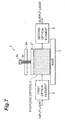
- Fig. 1 is an explanatory diagram of an optical device of an embodiment.
- This optical device is a device that selects a desired wavelength band from the wavelength band of input light and outputs light of this desired wavelength band as output light.
- a photonic crystal 2 is placed on a base 1, and photonic crystal 2 is urged by a pressurizing/depressurizing device (external force application means) 3, which applies pressure or reduces the pressure applied to photonic crystal 2.
- photonic crystal 2 Since photonic crystal 2 has plasticity, when photonic crystal 2 is deformed by the application of external force, the photonic band gap changes greatly and the wavelength of the output light from photonic crystal 2 thus changes adequately. With such an optical device, since effective wavelength selection will be enabled even when the volume of photonic crystal 2 itself is made small, it is possible to make the entire device compact.
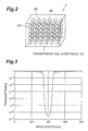
- Fig. 2 is a perspective view of photonic crystal 2.
- microspheres 2B of silica or barium titanate are contained inside a gel substance 2G.
- This photonic crystal 2 can be deformed readily.
- Microspheres 2B are aligned uniformly in a regular manner at a period close to the wavelength of light inside substance 2G.
- the interval between microspheres 2B is half to one-fourth the wavelength of the light that is to be selected, and microspheres 2B are transparent to this wavelength.
- light of a wavelength band ⁇ (which includes ⁇ 1 ) is made to enter photonic crystal 2, only components of a specific wavelength band ⁇ 1 are transmitted through photonic crystal 2 in accordance with the photonic band gap.
- a material having an ultraviolet-curing resin mixed therein may be used as a sol material and gelling may be accomplished by illuminating this material with ultraviolet rays.
- a mixture of a crosslinking agent and a photopolymerization initiator in acrylamide is a representative example of an ultraviolet-curing resin, and various other examples are known since priorly.
- photonic crystal 2 Since it is sufficient for the number of periodic structures of microspheres 2B to be approximately 50, photonic crystal 2 will function adequately even if it is an element with a maximum size of 100 ⁇ m square. Compactness of a device can thus be realized by using this photonic crystal 2.
- the above-described optical device has external force application means 3 for applying the abovementioned external force, and various types of external force application means are possible.
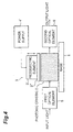
- Fig. 4 is an explanatory diagram, showing a favorable example of the above-described optical device.
- the above-described external force application means 3 is a piezoelectric element (piezo element) 3', which deforms in accordance with an electrical input.
- a voltage variable power supply 4' is used as external pressure control device 4.
- piezoelectric element 3' moves in the direction perpendicular to the surface of base 1 in accordance with the voltage applied from power supply 4'.
- a presser plate 3" is disposed above photonic crystal 2, and together with base 1, presser plate 3" sandwiches photonic crystal 2.
- the upper surface of piezoelectric element 3' is set at a position that is fixed with respect to base 1 and the lower surface is fixed to presser plate 3". Since when piezoelectric element 3' expands or contracts, the distance between presser plate 3" and base 1 changes, photonic crystal 2 deforms in an elongating manner along the optical path.
- piezoelectric element 3' is deformed by an electrical input and applies an external force to photonic crystal 2, a system that performs an electrical input based on a specific measured value, etc., can be arranged.
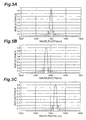
- Figs. 5A, 5B, and 5C are graphs, showing the wavelength (nm) dependence of the transmittance (arbitrary constant) of output light by a photonic crystal with a multilayer film structure, that is, a dichroic mirror.
- Fig. 5A is a graph for the case where an external force is not applied to the dichroic mirror
- Fig. 5B is a graph for the case where a pressure is applied to give rise to a 1% lattice distortion in the direction perpendicular to the mirror
- Fig. 5C is a graph for the case where a pressure is applied to give rise to a 1% lattice distortion in the direction perpendicular to the mirror.
- a pressure may also be applied to give rise to a lattice distortion along the mirror surface.
- the wavelength ⁇ CENTER at which the peak intensity of the reflectance spectrum lies is approximately 1.5 ⁇ m in the case where there is no external force.
- the wavelength ⁇ CENTER shifts to approximately 1470nm (to the shorter wavelength side) when a 1% compressive strain is applied and shifts to 1530nm (to the longer wavelength side) when a 1% expansive strain is applied.
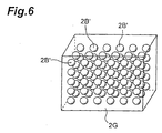
- Fig. 6 is a perspective view of a photonic crystal 2 that uses air bubbles as the abovementioned microscopic spaces.
- This photonic crystal 2 has a plurality of air bubbles 2B' inside a substance 2G, and the air bubbles 2B' take the place of the abovementioned microspheres 2B.
- Such a photonic crystal 2 can also be deformed readily by an external force.
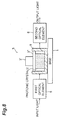
- Fig. 8 is an explanatory diagram of an optical device of another embodiment.
- This optical device is furthermore equipped with a container 9 that houses a photonic crystal 2, and an external force application means 3 applies pressure as an external force in a fixed direction with respect to photonic crystal 2 housed inside container 9.
- photonic crystal 2 may be held by an outer wall of container 9 to restrict deformation due to forces besides the desired external force and limit the direction of deformation.
- a piezoelectric element 3' is used as external force application means 3.
- At least a part of the outer walls of container 9, that is, the optical path for the input light is transparent. Or, a transparent window may be disposed at this part.
- the input light is input into photonic crystal 2 via the transparent wall or window.
- the outer wall in the optical path for the output light may also be transparent. Since photonic crystal 2 is held by the corresponding outer wall, the number of parts required of the device can be reduced.
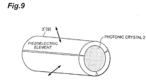
- a tube-type piezoelectric element may also be used as external force application means 3 for photonic crystal 2.
- Piezoelectric element 3' deforms in a manner such that its inner diameter changes, and in accordance with this deformation, photonic crystal 2 deforms in a manner such that it expands or contracts in the length direction of the hollow piezoelectric element.
- the input light is input from one end in the length direction of photonic crystal 2 and the output light is output from the other end.
- Spreading of light in the radial direction can thus be restrained, and by use of this type of piezoelectric element, the lowering of intensity per unit area of the output light can be restrained.
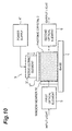
- Fig. 10 is an explanatory diagram of an optical device of yet another embodiment.
- This optical device differs from that shown in Fig. 4 in that a window member 10 is adhered onto the light input surface of a photonic crystal 2, and besides this, the arrangement is the same as that shown in Fig. 4.
- the input light that exits from a first optical element 5 is introduced via window member 10 into photonic crystal 2.
- Window material 10 may also be an optical filter.
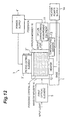
- a physical quantity which varies in accordance with the photonic band gap and is preferably the output light intensity or output light spectrum, is measured and feedback means 11 and 4' are made to control external force application means 3 so that the intensity of output light or the intensity of a specific wavelength will be constant.
- the light that has been modulated by photonic crystal 2 is subject as the output light to measurement of its intensity spectrum by optical characteristic measurement equipment 11 and piezoelectric element 3', which serves as a structure control device, is subject to feedback control so that the measured data will take on a specific value. For example, if the intensity of a specific wavelength that is measured is low, piezoelectric element 3' is made to expand or contract in a predetermined direction and when this causes the intensity to increase, piezoelectric element 3' is made to expand or contract in the same direction, while when the intensity decreases, piezoelectric element 3' is made to expand or contract in the opposite direction.
- Photonic crystal 2 may also be produced using semiconductor microelectromechanic (MEMS) techniques.
- MEMS semiconductor microelectromechanic
- the abovementioned container is formed by processing a semiconductor substrate and piezoelectric element 3' is formed on this semiconductor substrate (not shown).
- semiconductor microelectromechanic techniques can be used to form these components and make the entire device compact.
- a driving circuit for piezoelectric element 3', a power supply, a photodiode with wavelength filter, etc. may also be formed within the semiconductor substrate.
- Semiconductor microelectromechanic techniques are also used to prepare, for example, the probe of a scanning tunnel microscope.
- This probe is provided with a piezoelectric element and expansion and contraction of the piezoelectric element can be controlled in the order of a few nm's.
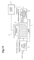
- heater 12 which heats a photonic crystal 2 is disposed on a base 1.
- Temperature sensor 13 which measures the temperature of photonic crystal 2, is also disposed on base 1. These are positioned close to photonic crystal 2.
- Heater power supply 14 controls the power supplied to heater 12 in accordance with the temperature measured by temperature sensor 13.
- the temperature of photonic crystal 2 can be set to a desired value, which is preferably a fixed value, to restrain variation of the photonic band gap due to temperature.
- Heater 12 and temperature sensor 13 may also be formed in a monolithic manner using MEMS techniques.
- a Fabry-Perot interferometer and multilayer film mirror (dichroic mirror) are also 0-dimensional or 1-dimensional photonic crystals.
- Photonic crystal 2 may be applied to such uses. With a soft photonic crystal 2, such as described above, it is anticipated that further research will be carried out on the stability of the sizes and alignment of microspheres 2B or air bubbles 2B', mechanical precision for improving the controllability, long-term stability of the gel, temperature stability, methods of connection with optical fibers and other optical parts, gel-sealing containers, external force application mechanisms that can apply the same external force each time, etc.
- This invention can be used in an optical device that uses a photonic crystal.
Landscapes
- Physics & Mathematics (AREA)
- Optics & Photonics (AREA)
- Engineering & Computer Science (AREA)
- Chemical & Material Sciences (AREA)
- General Physics & Mathematics (AREA)
- Nonlinear Science (AREA)
- Nanotechnology (AREA)
- Life Sciences & Earth Sciences (AREA)
- Biophysics (AREA)
- Crystallography & Structural Chemistry (AREA)
- Microelectronics & Electronic Packaging (AREA)
- Optical Integrated Circuits (AREA)
- Mechanical Light Control Or Optical Switches (AREA)
Abstract
Description
Claims (12)
- An optical device, with which an external force is applied to a photonic crystal to change the photonic band gap of said photonic crystal, wherein said photonic crystal has plasticity.
- The optical device as set forth in Claim 1, furthermore comprising an external force application means for applying said external force.
- The optical device as set forth in Claim 2, furthermore comprising a feedback means, which measures a physical quantity that varies in accordance with the photonic band gap of the photonic crystal and controls the magnitude of said external force applied by said external force application means in accordance with the measured value.
- The optical device as set forth in Claim 1, furthermore comprising a heater, which heats said photonic crystal, and a temperature sensor, which measures the temperature of said photonic crystal, and wherein the power supplied to said heater is controlled in accordance with the temperature measured by said temperature sensor.
- The optical device as set forth in Claim 1, furthermore comprising a container, which houses said photonic crystal, and wherein said external force application means applies pressure in a fixed direction as said external force to said photonic crystal that is housed inside said container.
- The optical device as set forth in Claim 5, wherein at least a part of the outer walls of said container is transparent or a transparent window is disposed at this part and light is input into said photonic crystal via said part.
- The optical device as set forth in Claim 1, wherein said photonic crystal has a plurality of microspheres of silica or barium titanate contained in a gel substance.
- The optical device as set forth in Claim 1, wherein said photonic crystal has a plurality of microscopic spaces formed and contained inside a gel substance.
- The optical device as set forth in Claim 2, wherein said external force application means is a piezoelectric element that deforms in accordance with an electrical input.
- The optical device as set forth in Claim 2, wherein said external force application means is a pressing mechanism that presses said photonic crystal in accordance with a manual input.
- The optical device as set forth in Claim 2, wherein said external force application means is a hollow member, which can be deformed in a manner such that its inner diameter changes, and said photonic crystal is disposed inside said hollow member.
- The optical device as set forth in Claim 5, wherein said container is formed by processing a semiconductor substrate.
Applications Claiming Priority (3)
| Application Number | Priority Date | Filing Date | Title |
|---|---|---|---|
| JP2000292703A JP2002098916A (en) | 2000-09-26 | 2000-09-26 | Optical device |
| JP2000292703 | 2000-09-26 | ||
| PCT/JP2001/008384 WO2002027384A1 (en) | 2000-09-26 | 2001-09-26 | Optical device |
Publications (2)
| Publication Number | Publication Date |
|---|---|
| EP1329758A1 true EP1329758A1 (en) | 2003-07-23 |
| EP1329758A4 EP1329758A4 (en) | 2004-12-08 |
Family
ID=18775606
Family Applications (1)
| Application Number | Title | Priority Date | Filing Date |
|---|---|---|---|
| EP01970226A Withdrawn EP1329758A4 (en) | 2000-09-26 | 2001-09-26 | Optical device |
Country Status (6)
| Country | Link |
|---|---|
| US (1) | US6956689B2 (en) |
| EP (1) | EP1329758A4 (en) |
| JP (1) | JP2002098916A (en) |
| CN (1) | CN1210595C (en) |
| AU (1) | AU2001290279A1 (en) |
| WO (1) | WO2002027384A1 (en) |
Cited By (3)
| Publication number | Priority date | Publication date | Assignee | Title |
|---|---|---|---|---|
| WO2004031821A1 (en) * | 2002-10-01 | 2004-04-15 | Canon Kabushiki Kaisha | Method of controlling optical characteristic of optical element and optical device |
| WO2007098788A1 (en) * | 2005-05-12 | 2007-09-07 | Merck Patent Gmbh | Force sensor |
| US7272272B2 (en) | 2002-10-01 | 2007-09-18 | Canon Kabushiki Kaisha | Optical deflector based on photonic bandgap structure |
Families Citing this family (20)
| Publication number | Priority date | Publication date | Assignee | Title |
|---|---|---|---|---|
| JP4627362B2 (en) * | 2000-09-26 | 2011-02-09 | 浜松ホトニクス株式会社 | Tunable light source |
| JP4619507B2 (en) * | 2000-09-26 | 2011-01-26 | 浜松ホトニクス株式会社 | Optical fiber coupling device, wavelength tunable device, pressure sensor, acceleration sensor, and optical device |
| JP3743637B2 (en) * | 2001-08-23 | 2006-02-08 | 独立行政法人理化学研究所 | Photonic crystal and optical waveguide element |
| US7068904B2 (en) * | 2002-10-01 | 2006-06-27 | Canon Kabushiki Kaisha | Optical element with periodic structure |
| JP4978943B2 (en) * | 2003-12-17 | 2012-07-18 | オリンパス株式会社 | Photonic crystal |
| JP2008518455A (en) * | 2004-10-27 | 2008-05-29 | コーニンクレッカ フィリップス エレクトロニクス エヌ ヴィ | Semiconductor device having adjustable energy band gap |
| US7550755B2 (en) * | 2004-10-27 | 2009-06-23 | Philips Lumiled Lighting Co., Llc | Semiconductor device with tunable energy band gap |
| WO2008098339A1 (en) * | 2007-02-16 | 2008-08-21 | The Governing Council Of The University Of Toronto | Compressible photonic crystal |
| WO2009143625A1 (en) | 2008-05-30 | 2009-12-03 | Opalux Incorporated | Tunable bragg stack |
| US8736952B2 (en) | 2008-08-20 | 2014-05-27 | Opalux Incorporated | Photonic crystal device |
| US9599515B2 (en) * | 2009-02-25 | 2017-03-21 | Opalux Incorporated | Temperature-responsive photonic crystal device |
| JP5056786B2 (en) * | 2009-03-30 | 2012-10-24 | 豊田合成株式会社 | Display device |
| US8363303B2 (en) * | 2010-03-30 | 2013-01-29 | Honeywell International Inc. | Photonic structures and photonic devices |
| CN102087382A (en) * | 2010-12-13 | 2011-06-08 | 华北电力大学(保定) | Fabrication method of isotropic photonic crystal with full-space forbidden band structure |
| AU2011342264B2 (en) * | 2010-12-14 | 2015-11-19 | Opalux Incorporated | Photonic crystal device with offset activation |
| CN102263359B (en) * | 2011-06-17 | 2012-09-26 | 华北电力大学(保定) | Q-switched photonic crystal fiber laser |
| US20120325001A1 (en) * | 2011-06-27 | 2012-12-27 | The Boeing Company | Optical sensor systems and methods |
| KR101902924B1 (en) * | 2012-11-14 | 2018-10-01 | 삼성전자주식회사 | Light emitting apparatus capable of tuning color of light emitted therefrom |
| TWI619234B (en) | 2015-10-30 | 2018-03-21 | 瑞昱半導體股份有限公司 | Integrated circuit |
| CN112965268B (en) * | 2021-02-05 | 2022-07-05 | 中山蓝宏科技有限公司 | Flexible photonic crystal with multi-angle photochromic effect and preparation method thereof |
Family Cites Families (10)
| Publication number | Priority date | Publication date | Assignee | Title |
|---|---|---|---|---|
| ATE71718T1 (en) * | 1987-06-04 | 1992-02-15 | Walter Lukosz | OPTICAL MODULATION AND MEASUREMENT PROCEDURE. |
| US5385114A (en) * | 1992-12-04 | 1995-01-31 | Milstein; Joseph B. | Photonic band gap materials and method of preparation thereof |
| US5982518A (en) * | 1996-03-27 | 1999-11-09 | Ciena Corporation | Optical add-drop multiplexers compatible with very dense WDM optical communication systems |
| GB9713018D0 (en) | 1997-06-20 | 1997-08-27 | Secr Defence | Optical fibre bend sensor |
| GB9903918D0 (en) * | 1999-02-19 | 1999-04-14 | Univ Bath | Improvements in and relating to photonic crystal fibres |
| JP3516159B2 (en) * | 2000-03-03 | 2004-04-05 | 日本航空電子工業株式会社 | Method for manufacturing photonic crystal element |
| CA2417747C (en) * | 2000-07-31 | 2009-11-24 | Naomi Matsuura | Configurable photonic device |
| WO2002014913A1 (en) * | 2000-08-15 | 2002-02-21 | Corning Incorporated | Active photonic crystal waveguide device |
| JP4627362B2 (en) * | 2000-09-26 | 2011-02-09 | 浜松ホトニクス株式会社 | Tunable light source |
| JP4619507B2 (en) * | 2000-09-26 | 2011-01-26 | 浜松ホトニクス株式会社 | Optical fiber coupling device, wavelength tunable device, pressure sensor, acceleration sensor, and optical device |
-
2000
- 2000-09-26 JP JP2000292703A patent/JP2002098916A/en active Pending
-
2001
- 2001-09-26 AU AU2001290279A patent/AU2001290279A1/en not_active Abandoned
- 2001-09-26 WO PCT/JP2001/008384 patent/WO2002027384A1/en not_active Ceased
- 2001-09-26 US US10/381,318 patent/US6956689B2/en not_active Expired - Lifetime
- 2001-09-26 EP EP01970226A patent/EP1329758A4/en not_active Withdrawn
- 2001-09-26 CN CNB018163289A patent/CN1210595C/en not_active Expired - Fee Related
Cited By (4)
| Publication number | Priority date | Publication date | Assignee | Title |
|---|---|---|---|---|
| WO2004031821A1 (en) * | 2002-10-01 | 2004-04-15 | Canon Kabushiki Kaisha | Method of controlling optical characteristic of optical element and optical device |
| US7136560B2 (en) | 2002-10-01 | 2006-11-14 | Canon Kabushiki Kaisha | Method of controlling optical characteristic of optical element and optical device |
| US7272272B2 (en) | 2002-10-01 | 2007-09-18 | Canon Kabushiki Kaisha | Optical deflector based on photonic bandgap structure |
| WO2007098788A1 (en) * | 2005-05-12 | 2007-09-07 | Merck Patent Gmbh | Force sensor |
Also Published As
| Publication number | Publication date |
|---|---|
| CN1466700A (en) | 2004-01-07 |
| CN1210595C (en) | 2005-07-13 |
| US6956689B2 (en) | 2005-10-18 |
| EP1329758A4 (en) | 2004-12-08 |
| US20040012840A1 (en) | 2004-01-22 |
| JP2002098916A (en) | 2002-04-05 |
| AU2001290279A1 (en) | 2002-04-08 |
| WO2002027384A1 (en) | 2002-04-04 |
Similar Documents
| Publication | Publication Date | Title |
|---|---|---|
| US6956689B2 (en) | Optical device | |
| EP1324099B1 (en) | Optical fiber connector and optical device | |
| EP0593836B1 (en) | Near-field photon tunnelling devices | |
| US5774259A (en) | Photorestrictive device controller and control method therefor | |
| JP4627362B2 (en) | Tunable light source | |
| Zhang et al. | A low loss quantum-dot-doped optical fiber temperature sensor based on flexible print technology | |
| EP1279998B1 (en) | Tunable Fabry-Perot cavity filter and method for making and using the filter | |
| JP2002350908A (en) | Light beam deflecting device using photonic crystal, optical switch using the same, and light beam deflecting method | |
| JP4514984B2 (en) | Optical waveform shaping device | |
| JP5120909B2 (en) | Method for producing colloidal crystal gel, colloidal crystal gel, and optical element | |
| Joshi | Advances in development of MOEMS devices: a review | |
| US7142572B2 (en) | Wavelength conversion laser apparatus with tunable fiber Bragg grating | |
| JP2013142867A (en) | Ultrasonic variable-focal length lens array and control method of the same | |
| KR100399588B1 (en) | Electrically Controllable Liquid Crystal Optical Fiber Grating Device | |
| Lawrence | LY Lin, SS Lee, KSJ Pister and MC Wu | |
| WO2004031820A1 (en) | Optical deflector based on photonic bandgap structure | |
| Chang et al. | Surface micromachined devices for microwave and photonic applications | |
| JP2004145315A (en) | Optical element and modulation method of optical element | |
| Roxworthy et al. | Electro-Optic Switching and Regenerative Oscillation of a Localized Gap Plasmomechanical Resonator | |
| Song et al. | Novel tuning method for optofluidics | |
| JP2004145314A (en) | Optical element having periodic structure, mirror having the optical element, optical deflector, and method of controlling optical element | |
| Khoo et al. | Direct optical holographic fabrication of photonic crystals in polymeric dispersed nematic and isotropic liquid crystals | |
| JP2004145317A (en) | Optical deflecting device, optical switch constituted by the optical deflecting device, optical scanning device, and optical deflecting method | |
| JPH0132488B2 (en) |
Legal Events
| Date | Code | Title | Description |
|---|---|---|---|
| PUAI | Public reference made under article 153(3) epc to a published international application that has entered the european phase |
Free format text: ORIGINAL CODE: 0009012 |
|
| 17P | Request for examination filed |
Effective date: 20030417 |
|
| AK | Designated contracting states |
Designated state(s): AT BE CH CY DE DK ES FI FR GB GR IE IT LI LU MC NL PT SE TR |
|
| AX | Request for extension of the european patent |
Extension state: AL LT LV MK RO SI |
|
| RBV | Designated contracting states (corrected) |
Designated state(s): DE FR GB |
|
| RIC1 | Information provided on ipc code assigned before grant |
Ipc: 7G 02B 6/12 B Ipc: 7G 02B 26/00 A |
|
| A4 | Supplementary search report drawn up and despatched |
Effective date: 20041021 |
|
| 17Q | First examination report despatched |
Effective date: 20050113 |
|
| 17Q | First examination report despatched |
Effective date: 20050113 |
|
| STAA | Information on the status of an ep patent application or granted ep patent |
Free format text: STATUS: THE APPLICATION IS DEEMED TO BE WITHDRAWN |
|
| 18D | Application deemed to be withdrawn |
Effective date: 20070323 |