EP1329700A1 - Optical measurement apparatus and method for optical measurement - Google Patents
Optical measurement apparatus and method for optical measurement Download PDFInfo
- Publication number
- EP1329700A1 EP1329700A1 EP00962814A EP00962814A EP1329700A1 EP 1329700 A1 EP1329700 A1 EP 1329700A1 EP 00962814 A EP00962814 A EP 00962814A EP 00962814 A EP00962814 A EP 00962814A EP 1329700 A1 EP1329700 A1 EP 1329700A1
- Authority
- EP
- European Patent Office
- Prior art keywords
- signal
- time
- optical measurement
- outputting
- photons
- Prior art date
- Legal status (The legal status is an assumption and is not a legal conclusion. Google has not performed a legal analysis and makes no representation as to the accuracy of the status listed.)
- Withdrawn
Links
Images



Classifications
-
- G—PHYSICS
- G01—MEASURING; TESTING
- G01J—MEASUREMENT OF INTENSITY, VELOCITY, SPECTRAL CONTENT, POLARISATION, PHASE OR PULSE CHARACTERISTICS OF INFRARED, VISIBLE OR ULTRAVIOLET LIGHT; COLORIMETRY; RADIATION PYROMETRY
- G01J1/00—Photometry, e.g. photographic exposure meter
- G01J1/42—Photometry, e.g. photographic exposure meter using electric radiation detectors
- G01J1/44—Electric circuits
-
- H—ELECTRICITY
- H04—ELECTRIC COMMUNICATION TECHNIQUE
- H04N—PICTORIAL COMMUNICATION, e.g. TELEVISION
- H04N25/00—Circuitry of solid-state image sensors [SSIS]; Control thereof
- H04N25/70—SSIS architectures; Circuits associated therewith
- H04N25/76—Addressed sensors, e.g. MOS or CMOS sensors
- H04N25/77—Pixel circuitry, e.g. memories, A/D converters, pixel amplifiers, shared circuits or shared components
- H04N25/772—Pixel circuitry, e.g. memories, A/D converters, pixel amplifiers, shared circuits or shared components comprising A/D, V/T, V/F, I/T or I/F converters
- H04N25/773—Pixel circuitry, e.g. memories, A/D converters, pixel amplifiers, shared circuits or shared components comprising A/D, V/T, V/F, I/T or I/F converters comprising photon counting circuits, e.g. single photon detection [SPD] or single photon avalanche diodes [SPAD]
-
- G—PHYSICS
- G01—MEASURING; TESTING
- G01J—MEASUREMENT OF INTENSITY, VELOCITY, SPECTRAL CONTENT, POLARISATION, PHASE OR PULSE CHARACTERISTICS OF INFRARED, VISIBLE OR ULTRAVIOLET LIGHT; COLORIMETRY; RADIATION PYROMETRY
- G01J1/00—Photometry, e.g. photographic exposure meter
- G01J1/42—Photometry, e.g. photographic exposure meter using electric radiation detectors
- G01J1/44—Electric circuits
- G01J2001/4413—Type
- G01J2001/442—Single-photon detection or photon counting
-
- G—PHYSICS
- G01—MEASURING; TESTING
- G01J—MEASUREMENT OF INTENSITY, VELOCITY, SPECTRAL CONTENT, POLARISATION, PHASE OR PULSE CHARACTERISTICS OF INFRARED, VISIBLE OR ULTRAVIOLET LIGHT; COLORIMETRY; RADIATION PYROMETRY
- G01J1/00—Photometry, e.g. photographic exposure meter
- G01J1/42—Photometry, e.g. photographic exposure meter using electric radiation detectors
- G01J1/44—Electric circuits
- G01J2001/4413—Type
- G01J2001/4433—Peak sensing
-
- G—PHYSICS
- G01—MEASURING; TESTING
- G01J—MEASUREMENT OF INTENSITY, VELOCITY, SPECTRAL CONTENT, POLARISATION, PHASE OR PULSE CHARACTERISTICS OF INFRARED, VISIBLE OR ULTRAVIOLET LIGHT; COLORIMETRY; RADIATION PYROMETRY
- G01J1/00—Photometry, e.g. photographic exposure meter
- G01J1/42—Photometry, e.g. photographic exposure meter using electric radiation detectors
- G01J1/44—Electric circuits
- G01J2001/444—Compensating; Calibrating, e.g. dark current, temperature drift, noise reduction or baseline correction; Adjusting
-
- G—PHYSICS
- G01—MEASURING; TESTING
- G01J—MEASUREMENT OF INTENSITY, VELOCITY, SPECTRAL CONTENT, POLARISATION, PHASE OR PULSE CHARACTERISTICS OF INFRARED, VISIBLE OR ULTRAVIOLET LIGHT; COLORIMETRY; RADIATION PYROMETRY
- G01J1/00—Photometry, e.g. photographic exposure meter
- G01J1/42—Photometry, e.g. photographic exposure meter using electric radiation detectors
- G01J1/44—Electric circuits
- G01J2001/4446—Type of detector
- G01J2001/446—Photodiode
- G01J2001/4466—Avalanche
Definitions
- the present invention relates to an optical measurement apparatus and a method for optical measurement, and particularly to an optical measurement apparatus and method for optical measurement for detecting photons.
- the conventional tool such as a photomultiplier tube, for measuring light is not a tool for measuring light in time and space at the photon level.
- a digital oscilloscope for example, to observe output from an avalanche photodiode, which is capable of detecting light at the photon level, is a conceivable method for measuring light in time and space at the photon level.
- the digital oscilloscope because the oscilloscope is not designed for detecting photons, the digital oscilloscope has a higher resolution than necessary. Accordingly, as a tradeoff for the high resolution, the oscilloscope is drastically limited in the length of time that the oscilloscope can perform measurements.
- the present invention is to solve the above-described problems. It is an objective of the present invention to provide an optical measurement apparatus and a method for optical measurement capable of measuring "when photons arrive” or "how many photons have arrived” over a long period of time.
- the present invention provides an optical measurement apparatus, comprising: a photon detecting portion detecting incident photons; a time signal outputting portion outputting time signals; and a storing portion storing a time signal that is outputted from the time signal outputting portion at the time when the photon detecting portion detects photons.
- the optical measurement apparatus can measure when photons have arrived by storing a time signal that is outputted from the time signal outputting portion when the photon detecting portion detects photons. On the other hand, no data is stored in the storing portion when the photon detecting portion does not detect photons. Accordingly, the amount of data stored in the storing portion is extremely small. As a result, the optical measurement apparatus can measure, over a long period of time, when photons have arrived.
- the photon detecting portion detects the number of the incident photons, and wherein the storing portion stores, when the photon detecting portion detects photons, both the number of photons detected by the photon detecting portion and the time signal outputted by the time signal outputting portion.
- the optical measurement apparatus can measure when and how many photons have arrived by storing, when the photon detecting portion detects photons, the number of the photons detected by the photon detecting portion and a time signal that is outputted from the time signal outputting portion when the photon detecting portion detects photons.
- no data is stored in the storing portion when the photon detecting portion does not detect photons. Accordingly, the amount of data stored in the storing portion is extremely small. As a result, the optical measurement apparatus can measure over a long period of time when and how many photons have arrived.
- the photon detecting portion includes an analog-to-digital converter outputting the number of the incident photons in a digital value.
- the signal outputted from the photon detecting portion can be directly stored in the storing portion.
- the photon detecting portion includes: a photocathode emitting photoelectrons that correspond to the number of the incident photons; an accelerating portion accelerating the photoelectrons emitted from the photocathode; and a semiconductor photodetector receiving the photoelectrons accelerated by the accelerating portion and outputting an output signal that corresponds to the number of the photoelectrons.
- the photon detecting portion that is provided with the photocathode, the accelerating portion, and the semiconductor photodetector, it is possible to efficiently detect the number of photons that fall incident simultaneously (or at nearly the same timings).
- the semiconductor photodetector includes an avalanche photodiode.
- the present invention provides an optical measurement method, comprising: a photon detecting step detecting incident photons; a time signal outputting step outputting time signals; and a storing step storing a time signal that is outputted from the time signal outputting step at the time when the photon detecting step detects photons.
- the optical measurement method can measure when photons have arrived by storing a time signal that is outputted at the time signal outputting step when the photon detecting step detects photons.
- no data is stored by the storing step when the photon detecting step does not detect photons. Accordingly, the amount of data stored by the storing step is extremely small.
- the photon detecting step detects a plurality of incident photons in separation from one another, wherein the storing step stores, when the photon detecting step detects photons, both the number of photons detected by the photon detecting step and the time signal outputted by the time signal outputting step.
- the optical measurement method can measure when and how many photons have arrived by storing, when the photon detecting step detects photons, the number of the photons detected by the photon detecting step and a time signal that is outputted at the time signal outputting step when the photon detecting step detects photons.
- no data is stored by the storing step when the photon detecting step does not detect photons. Accordingly, the amount of data stored by the storing step is extremely small. As a result, the optical measurement method can measure over a long period of time when and how many photons have arrived.
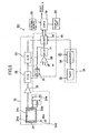
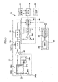
- Fig. 1 shows the construction of this optical measurement apparatus.
- An optical measurement apparatus 10 includes a photon detection unit 12 for detecting incident photons, a time signal output unit 14 for outputting a time signal, a storage unit 16 for storing time signals outputted from the time signal output unit 14 when the photon detection unit 12 detects photons, a CPU 18 for controlling overall operations of the device, an external memory 20 for storing settings and the like, and a display unit 22 for displaying measurement results and the like.
- a photon detection unit 12 for detecting incident photons
- a time signal output unit 14 for outputting a time signal
- a storage unit 16 for storing time signals outputted from the time signal output unit 14 when the photon detection unit 12 detects photons
- a CPU 18 for controlling overall operations of the device
- an external memory 20 for storing settings and the like
- a display unit 22 for displaying measurement results and the like.
- the photon detection unit 12 includes a hybrid photodetector (hereinafter referred to as the HPD 24), a transimpedance amplifier (hereinafter referred to as the TZ amplifier 26), a peak holding circuit 28, and an A/D (analog-to-digital) converter 30.
- HPD 24 hybrid photodetector
- TZ amplifier 26 transimpedance amplifier
- A/D (analog-to-digital) converter 30 an A/D (analog-to-digital) converter 30.
- the HPD 24 is an electron tube having a photocathode 24a for emitting photoelectrons corresponding to the number of incident photons and an avalanche photodiode (hereinafter referred to as an APD 24b), which is a semiconductor photodetector for outputting an output signal corresponding to the number of photoelectrons emitted from the photocathode 24a.
- the photocathode 24a and APD 24b are disposed opposing each other in a vacuum chamber 24c.
- a high-voltage source 24d applies a high negative voltage (for example, -8 kV) to the photocathode 24a, while a bias circuit 24e applies a reverse bias voltage (for example, - 150 V) across an anode and a cathode of the APD 24b.
- An electronic lens unit not shown in the diagram is also provided in the HPD 24, enabling the photoelectrons emitted from the photocathode 24a to be efficiently impinged on the APD 24b.
- the multiplication factor of the first stage is dependent on the acceleration voltage of the electrons (the voltage applied to the photocathode), and is approximately 1,200 when the voltage is -8 kV.
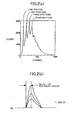
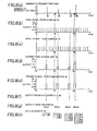
- the electrons are further amplified through avalanche multiplication to about 50 times, resulting in a gain of approximately 60,000 times through the effects of the entire APD 24b. Since the multiplication factor of approximately 1,200 in the first stage is extremely large, the multiplication fluctuations in the HPD 24 that uses the APD 24b are extremely small. Accordingly, the distribution of outputted wave heights shown in Fig. 2(a) are obtained from the HPD 24 when the HPD 24 receives multiple photons. With this HPD 24, it is possible to detect how many photons fall incident thereon. The results shown in Fig. 2(a) were obtained when applying a voltage of -8 kV to the photocathode 24a and a reverse bias voltage of -150 V to the APD 24b and conducting measurements using an Oltec model no. 142A preamplifier.
- the gain of the HPD 24 is about 60,000 and the full-width half-maximum (FWHM) of the output waveform from the HPD 24 corresponding to one electron is about 2 ns, the peak current outputted from the HPD 24 is about 5 ⁇ A per photon. (The photon-electron conversion efficiency is set to 100% for convenience.)
- the electron tubes disclosed in Japanese unexamined patent application publications Nos. HEI-9-312145 and HEI-6-318447, a photomultiplier tube disclosed in Japanese unexamined patent application publication No. HEI-8-148113, and an electron tube disclosed in Japanese unexamined patent application publication No. HEI-9-297055 can be widely used.
- the TZ amplifier 26 is a current-to-voltage converting circuit that amplifies the current signal outputted from the APD 24b, that converts the signal to a voltage, and that outputs the voltage.
- the output waveform of the TZ amplifier 26 is shown in Fig. 2(b).
- the time required for the voltage to rise from 0 V to the maximum voltage is fixed and not dependent on the magnitude of the input signal.
- the TZ amplifier 26 preferably has a gain for amplifying 1 ⁇ A to about 50 mV and should have a bandwidth of about 300 MHz.
- a good example of the TZ amplifier 26 is the AU-1494-300 (model) manufactured by Miteq, or the like.
- the peak voltage outputted from the TZ amplifier 26 according to the above gain is about 0.25 V per photon.
- the peak holding circuit 28 holds the peak value of the output signal from the TZ amplifier 26 for a fixed period of time and outputs this peak value.
- the peak value outputted from the peak holding circuit 28 is reset when a reset signal is received from the time signal output unit 14.
- the A/D converter 30 Upon receiving a trigger signal from the storage unit 16, the A/D converter 30 performs A/D (analog-to-digital) conversion on the signal outputted from the peak holding circuit 28 and outputs the converted signal.
- the resolution of the A/D converter 30 is adjusted to output the number of incident photons as a digital value.
- the input range (0-1 V) is divided into 4 gradations, such that a digital value of "1” is outputted when the input voltage is 0.125-0.375 V, a digital value of "2” is outputted when the input voltage is 0.375-0.625 V, a digital value of "3” is outputted when the input voltage is 0.625-0.875 V, and a digital value of "4" is outputted when the input voltage is greater than or equal to 0.875 V.
- a digital value of "1" is outputted from the A/D converter 30 when a single photon impinges on the HPD 24, a digital value of "2” is outputted when two photons impinge on the HPD 24, a digital value of "3” is outputted when three photons impinge on the HPD 24, and a digital value of "4" is outputted when four photons impinge on the HPD 24.
- the time signal output unit 14 includes a timer 32 and a counter 34.
- the timer 32 generates and outputs a pulse signal at a fixed time interval (for example, 5 ns).
- the counter 34 receives the pulse signal from the timer 32 and outputs a reset signal (the reset signal A in Fig. 1) to the peak holding circuit 28 at the fixed time interval (for example, 5 ns).
- the counter 34 counts pulse signals received from the timer 32 and outputs the result of multiplying the period of pulse signals (for example, 5 ns) by the count number to the storage unit 16 as a time signal.
- the time interval of the pulse signals generated by the timer 32 should be as short as possible for improving precision because the time interval of the pulse signal determines the time resolution of the optical measurement apparatus 10, but should be longer than the time width of a response wave that the HPD 24 outputs in response to incidence of a single photon. This is because a single event will erroneously be counted multiple times if the time interval of the pulse signal were shorter than the response waveform for a single photon.
- the counter 34 is reset by a reset signal from the CPU 18 (the reset signal B) in Fig. 1 at the beginning of a measurement and the like.
- the storage unit 16 includes a comparator 36, a delay circuit 37 for A/D conversion, and a memory 38.
- the output signal from the peak holding circuit 28 is inputted into the plus input terminal of the comparator 36, while a reference voltage is inputted into the minus input terminal.
- the reference voltage is set to 0.13 V, which is less than a voltage that is outputted from the peak holding circuit 28 (0.25 V) in response to incidence of one photon.
- the comparator 36 compares the output signal from the peak holding circuit 28 to the reference voltage and outputs a comparison result signal.
- the output signal from the peak holding circuit 28 is larger than the reference voltage, then the output rises at the high level; and when the output signal from the peak holding circuit 28 is smaller than the reference voltage, the output drops to the low level.
- the output from the comparator 36 is transmitted as a trigger signal to both of the A/D converter 30 and the memory 38.
- the value of the delay 1 applied by the delay circuit 37 is set to a value equivalent to or slightly greater than the time required for the output waveform of the TZ amplifier 26 to travel from 0 V to the peak voltage (Fig. 2(b)).
- the memory 38 stores a time signal outputted from the counter 34 and the output signal outputted from the A/D converter 30 at the timing when a trigger signal is received from the delay circuit 37.
- the operations of the storage unit 16 having the construction described above are as follows. Since a trigger signal is not outputted from the delay circuit 37 while photons do not impinge on the HPD 24, data is not stored in the memory 38. However, when photons impinge on the HPD 24, the delay circuit 37 outputs a trigger signal to the A/D converter 30 and the memory 38. In this case, a digital value for the number of photons is outputted from the A/D converter 30 and stored in the memory 38, and a time signal outputted from the counter is also stored in the memory 38.
- the CPU 18 outputs a reset signal to the counter 34 to reset the counter 34.
- the counter 34 begins counting pulse signals received from the timer 32.
- the delay circuit 37 Since output from the HPD 24 and TZ amplifier 26 are small until photons are detected by the HPD 24, that is, from the measurement start time until 59 ns have elapsed, and the output from the peak holding circuit 28 does not exceed the reference voltage, the delay circuit 37 does not output a trigger signal and data is not stored in the memory 38.
- the peak holding circuit 28 detects an output signal from the TZ amplifier 26, and this detection result is outputted to the A/D converter 30 and comparator 36 (Fig. 3(c)).
- this peak value is saved for a prescribed interval by the peak holding circuit 28 and continuously outputted to the A/D converter 30 and comparator 36 (Fig. 3(c)).
- the output from the comparator 36 is set to high level.
- this high level output is outputted as a trigger signal to the A/D converter 30 and memory 38 (Fig. 3(d)).
- a trigger signal is inputted into the A/D converter 30 from the delay circuit 37 in this way, the A/D converter 30 performs A/D conversion on the signal inputted from the peak holding circuit 28.
- the delay 1 is set equivalent to or slightly longer than the time required for the output waveform from the TZ amplifier 26 to travel from 0 V to the peak voltage.
- the peak value of the output signal from the TZ amplifier 26 of about 0.75 V is inputted into the A/D converter 30 at the instant when a trigger signal is inputted into the A/D converter 30. Therefore, the digital value "3" is outputted from the A/D converter 30, as shown in Fig. 3(f).
- the output value from the A/D converter 30 and the time signal outputted from the counter 34 are stored in the memory 38.
- the value of a time signal, which is inputted from the counter 34 first after a trigger signal has been inputted into the memory 38 is stored in the memory 38.
- reset signals are outputted from the counter 34 to the peak holding circuit 28 repeatedly at the fixed time interval (for example 5 ns), as shown in Fig. 3(e). Accordingly, the output signal of the peak holding circuit 28 is reset repeatedly at the fixed time interval (for example, 5 ns), as shown in Fig. 3(c).
- the number of incident photons and the time signal at the photon-incident time are stored in the memory 38.
- the data stored in the memory 38 is similar to that shown in Fig. 3(h).
- the optical measurement apparatus 10 primarily includes the photon detection unit 12 for detecting incident photons, the time signal output unit 14 for outputting time signals, and the storage unit 16 for storing time signals that are outputted from the time signal output unit 14 when the photon detection unit 12 detects photons.
- the photon detection unit 12 includes the HPD 24 having the photocathode 24a and APD 24b, the TZ amplifier 26, the peak holding circuit 28, and the A/D converter 30.
- the time signal output unit 14 includes the timer 32 and counter 34.
- the storage unit 16 includes the comparator 36, delay circuit 37 for A/D conversion, and memory 38. When photons impinge on the HPD 24, the delay circuit 37 outputs a trigger signal, triggering the photon-number, outputted from the A/D converter 30, along with the time data outputted from the counter 34 to be stored in the memory 38.
- the optical measurement apparatus 10 of the present embodiment can measure when and how many photons have arrived.
- the capacity of the memory 38 can be used effectively, and the optical measurement apparatus 10 can measure, over a long period of time, when and how many photons have arrived.
- the optical measurement apparatus 10 of the present embodiment with a 64-MB memory, it is possible to measure and record up to a maximum of 16 million events (incidence of photons), during the measuring time of 150 seconds, with the time resolution of 5 ns.
- the external memory 20 By further employing the external memory 20, it is possible to measure and record for an even longer time.
- the A/D converter 30 outputs the number of incident photons as a digital value. Accordingly, signals outputted from the A/D converter 30 can be directly stored in the memory 38 and directly displayed on the display unit 22.
- the optical measurement apparatus 10 employs the HPD 24 provided with the photocathode 24a and APD 24b, making it possible to efficiently detect the number of photons that impinge on the HPD 24 simultaneously (or at extremely close timings).
- the HPD 24 is used as the photodetector.
- a VLPC visual light photon counter
- the VLPC is formed of an arsenic-doped silicon substrate and a thin, non-doped epitaxial layer on the silicon substrate.
- Avalanche multiplication is generated by cooling the VLPC to about 7 K and applying about 7 V thereto, obtaining a gain of about 5 X 10 4 .
- Such a high gain can be obtained using VLPC because the band gap can be considered as equivalent to the ionization energy produced from the impurity level.
- the VLPC like the HPD, can differentiate and output the number of incident photons.
- optical measurement apparatus 10 The following variations are conceivable for the optical measurement apparatus 10 according to the present embodiment.
- the optical measurement apparatus 50 is provided with a delay circuit 29 for outputting a reset signal to the peak holding circuit 28.
- a trigger signal outputted from the delay circuit 37 is inputted into the delay circuit 29.
- the input voltage of the comparator 36 becomes larger than the reference voltage, causing a trigger signal to be outputted from the delay circuit 37.
- the A/D converter 30 converts the output signal from the peak holding circuit 28 from analog to digital and outputs the converted result to the memory 38.
- the memory 38 having received the same trigger signal, stores the output signal from the A/D converter 30 and the time signal from the counter 34. Further, after being applied with a prescribed delay 2 by the delay circuit 29, the trigger signal is outputted to the peak holding circuit 28 as a reset signal. Accordingly, the peak holding circuit 28 is reset after a fixed time has elapsed since the trigger signal has been outputted from the delay circuit 37.
- Fig. 6(a)-6(h) are timing charts showing the operations of the optical measurement apparatus 50.
- the point, at which the operations of the optical measurement apparatus 50 differ from those of the optical measurement apparatus 10 according to the embodiment described above, is that the peak holding circuit 28 is reset in response to a trigger signal generated by the delay circuit 37, that is, in response to incidence of photons.
- This reset signal is generated by delaying the trigger signal from the delay circuit 37 a fixed delay 2 with the delay circuit 29. Accordingly, the peak holding circuit 28 is reset after the A/D converter 30 performs A/D conversion.
- the optical measurement apparatus 50 can record the number of photons at each photon-incident event and the time of each photon-incident event.
- Fig. 7 shows the construction of an optical measurement apparatus 60 according to a second variation of the preferred embodiment.
- the current signal outputted from the HPD 24 is converted to a voltage by the TZ amplifier 26, and the peak holding circuit 28 outputs an output signal that is resulted by holding the peak value for the fixed time period.
- these functions can be achieved by a charge amplifier 40 with reset function, as in the optical measurement apparatus 60 of the present variation.
- the charge amplifier 40 includes an operational amplifier 40a, a capacitor 40b, and a reset switch 40c. A first input terminal of the operational amplifier 40a is grounded, and the output current from the HPD 24 is inputted into a second input terminal.
- the output terminal of the operational amplifier 40a is connected to the input terminal of the A/D converter 30 and the plus input terminal of the comparator 36.
- the capacitor 40b is connected to the second input terminal of the operational amplifier 40a and the output terminal of the operational amplifier 40a.
- the reset switch 40c is connected in parallel with the capacitor 40b.
- the charge amplifier 40 integrates the electrical charge outputted from the HPD 24 and outputs the voltage resulting from the integration, and is reset when the reset switch 40c is turned ON by a reset signal outputted from the counter 34 (reset signal A in Fig. 7).
- the comparator 36 compares the output voltage from the charge amplifier 40 to a reference voltage and switches its logical output to the high level when the output voltage is greater than the reference voltage and to the low level when the output level is smaller than the reference voltage.
- the high level logic output is outputted as a trigger signal.
- Figs. 8(a)-8(h) are timing charts.
- the counter 34 in the time signal output unit 14 of the optical measurement apparatus 60 outputs a read signal (read signal C in Fig. 7) just prior to outputting a reset signal (Figs. 8(b) and 8(c)).
- An AND circuit 42 is provided downstream from the comparator 36 in the storage unit 16.
- the read signal outputted from the counter 34 and the trigger signal outputted from the comparator 36 (Fig. 8(e)) are inputted into the AND circuit 42.
- the AND circuit 42 outputs an output signal to the A/D converter 30 and the memory 38. Accordingly, the A/D converter 30 performs A/D conversion at the instant when the read signal is outputted from the counter 34 after the output voltage from the charge amplifier 40 (Fig. 8(d)) exceeds the reference voltage.
- the output signal from the A/D converter 30 is stored along with the time signal from the counter 34 in the memory 38. This construction eliminates the need for providing the peak holding circuit 28 and the delay circuit 37 of the embodiment described above. Further, the optical measurement apparatus 60 can minimize errors when a plurality of photons are continuously impinged within a short time.
- the counter 34 is reset by a reset signal outputted from the CPU 18 at the beginning of a measurement.
- the counter 34 can be reset by the trigger signal from the delay circuit 37, as in an optical measurement apparatus 70 according to a third variation shown in Fig. 9.
- the time signal outputted from the counter 34 indicates the time interval at which photons fall incident on the HPD 24 successively. Accordingly, the number of photons falling incident on the HPD 24 and the time interval at which the photons fall incident on the HPD 24 are stored in the memory 38.
- optical measurement apparatus 10 employs the APD 24b as the semiconductor photodetector, a photodiode or the like can also be used.
- optical measurement apparatus and method for optical measurement of the present invention are not limited to the embodiments described above. Many modifications and variations may be made therein.
- a time signal which is inputted from the counter 34 at the first time after the trigger signal has been inputted into the memory 38, is stored in the memory 38 in the optical measurement apparatus and method for optical measurement of the preferred embodiment.
- optical measurement apparatus and method for optical measurement according to the present invention are widely used in the detection of bioluminescence.
Landscapes
- Physics & Mathematics (AREA)
- General Physics & Mathematics (AREA)
- Spectroscopy & Molecular Physics (AREA)
- Engineering & Computer Science (AREA)
- Multimedia (AREA)
- Signal Processing (AREA)
- Photometry And Measurement Of Optical Pulse Characteristics (AREA)
Abstract
An optical measurement apparatus 10 primarily
includes: a photon detection unit 12 for detecting incident
photons, a time signal output unit 14 for outputting a time
signal, and a storage unit 16 for storing the time signal
outputted from the time signal output unit 14 when the
photon detection unit 12 detects photons. The photon
detection unit 12 includes a HPD 24 having a photocathode
24a and an APD 24b, a TZ amplifier 26, a peak holding
circuit 28, and an A/D converter 30. The time signal output
unit 14 includes a timer 32 and a counter 34. The storage
unit 16 includes a comparator 36 and a memory 38. When
photons impinge on the HPD 24, a trigger signal is outputted
from the comparator 36, causing the photon-number outputted
from the A/D converter 30 and the time data outputted from
the counter 34 to be stored in the memory 38.
Description
The present invention relates to an optical
measurement apparatus and a method for optical measurement,
and particularly to an optical measurement apparatus and
method for optical measurement for detecting photons.
Accompanying the development of optical technology in
recent years, light has come to be used in such fields as
optical communications, optical sensing, and optical
computers, and there is no doubt that these fields of use
will continue to expand in the future. Under these
conditions, the measurement of light has become extremely
important. Tools used for measuring light, such as
photomultiplier tubes and the like, are well known in the
art. By using the photomultiplying effect of
photomultiplier tubes, it is possible to detect weak light
with great efficiency.
However, in order to expand the new fields for using
optics in the future, it will be extremely important to
measure light at the photon level in time and space, as in
"when and how many photons have arrived." The conventional
tool (method), such as a photomultiplier tube, for measuring
light is not a tool for measuring light in time and space at
the photon level.
Use of a digital oscilloscope, for example, to observe
output from an avalanche photodiode, which is capable of
detecting light at the photon level, is a conceivable method
for measuring light in time and space at the photon level.
However, because the oscilloscope is not designed for
detecting photons, the digital oscilloscope has a higher
resolution than necessary. Accordingly, as a tradeoff for
the high resolution, the oscilloscope is drastically limited
in the length of time that the oscilloscope can perform
measurements.
The present invention is to solve the above-described
problems. It is an objective of the present invention to
provide an optical measurement apparatus and a method for
optical measurement capable of measuring "when photons
arrive" or "how many photons have arrived" over a long
period of time.
In order to overcome the above-described problem, the
present invention provides an optical measurement apparatus,
comprising: a photon detecting portion detecting incident
photons; a time signal outputting portion outputting time
signals; and a storing portion storing a time signal that is
outputted from the time signal outputting portion at the
time when the photon detecting portion detects photons.
The optical measurement apparatus can measure when
photons have arrived by storing a time signal that is
outputted from the time signal outputting portion when the
photon detecting portion detects photons. On the other hand,
no data is stored in the storing portion when the photon
detecting portion does not detect photons. Accordingly, the
amount of data stored in the storing portion is extremely
small. As a result, the optical measurement apparatus can
measure, over a long period of time, when photons have
arrived.
It is preferable that the photon detecting portion
detects the number of the incident photons, and wherein the
storing portion stores, when the photon detecting portion
detects photons, both the number of photons detected by the
photon detecting portion and the time signal outputted by
the time signal outputting portion.
The optical measurement apparatus can measure when and
how many photons have arrived by storing, when the photon
detecting portion detects photons, the number of the photons
detected by the photon detecting portion and a time signal
that is outputted from the time signal outputting portion
when the photon detecting portion detects photons. On the
other hand, no data is stored in the storing portion when
the photon detecting portion does not detect photons.
Accordingly, the amount of data stored in the storing
portion is extremely small. As a result, the optical
measurement apparatus can measure over a long period of time
when and how many photons have arrived.
It is preferable that the photon detecting portion
includes an analog-to-digital converter outputting the
number of the incident photons in a digital value.
By outputting the number of incident photons as a
digital value, the signal outputted from the photon
detecting portion can be directly stored in the storing
portion.
It is preferable that the photon detecting portion
includes: a photocathode emitting photoelectrons that
correspond to the number of the incident photons; an
accelerating portion accelerating the photoelectrons emitted
from the photocathode; and a semiconductor photodetector
receiving the photoelectrons accelerated by the accelerating
portion and outputting an output signal that corresponds to
the number of the photoelectrons.
By using the photon detecting portion that is provided
with the photocathode, the accelerating portion, and the
semiconductor photodetector, it is possible to efficiently
detect the number of photons that fall incident
simultaneously (or at nearly the same timings).
It is preferable that the semiconductor photodetector
includes an avalanche photodiode.
In order to overcome the above-described problem, the
present invention provides an optical measurement method,
comprising: a photon detecting step detecting incident
photons; a time signal outputting step outputting time
signals; and a storing step storing a time signal that is
outputted from the time signal outputting step at the time
when the photon detecting step detects photons.
The optical measurement method can measure when
photons have arrived by storing a time signal that is
outputted at the time signal outputting step when the photon
detecting step detects photons. On the other hand, no data
is stored by the storing step when the photon detecting step
does not detect photons. Accordingly, the amount of data
stored by the storing step is extremely small.
It is preferable that the photon detecting step
detects a plurality of incident photons in separation from
one another, wherein the storing step stores, when the
photon detecting step detects photons, both the number of
photons detected by the photon detecting step and the time
signal outputted by the time signal outputting step.
The optical measurement method can measure when and
how many photons have arrived by storing, when the photon
detecting step detects photons, the number of the photons
detected by the photon detecting step and a time signal that
is outputted at the time signal outputting step when the
photon detecting step detects photons. On the other hand,
no data is stored by the storing step when the photon
detecting step does not detect photons. Accordingly, the
amount of data stored by the storing step is extremely small.
As a result, the optical measurement method can measure over
a long period of time when and how many photons have arrived.
In the drawings:
An optical measurement apparatus and method for
optical measurement according to a preferred embodiment of
the present invention will be described with reference to
Figs. 1-4(c).
First the construction of the optical measurement
apparatus according to the preferred embodiment will be
described. Fig. 1 shows the construction of this optical
measurement apparatus.
An optical measurement apparatus 10 according to the
preferred embodiment includes a photon detection unit 12 for
detecting incident photons, a time signal output unit 14 for
outputting a time signal, a storage unit 16 for storing time
signals outputted from the time signal output unit 14 when
the photon detection unit 12 detects photons, a CPU 18 for
controlling overall operations of the device, an external
memory 20 for storing settings and the like, and a display
unit 22 for displaying measurement results and the like.
Next, each component of the optical measurement apparatus 10
will be described in more detail.
The photon detection unit 12 includes a hybrid
photodetector (hereinafter referred to as the HPD 24), a
transimpedance amplifier (hereinafter referred to as the TZ
amplifier 26), a peak holding circuit 28, and an A/D
(analog-to-digital) converter 30.
The HPD 24 is an electron tube having a photocathode
24a for emitting photoelectrons corresponding to the number
of incident photons and an avalanche photodiode (hereinafter
referred to as an APD 24b), which is a semiconductor
photodetector for outputting an output signal corresponding
to the number of photoelectrons emitted from the
photocathode 24a. The photocathode 24a and APD 24b are
disposed opposing each other in a vacuum chamber 24c. A
high-voltage source 24d applies a high negative voltage (for
example, -8 kV) to the photocathode 24a, while a bias
circuit 24e applies a reverse bias voltage (for example, -
150 V) across an anode and a cathode of the APD 24b. An
electronic lens unit not shown in the diagram is also
provided in the HPD 24, enabling the photoelectrons emitted
from the photocathode 24a to be efficiently impinged on the
APD 24b.
When photons impinge on the photocathode 24a,
photoelectrons corresponding to the number of the incident
photons are emitted from the photocathode 24a. These
photoelectrons are accelerated by the work of an electric
field, converged by the electronic lens unit, and impinged
on the APD 24b. When the photoelectrons enter the APD 24b,
numerous hole-electron pairs are generated when they lose
energy. This determines the multiplication factor of the
first stage. The multiplication factor of the first stage
is dependent on the acceleration voltage of the electrons
(the voltage applied to the photocathode), and is
approximately 1,200 when the voltage is -8 kV. The
electrons are further amplified through avalanche
multiplication to about 50 times, resulting in a gain of
approximately 60,000 times through the effects of the entire
APD 24b. Since the multiplication factor of approximately
1,200 in the first stage is extremely large, the
multiplication fluctuations in the HPD 24 that uses the APD
24b are extremely small. Accordingly, the distribution of
outputted wave heights shown in Fig. 2(a) are obtained from
the HPD 24 when the HPD 24 receives multiple photons. With
this HPD 24, it is possible to detect how many photons fall
incident thereon. The results shown in Fig. 2(a) were
obtained when applying a voltage of -8 kV to the
photocathode 24a and a reverse bias voltage of -150 V to the
APD 24b and conducting measurements using an Oltec model no.
142A preamplifier.
Since the gain of the HPD 24 is about 60,000 and the
full-width half-maximum (FWHM) of the output waveform from
the HPD 24 corresponding to one electron is about 2 ns, the
peak current outputted from the HPD 24 is about 5 µA per
photon. (The photon-electron conversion efficiency is set to
100% for convenience.)
As the HPD 24, the electron tubes disclosed in
Japanese unexamined patent application publications Nos.
HEI-9-312145 and HEI-6-318447, a photomultiplier tube
disclosed in Japanese unexamined patent application
publication No. HEI-8-148113, and an electron tube disclosed
in Japanese unexamined patent application publication No.
HEI-9-297055 can be widely used.
The TZ amplifier 26 is a current-to-voltage converting
circuit that amplifies the current signal outputted from the
APD 24b, that converts the signal to a voltage, and that
outputs the voltage. The output waveform of the TZ
amplifier 26 is shown in Fig. 2(b). The time required for
the voltage to rise from 0 V to the maximum voltage is fixed
and not dependent on the magnitude of the input signal. The
TZ amplifier 26 preferably has a gain for amplifying 1 µA
to about 50 mV and should have a bandwidth of about 300 MHz.
A good example of the TZ amplifier 26 is the AU-1494-300
(model) manufactured by Miteq, or the like. The peak
voltage outputted from the TZ amplifier 26 according to the
above gain is about 0.25 V per photon.
The peak holding circuit 28 holds the peak value of
the output signal from the TZ amplifier 26 for a fixed
period of time and outputs this peak value. The peak value
outputted from the peak holding circuit 28 is reset when a
reset signal is received from the time signal output unit 14.
Upon receiving a trigger signal from the storage unit
16, the A/D converter 30 performs A/D (analog-to-digital)
conversion on the signal outputted from the peak holding
circuit 28 and outputs the converted signal. The resolution
of the A/D converter 30 is adjusted to output the number of
incident photons as a digital value. More specifically, the
input range (0-1 V) is divided into 4 gradations, such that
a digital value of "1" is outputted when the input voltage
is 0.125-0.375 V, a digital value of "2" is outputted when
the input voltage is 0.375-0.625 V, a digital value of "3"
is outputted when the input voltage is 0.625-0.875 V, and a
digital value of "4" is outputted when the input voltage is
greater than or equal to 0.875 V. By adjusting the
resolution in this way, a digital value of "1" is outputted
from the A/D converter 30 when a single photon impinges on
the HPD 24, a digital value of "2" is outputted when two
photons impinge on the HPD 24, a digital value of "3" is
outputted when three photons impinge on the HPD 24, and a
digital value of "4" is outputted when four photons impinge
on the HPD 24.
The time signal output unit 14 includes a timer 32 and
a counter 34. The timer 32 generates and outputs a pulse
signal at a fixed time interval (for example, 5 ns). The
counter 34 receives the pulse signal from the timer 32 and
outputs a reset signal (the reset signal A in Fig. 1) to the
peak holding circuit 28 at the fixed time interval (for
example, 5 ns). The counter 34 counts pulse signals
received from the timer 32 and outputs the result of
multiplying the period of pulse signals (for example, 5 ns)
by the count number to the storage unit 16 as a time signal.
The time interval of the pulse signals generated by the
timer 32 should be as short as possible for improving
precision because the time interval of the pulse signal
determines the time resolution of the optical measurement
apparatus 10, but should be longer than the time width of a
response wave that the HPD 24 outputs in response to
incidence of a single photon. This is because a single
event will erroneously be counted multiple times if the time
interval of the pulse signal were shorter than the response
waveform for a single photon. The counter 34 is reset by a
reset signal from the CPU 18 (the reset signal B) in Fig. 1
at the beginning of a measurement and the like.
The storage unit 16 includes a comparator 36, a delay
circuit 37 for A/D conversion, and a memory 38. The output
signal from the peak holding circuit 28 is inputted into the
plus input terminal of the comparator 36, while a reference
voltage is inputted into the minus input terminal. The
reference voltage is set to 0.13 V, which is less than a
voltage that is outputted from the peak holding circuit 28
(0.25 V) in response to incidence of one photon. The
comparator 36 compares the output signal from the peak
holding circuit 28 to the reference voltage and outputs a
comparison result signal. In other words, if the output
signal from the peak holding circuit 28 is larger than the
reference voltage, then the output rises at the high level;
and when the output signal from the peak holding circuit 28
is smaller than the reference voltage, the output drops to
the low level. After being applied with a fixed amount of
delay 1 by the delay circuit 37, the output from the
comparator 36 is transmitted as a trigger signal to both of
the A/D converter 30 and the memory 38. The value of the
delay 1 applied by the delay circuit 37 is set to a value
equivalent to or slightly greater than the time required for
the output waveform of the TZ amplifier 26 to travel from 0
V to the peak voltage (Fig. 2(b)).
The memory 38 stores a time signal outputted from the
counter 34 and the output signal outputted from the A/D
converter 30 at the timing when a trigger signal is received
from the delay circuit 37.
The operations of the storage unit 16 having the
construction described above are as follows. Since a
trigger signal is not outputted from the delay circuit 37
while photons do not impinge on the HPD 24, data is not
stored in the memory 38. However, when photons impinge on
the HPD 24, the delay circuit 37 outputs a trigger signal to
the A/D converter 30 and the memory 38. In this case, a
digital value for the number of photons is outputted from
the A/D converter 30 and stored in the memory 38, and a time
signal outputted from the counter is also stored in the
memory 38.
Next, the operations of the optical measurement
apparatus according to the present embodiment will be
described along with a method for optical measurement of the
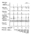
present embodiment. Figs. 3(a)-3(h) are timing charts
showing the operations of the optical measurement apparatus
according to the present embodiment. It is noted that three
photons impinge on the HPD 24 59 ns after the measurement
start time (t=0), five photons impinge on the HPD 24 120 ns
after the measurement start time, four photons impinge on
the HPD 24 181 ns after the measurement start time, one
photon impinges on the HPD 24 245 ns after the measurement
start time, and two photons impinge on the HPD 24 282 ns
after the measurement start time, as shown in Fig. 3(a).
At the start of the measurements, the CPU 18 outputs a
reset signal to the counter 34 to reset the counter 34.
After being reset, the counter 34 begins counting pulse
signals received from the timer 32.
Since output from the HPD 24 and TZ amplifier 26 are
small until photons are detected by the HPD 24, that is,
from the measurement start time until 59 ns have elapsed,
and the output from the peak holding circuit 28 does not
exceed the reference voltage, the delay circuit 37 does not
output a trigger signal and data is not stored in the memory
38.
However, when 3 photons impinge on the HPD 24 after 59
ns have elapsed from the measurement start time,
photoelectrons are emitted from the photocathode 24a and
multiplied by the APD 24b. The current outputted from the
HPD 24 is converted to a voltage by the TZ amplifier 26. A
waveform indicating the peak voltage of about 0.75 V,
equivalent to 3 photons, is outputted, as shown in Fig. 3(b).
More specifically, the peak holding circuit 28 detects
an output signal from the TZ amplifier 26, and this
detection result is outputted to the A/D converter 30 and
comparator 36 (Fig. 3(c)). When the output signal from the
TZ amplifier 26 reaches a peak value, this peak value is
saved for a prescribed interval by the peak holding circuit
28 and continuously outputted to the A/D converter 30 and
comparator 36 (Fig. 3(c)).
When the output signal from the TZ amplifier 26 is
greater than the reference voltage (0.13 V) inputted into
the comparator 36, the output from the comparator 36 is set
to high level. After the delay circuit 37 applies the
prescribed delay 1, this high level output is outputted as a
trigger signal to the A/D converter 30 and memory 38 (Fig.
3(d)). When a trigger signal is inputted into the A/D
converter 30 from the delay circuit 37 in this way, the A/D
converter 30 performs A/D conversion on the signal inputted
from the peak holding circuit 28. The delay 1 is set
equivalent to or slightly longer than the time required for
the output waveform from the TZ amplifier 26 to travel from
0 V to the peak voltage. Accordingly, the peak value of the
output signal from the TZ amplifier 26 of about 0.75 V
(equivalent to 3 photons) is inputted into the A/D converter
30 at the instant when a trigger signal is inputted into the
A/D converter 30. Therefore, the digital value "3" is
outputted from the A/D converter 30, as shown in Fig. 3(f).
Since the trigger signal is inputted also into the
memory 38 from the delay circuit 37, the output value from
the A/D converter 30 and the time signal outputted from the
counter 34, as shown in Fig. 3(g), are stored in the memory
38. In other words, the value of a time signal, which is
inputted from the counter 34 first after a trigger signal
has been inputted into the memory 38, is stored in the
memory 38.
It is noted that reset signals are outputted from the
counter 34 to the peak holding circuit 28 repeatedly at the
fixed time interval (for example 5 ns), as shown in Fig.
3(e). Accordingly, the output signal of the peak holding
circuit 28 is reset repeatedly at the fixed time interval
(for example, 5 ns), as shown in Fig. 3(c).
Similarly, when photons fall incident on the HPD 24,
the number of incident photons and the time signal at the
photon-incident time are stored in the memory 38. As a
result, the data stored in the memory 38 is similar to that
shown in Fig. 3(h).
As described above, the optical measurement apparatus
10 primarily includes the photon detection unit 12 for
detecting incident photons, the time signal output unit 14
for outputting time signals, and the storage unit 16 for
storing time signals that are outputted from the time signal
output unit 14 when the photon detection unit 12 detects
photons. The photon detection unit 12 includes the HPD 24
having the photocathode 24a and APD 24b, the TZ amplifier 26,
the peak holding circuit 28, and the A/D converter 30. The
time signal output unit 14 includes the timer 32 and counter
34. The storage unit 16 includes the comparator 36, delay
circuit 37 for A/D conversion, and memory 38. When photons
impinge on the HPD 24, the delay circuit 37 outputs a
trigger signal, triggering the photon-number, outputted from
the A/D converter 30, along with the time data outputted
from the counter 34 to be stored in the memory 38.
Next, the operations and effects of the optical
measurement apparatus according to the present embodiment
will be described. By storing the number of photons
detected by the HPD 24 and the time signal outputted from
the counter 34 in the memory 38 when photons are detected,
the optical measurement apparatus 10 of the present
embodiment can measure when and how many photons have
arrived. However, since no data is stored in the memory 38
when the HPD 24 does not detect photons, the amount of data
stored therein is extremely small. Therefore, the capacity
of the memory 38 can be used effectively, and the optical
measurement apparatus 10 can measure, over a long period of
time, when and how many photons have arrived.
Let us take a specific example of incident photons
having a time series distribution as shown in Fig. 4(a).
When using a digital oscilloscope to measure when and how
many photons have arrived, data for 256 gradations (8 bits)
of the output value is stored in memory every 1 ns along the
time axis shown in Fig. 4(b). In contrast, when using the
optical measurement apparatus 10 of the present embodiment,
as shown in Fig. 4(c), only when photons impinge on the HPD
24, only the number of photons of a maximum of four
gradations (2 bits) and the time data at that instant need
be stored. In other words, by using the optical measurement
apparatus 10 of the present embodiment with a 64-MB memory,
it is possible to measure and record up to a maximum of 16
million events (incidence of photons), during the measuring
time of 150 seconds, with the time resolution of 5 ns. By
further employing the external memory 20, it is possible to
measure and record for an even longer time.
Further, in the optical measurement apparatus 10 of
the present embodiment, the A/D converter 30 outputs the
number of incident photons as a digital value. Accordingly,
signals outputted from the A/D converter 30 can be directly
stored in the memory 38 and directly displayed on the
display unit 22.
The optical measurement apparatus 10 according to the
present embodiment employs the HPD 24 provided with the
photocathode 24a and APD 24b, making it possible to
efficiently detect the number of photons that impinge on the
HPD 24 simultaneously (or at extremely close timings).
In the optical measurement apparatus 10 of the present
embodiment, the HPD 24 is used as the photodetector.
However, it is possible to use a VLPC (visual light photon
counter) or the like, as well. The VLPC is formed of an
arsenic-doped silicon substrate and a thin, non-doped
epitaxial layer on the silicon substrate. Avalanche
multiplication is generated by cooling the VLPC to about 7 K
and applying about 7 V thereto, obtaining a gain of about 5
X 104. Such a high gain can be obtained using VLPC because
the band gap can be considered as equivalent to the
ionization energy produced from the impurity level. By
obtaining such a high gain, the VLPC, like the HPD, can
differentiate and output the number of incident photons.
The following variations are conceivable for the
optical measurement apparatus 10 according to the present
embodiment.
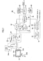
An optical measurement apparatus 50 according to a
first variation will be described with reference to Fig. 5.
Rather than outputting a reset signal to the peak
holding circuit 28 from the counter 34, the optical
measurement apparatus 50 is provided with a delay circuit 29
for outputting a reset signal to the peak holding circuit 28.
A trigger signal outputted from the delay circuit 37 is
inputted into the delay circuit 29.
With this construction, when photons impinge on the
HPD 24, the input voltage of the comparator 36 becomes
larger than the reference voltage, causing a trigger signal
to be outputted from the delay circuit 37. Upon receiving
this trigger signal, the A/D converter 30 converts the
output signal from the peak holding circuit 28 from analog
to digital and outputs the converted result to the memory 38.
The memory 38, having received the same trigger signal,
stores the output signal from the A/D converter 30 and the
time signal from the counter 34. Further, after being
applied with a prescribed delay 2 by the delay circuit 29,
the trigger signal is outputted to the peak holding circuit
28 as a reset signal. Accordingly, the peak holding circuit
28 is reset after a fixed time has elapsed since the trigger
signal has been outputted from the delay circuit 37.
Fig. 6(a)-6(h) are timing charts showing the
operations of the optical measurement apparatus 50. The
point, at which the operations of the optical measurement
apparatus 50 differ from those of the optical measurement
apparatus 10 according to the embodiment described above, is
that the peak holding circuit 28 is reset in response to a
trigger signal generated by the delay circuit 37, that is,
in response to incidence of photons. This reset signal is
generated by delaying the trigger signal from the delay
circuit 37 a fixed delay 2 with the delay circuit 29.
Accordingly, the peak holding circuit 28 is reset after the
A/D converter 30 performs A/D conversion. With this
construction, even when a plurality of photons impinge
sequentially within a period that is equal to the reset
interval set in the optical measurement apparatus 10 in the
embodiment described above, the optical measurement
apparatus 50 can record the number of photons at each
photon-incident event and the time of each photon-incident
event.
Fig. 7 shows the construction of an optical
measurement apparatus 60 according to a second variation of
the preferred embodiment. In the optical measurement
apparatus 10 of the preferred embodiment described above,
the current signal outputted from the HPD 24 is converted to
a voltage by the TZ amplifier 26, and the peak holding
circuit 28 outputs an output signal that is resulted by
holding the peak value for the fixed time period. However,
these functions can be achieved by a charge amplifier 40
with reset function, as in the optical measurement apparatus
60 of the present variation. The charge amplifier 40
includes an operational amplifier 40a, a capacitor 40b, and
a reset switch 40c. A first input terminal of the
operational amplifier 40a is grounded, and the output
current from the HPD 24 is inputted into a second input
terminal. The output terminal of the operational amplifier
40a is connected to the input terminal of the A/D converter
30 and the plus input terminal of the comparator 36. The
capacitor 40b is connected to the second input terminal of
the operational amplifier 40a and the output terminal of the
operational amplifier 40a. The reset switch 40c is
connected in parallel with the capacitor 40b. The charge
amplifier 40 integrates the electrical charge outputted from
the HPD 24 and outputs the voltage resulting from the
integration, and is reset when the reset switch 40c is
turned ON by a reset signal outputted from the counter 34
(reset signal A in Fig. 7).
The comparator 36 compares the output voltage from the
charge amplifier 40 to a reference voltage and switches its
logical output to the high level when the output voltage is
greater than the reference voltage and to the low level when
the output level is smaller than the reference voltage. The
high level logic output is outputted as a trigger signal.
Figs. 8(a)-8(h) are timing charts. The counter 34 in
the time signal output unit 14 of the optical measurement
apparatus 60 outputs a read signal (read signal C in Fig. 7)
just prior to outputting a reset signal (Figs. 8(b) and
8(c)).
An AND circuit 42 is provided downstream from the
comparator 36 in the storage unit 16. The read signal
outputted from the counter 34 and the trigger signal
outputted from the comparator 36 (Fig. 8(e)) are inputted
into the AND circuit 42. The AND circuit 42 outputs an
output signal to the A/D converter 30 and the memory 38.
Accordingly, the A/D converter 30 performs A/D conversion at
the instant when the read signal is outputted from the
counter 34 after the output voltage from the charge
amplifier 40 (Fig. 8(d)) exceeds the reference voltage. The
output signal from the A/D converter 30 is stored along with
the time signal from the counter 34 in the memory 38. This
construction eliminates the need for providing the peak
holding circuit 28 and the delay circuit 37 of the
embodiment described above. Further, the optical
measurement apparatus 60 can minimize errors when a
plurality of photons are continuously impinged within a
short time.
In the optical measurement apparatus 10 of the
embodiment described above, the counter 34 is reset by a
reset signal outputted from the CPU 18 at the beginning of a
measurement. However, the counter 34 can be reset by the
trigger signal from the delay circuit 37, as in an optical
measurement apparatus 70 according to a third variation
shown in Fig. 9. With this construction, by resetting the
counter 34 in time with the incidence of photons, the time
signal outputted from the counter 34 indicates the time
interval at which photons fall incident on the HPD 24
successively. Accordingly, the number of photons falling
incident on the HPD 24 and the time interval at which the
photons fall incident on the HPD 24 are stored in the memory
38.
Further, while the optical measurement apparatus 10
according to the embodiment described above employs the APD
24b as the semiconductor photodetector, a photodiode or the
like can also be used.
The optical measurement apparatus and method for
optical measurement of the present invention are not limited
to the embodiments described above. Many modifications and
variations may be made therein.
For example, a time signal, which is inputted from the
counter 34 at the first time after the trigger signal has
been inputted into the memory 38, is stored in the memory 38
in the optical measurement apparatus and method for optical
measurement of the preferred embodiment. However, it is
also possible to store in the memory 38 the last time signal
that has been inputted from the counter 34 prior to the time
when the trigger signal is inputted into the memory 38.
The optical measurement apparatus and method for
optical measurement according to the present invention are
widely used in the detection of bioluminescence.
Claims (14)
- An optical measurement apparatus, comprising:a photon detecting portion detecting incident photons;a time signal outputting portion outputting time signals; anda storing portion storing a time signal that is outputted from the time signal outputting portion at the time when the photon detecting portion detects photons.
- An optical measurement apparatus as claimed in claim 1, wherein the photon detecting portion detects the number of the incident photons, and
wherein the storing portion stores, when the photon detecting portion detects photons, both the number of photons detected by the photon detecting portion and the time signal outputted by the time signal outputting portion. - An optical measurement apparatus as claimed in claim 2, wherein the photon detecting portion includes an analog-to-digital converter outputting the number of the incident photons in a digital value.
- An optical measurement apparatus as claimed in Claim 2, wherein the photon detecting portion includes:a photocathode emitting photoelectrons that correspond to the number of the incident photons;an accelerating portion accelerating the photoelectrons emitted from the photocathode; anda semiconductor photodetector receiving the photoelectrons accelerated by the accelerating portion and outputting an output signal that corresponds to the number of the photoelectrons.
- An optical measurement apparatus as claimed in Claim 4, wherein the semiconductor photodetector includes an avalanche photodiode.
- An optical measurement apparatus as claimed in claim 1, wherein the photon detecting portion outputs a detection signal indicative of a detection result,
wherein the time signal outputting portion outputs the time signal repeatedly at a fixed time interval, and
wherein the storing portion includes a comparing portion that compares the detection signal to a predetermined threshold value and that outputs a trigger signal when the detection signal is larger than the threshold value; anda storage controlling portion storing a time signal upon receipt of the trigger signal. - An optical measurement apparatus as claimed in claim 3,
wherein the photon detecting portion outputs a detection signal indicative of the number of the detected photons,
wherein the time signal outputting portion outputs a time signal repeatedly at a fixed time interval;
wherein the storing portion includes a comparing portion comparing the detection signal to a predetermined threshold value and outputting a trigger signal when the detection signal is larger than the threshold value, the analog-to-digital converter converting the detection signal, supplied from the photon detecting portion, into a digital value upon receipt of the trigger signal, and
wherein the storing portion further includes a storage controlling portion storing the digital value and the time signal in response to the trigger signal. - An optical measurement apparatus as claimed in claim 7,
wherein the photon detecting portion includes:wherein the comparing portion compares a detection result of the detecting operation performed by the output signal detector to the predetermined threshold value, the comparing portion outputting a trigger signal when the detection result is larger than the threshold value.a photodetector outputting an output signal that corresponds to the number of the incident photons, andan output signal detector repeatedly performing a detection operation for detecting the output signal for a predetermined time period, - An optical measurement apparatus as claimed in claim 8, wherein the output signal detector includes a peak holding circuit detecting the output signal supplied from the photodetector and holding a peak thereof,
wherein the comparing portion compares the output signal detected by the peak holding circuit with the threshold value and outputs a trigger signal when a predetermined delay time has elapsed after the output signal has become larger than the threshold value, thereby causing the analog-to-digital converter to convert the peak value to a digital value. - An optical measurement apparatus as claimed in claim 9, wherein the time signal outputting portion repeatedly outputs a reset signal at a predetermined time interval, to thereby cause the peak detector to be reset in response to the reset signal.
- An optical measurement apparatus as claimed in claim 9, wherein the comparing portion resets the peak detector by outputting a reset signal to the peak detector when a predetermined time has elapsed after the comparing portion outputs the trigger signal.
- An optical measurement apparatus as claimed in claim 8, wherein the photodetector outputs an electric current signal that corresponds to the number of the incident photons,
wherein the output signal detector includes an integrating portion converting the electric current signal to an electric voltage signal by integrating the electric current signal,
wherein the time signal outputting portion repeatedly outputs a pair of read signal and a reset signal at a predetermined interval, the time signal outputting portion outputting the pair of a read signal and a reset signal by outputting the read signal and the reset signal in this order,
wherein the integrating portion is reset in response to the reset signal, and
wherein the comparing portion compares the voltage signal to the predetermined threshold value, and outputs a trigger signal if the voltage signal is larger than the threshold value at the time when the comparing portion receives the read signal. - An optical measurement method, comprising:a photon detecting step detecting incident photons;a time signal outputting step outputting time signals; anda storing step storing a time signal that is outputted from the time signal outputting step at the time when the photon detecting step detects photons.
- An optical measurement method as claimed in claim 13, wherein the photodetecting step detects a plurality of incident photons in separation from one another,
wherein the storing step stores, when the photon detecting step detects photons, both the number of photons detected by the photon detecting step and the time signal outputted by the time signal outputting step.
Applications Claiming Priority (1)
| Application Number | Priority Date | Filing Date | Title |
|---|---|---|---|
| PCT/JP2000/006562 WO2002027284A1 (en) | 2000-09-25 | 2000-09-25 | Optical measurement apparatus and method for optical measurement |
Publications (2)
| Publication Number | Publication Date |
|---|---|
| EP1329700A1 true EP1329700A1 (en) | 2003-07-23 |
| EP1329700A4 EP1329700A4 (en) | 2011-03-23 |
Family
ID=11736511
Family Applications (1)
| Application Number | Title | Priority Date | Filing Date |
|---|---|---|---|
| EP00962814A Withdrawn EP1329700A4 (en) | 2000-09-25 | 2000-09-25 | Optical measurement apparatus and method for optical measurement |
Country Status (4)
| Country | Link |
|---|---|
| US (1) | US6940589B1 (en) |
| EP (1) | EP1329700A4 (en) |
| AU (1) | AU2000274441A1 (en) |
| WO (1) | WO2002027284A1 (en) |
Cited By (6)
| Publication number | Priority date | Publication date | Assignee | Title |
|---|---|---|---|---|
| EP1770985A3 (en) * | 2005-07-18 | 2007-12-05 | Neuricam S.P.A. | Photo-sensitive element for electro-optical sensors |
| WO2008054883A3 (en) * | 2006-06-07 | 2008-10-16 | Xrf Corp | Devices and methods for detecting and analyzing radiation |
| WO2008080083A3 (en) * | 2006-12-22 | 2009-03-05 | Univ Washington | High performance imaging system for diffuse optical tomography and associated method of use |
| CN106052861A (en) * | 2016-07-27 | 2016-10-26 | 武汉京邦科技有限公司 | Silicon photomultiplier test system and test method |
| US9480425B2 (en) | 2008-04-17 | 2016-11-01 | Washington University | Task-less optical mapping of dynamic brain function using resting state functional connectivity |
| CN106949979A (en) * | 2017-02-09 | 2017-07-14 | 北京建筑大学 | A kind of light velocity measurement method based on LC oscillating circuits |
Families Citing this family (7)
| Publication number | Priority date | Publication date | Assignee | Title |
|---|---|---|---|---|
| GB2398118B (en) * | 2003-02-07 | 2006-03-15 | Imp College Innovations Ltd | Photon arrival time detection |
| US7858917B2 (en) * | 2003-05-02 | 2010-12-28 | Massachusetts Institute Of Technology | Digital photon-counting geiger-mode avalanche photodiode solid-state monolithic intensity imaging focal-plane with scalable readout circuitry |
| JP5494063B2 (en) * | 2010-03-17 | 2014-05-14 | コニカミノルタ株式会社 | Control device and image forming apparatus |
| FR3058230B1 (en) * | 2016-10-27 | 2019-03-15 | Detection Technology Sas | SPECTROMETRY DEVICE |
| US10852399B2 (en) * | 2018-03-30 | 2020-12-01 | Tower Semiconductor Ltd. | Active quenching for single-photon avalanche diode using one- shot circuit |
| ES2962472T3 (en) * | 2020-06-26 | 2024-03-19 | Alpsentek Gmbh | Delta image sensor with digital pixel storage |
| CN119688093B (en) * | 2024-12-13 | 2025-09-30 | 季华实验室 | Single-photon detector performance parameter measurement method, device, equipment and medium |
Family Cites Families (14)
| Publication number | Priority date | Publication date | Assignee | Title |
|---|---|---|---|---|
| JPS63184073A (en) * | 1986-07-23 | 1988-07-29 | Shimadzu Corp | Peak value detection circuit |
| JP3413241B2 (en) | 1993-05-07 | 2003-06-03 | 浜松ホトニクス株式会社 | Electron tube |
| US5349193A (en) * | 1993-05-20 | 1994-09-20 | Princeton Gamma Tech, Inc. | Highly sensitive nuclear spectrometer apparatus and method |
| JPH08148113A (en) * | 1994-11-24 | 1996-06-07 | Hamamatsu Photonics Kk | Photomultiplier tube |
| FR2738919B1 (en) * | 1995-09-15 | 1997-10-17 | Commissariat Energie Atomique | METHOD AND DEVICE FOR THE CORRECTION OF SPECTROMETRIC MEASUREMENT IN THE FIELD OF GAMMA PHOTON DETECTION |
| JPH09196752A (en) * | 1995-11-15 | 1997-07-31 | Bunshi Bio Photonics Kenkyusho:Kk | Photometric device |
| JPH09189604A (en) * | 1996-01-11 | 1997-07-22 | Hamamatsu Photonics Kk | Method for determining counting prohibition time and photon counting device |
| JPH09297055A (en) | 1996-05-02 | 1997-11-18 | Hamamatsu Photonics Kk | Electron tube |
| JPH09312145A (en) | 1996-05-23 | 1997-12-02 | Hamamatsu Photonics Kk | Electron tube |
| JPH10300573A (en) * | 1997-04-30 | 1998-11-13 | Asahi Optical Co Ltd | Light intensity measurement device |
| JP3742490B2 (en) | 1997-07-22 | 2006-02-01 | 浜松ホトニクス株式会社 | Optical waveform measuring device |
| JP3742491B2 (en) * | 1997-07-22 | 2006-02-01 | 浜松ホトニクス株式会社 | Optical waveform measuring device |
| US6189221B1 (en) * | 1998-12-31 | 2001-02-20 | The Rival Company | Can opener appliance having a side-cutting mechanism |
| JP2000275101A (en) * | 1999-03-26 | 2000-10-06 | Hamamatsu Photonics Kk | Optical measuring device and optical measuring method |
-
2000
- 2000-09-25 WO PCT/JP2000/006562 patent/WO2002027284A1/en not_active Ceased
- 2000-09-25 AU AU2000274441A patent/AU2000274441A1/en not_active Abandoned
- 2000-09-25 EP EP00962814A patent/EP1329700A4/en not_active Withdrawn
- 2000-09-25 US US10/381,370 patent/US6940589B1/en not_active Expired - Fee Related
Cited By (9)
| Publication number | Priority date | Publication date | Assignee | Title |
|---|---|---|---|---|
| EP1770985A3 (en) * | 2005-07-18 | 2007-12-05 | Neuricam S.P.A. | Photo-sensitive element for electro-optical sensors |
| WO2008054883A3 (en) * | 2006-06-07 | 2008-10-16 | Xrf Corp | Devices and methods for detecting and analyzing radiation |
| US7576326B2 (en) | 2006-06-07 | 2009-08-18 | Xrf Corporation | Devices and methods for detecting and analyzing radiation |
| WO2008080083A3 (en) * | 2006-12-22 | 2009-03-05 | Univ Washington | High performance imaging system for diffuse optical tomography and associated method of use |
| US7983740B2 (en) | 2006-12-22 | 2011-07-19 | Washington University | High performance imaging system for diffuse optical tomography and associated method of use |
| US9480425B2 (en) | 2008-04-17 | 2016-11-01 | Washington University | Task-less optical mapping of dynamic brain function using resting state functional connectivity |
| CN106052861A (en) * | 2016-07-27 | 2016-10-26 | 武汉京邦科技有限公司 | Silicon photomultiplier test system and test method |
| CN106052861B (en) * | 2016-07-27 | 2017-08-29 | 武汉京邦科技有限公司 | A kind of silicon photoelectric multiplier test system and method for testing |
| CN106949979A (en) * | 2017-02-09 | 2017-07-14 | 北京建筑大学 | A kind of light velocity measurement method based on LC oscillating circuits |
Also Published As
| Publication number | Publication date |
|---|---|
| AU2000274441A1 (en) | 2002-04-08 |
| EP1329700A4 (en) | 2011-03-23 |
| WO2002027284A1 (en) | 2002-04-04 |
| US6940589B1 (en) | 2005-09-06 |
Similar Documents
| Publication | Publication Date | Title |
|---|---|---|
| CN211554305U (en) | LiDAR readout circuit | |
| KR102526443B1 (en) | Histogram reading method and circuit for determining photon time-of-flight | |
| US6940589B1 (en) | Optical measurement apparatus and method for optical measurement | |
| US8581172B2 (en) | High-speed analog photon counter and method | |
| US8859944B2 (en) | Coordinated in-pixel light detection method and apparatus | |
| US5715049A (en) | Light measuring apparatus for quantifying photons | |
| EP2041769A2 (en) | Method and device for detecting weak optical signals | |
| WO2004070419A1 (en) | Photon arrival time detection | |
| US6960771B1 (en) | Optical measurement apparatus and method for optical measurement | |
| JP4183849B2 (en) | Optical measuring device | |
| JP3742491B2 (en) | Optical waveform measuring device | |
| US5694211A (en) | Light measuring apparatus for quantizing photon | |
| US7135669B2 (en) | Low-level light detector and low-level light imaging apparatus | |
| JPH1137850A (en) | Optical waveform measurement device | |
| Boutot et al. | Impulse response of curved microchannel plate photomultipliers | |
| JP2000275101A (en) | Optical measuring device and optical measuring method | |
| JP2658843B2 (en) | Single photon measuring device | |
| JP2005207955A (en) | Circuit for photodetection, and photodetector | |
| EP1329699A1 (en) | Optical measurement apparatus and method for optical measurement | |
| JP2001027567A (en) | Optical measurement device | |
| US20180259391A1 (en) | Coincidence resolving time readout circuit | |
| US4985628A (en) | Inspection apparatus incorporating digital electron detection | |
| Sun et al. | Photon counting performance measurements of transfer electron InGaAsP photocathode hybrid photomultiplier tubes at 1064 nm wavelength | |
| Lopez-Delgado et al. | Measuring the length and the time structure of the electron bunch in electron storage rings by single photon timing | |
| Kalytis | Photon Counting in Astrophotometry. Fundamentals and Some Advices for Beginners |
Legal Events
| Date | Code | Title | Description |
|---|---|---|---|
| PUAI | Public reference made under article 153(3) epc to a published international application that has entered the european phase |
Free format text: ORIGINAL CODE: 0009012 |
|
| 17P | Request for examination filed |
Effective date: 20030415 |
|
| AK | Designated contracting states |
Designated state(s): AT BE CH CY DE DK ES FI FR GB GR IE IT LI LU MC NL PT SE |
|
| AX | Request for extension of the european patent |
Extension state: AL LT LV MK RO SI |
|
| RBV | Designated contracting states (corrected) |
Designated state(s): DE FR GB |
|
| A4 | Supplementary search report drawn up and despatched |
Effective date: 20110223 |
|
| STAA | Information on the status of an ep patent application or granted ep patent |
Free format text: STATUS: THE APPLICATION IS DEEMED TO BE WITHDRAWN |
|
| 18D | Application deemed to be withdrawn |
Effective date: 20110525 |