EP1329474A1 - Polythiophenes and devices thereof - Google Patents
Polythiophenes and devices thereof Download PDFInfo
- Publication number
- EP1329474A1 EP1329474A1 EP03000412A EP03000412A EP1329474A1 EP 1329474 A1 EP1329474 A1 EP 1329474A1 EP 03000412 A EP03000412 A EP 03000412A EP 03000412 A EP03000412 A EP 03000412A EP 1329474 A1 EP1329474 A1 EP 1329474A1
- Authority
- EP
- European Patent Office
- Prior art keywords
- accordance
- group
- polythiophene
- polythiophenes
- thin film
- Prior art date
- Legal status (The legal status is an assumption and is not a legal conclusion. Google has not performed a legal analysis and makes no representation as to the accuracy of the status listed.)
- Granted
Links
- 229920000123 polythiophene Polymers 0.000 title claims abstract description 77
- 238000006116 polymerization reaction Methods 0.000 claims abstract description 10
- 125000005556 thienylene group Chemical group 0.000 claims abstract description 9
- 239000010409 thin film Substances 0.000 claims description 40
- -1 oligoarylene Chemical group 0.000 claims description 31
- 239000004065 semiconductor Substances 0.000 claims description 28
- 239000000758 substrate Substances 0.000 claims description 17
- 125000000217 alkyl group Chemical group 0.000 claims description 12
- 125000000732 arylene group Chemical group 0.000 claims description 10
- 125000004432 carbon atom Chemical group C* 0.000 claims description 9
- 125000002529 biphenylenyl group Chemical group C1(=CC=CC=2C3=CC=CC=C3C12)* 0.000 claims description 8
- 125000005567 fluorenylene group Chemical group 0.000 claims description 8
- 125000000843 phenylene group Chemical group C1(=C(C=CC=C1)*)* 0.000 claims description 8
- 239000004793 Polystyrene Substances 0.000 claims description 7
- 229920002223 polystyrene Polymers 0.000 claims description 7
- SNRUBQQJIBEYMU-UHFFFAOYSA-N Dodecane Natural products CCCCCCCCCCCC SNRUBQQJIBEYMU-UHFFFAOYSA-N 0.000 claims description 5
- 125000002704 decyl group Chemical group [H]C([H])([H])C([H])([H])C([H])([H])C([H])([H])C([H])([H])C([H])([H])C([H])([H])C([H])([H])C([H])([H])C([H])([H])* 0.000 claims description 5
- 125000003438 dodecyl group Chemical group [H]C([H])([H])C([H])([H])C([H])([H])C([H])([H])C([H])([H])C([H])([H])C([H])([H])C([H])([H])C([H])([H])C([H])([H])C([H])([H])C([H])([H])* 0.000 claims description 5
- 125000003187 heptyl group Chemical group [H]C([*])([H])C([H])([H])C([H])([H])C([H])([H])C([H])([H])C([H])([H])C([H])([H])[H] 0.000 claims description 5
- 125000004051 hexyl group Chemical group [H]C([H])([H])C([H])([H])C([H])([H])C([H])([H])C([H])([H])C([H])([H])* 0.000 claims description 5
- 125000000325 methylidene group Chemical group [H]C([H])=* 0.000 claims description 5
- 125000001400 nonyl group Chemical group [H]C([*])([H])C([H])([H])C([H])([H])C([H])([H])C([H])([H])C([H])([H])C([H])([H])C([H])([H])C([H])([H])[H] 0.000 claims description 5
- 125000002347 octyl group Chemical group [H]C([*])([H])C([H])([H])C([H])([H])C([H])([H])C([H])([H])C([H])([H])C([H])([H])C([H])([H])[H] 0.000 claims description 5
- 125000005560 phenanthrenylene group Chemical group 0.000 claims description 5
- 125000002948 undecyl group Chemical group [H]C([*])([H])C([H])([H])C([H])([H])C([H])([H])C([H])([H])C([H])([H])C([H])([H])C([H])([H])C([H])([H])C([H])([H])C([H])([H])[H] 0.000 claims description 5
- 239000004721 Polyphenylene oxide Substances 0.000 claims description 4
- 125000004183 alkoxy alkyl group Chemical group 0.000 claims description 4
- 238000005227 gel permeation chromatography Methods 0.000 claims description 4
- 125000001421 myristyl group Chemical group [H]C([*])([H])C([H])([H])C([H])([H])C([H])([H])C([H])([H])C([H])([H])C([H])([H])C([H])([H])C([H])([H])C([H])([H])C([H])([H])C([H])([H])C([H])([H])C([H])([H])[H] 0.000 claims description 4
- 125000002958 pentadecyl group Chemical group [H]C([*])([H])C([H])([H])C([H])([H])C([H])([H])C([H])([H])C([H])([H])C([H])([H])C([H])([H])C([H])([H])C([H])([H])C([H])([H])C([H])([H])C([H])([H])C([H])([H])C([H])([H])[H] 0.000 claims description 4
- 125000005010 perfluoroalkyl group Chemical group 0.000 claims description 4
- 229920000570 polyether Polymers 0.000 claims description 4
- 125000002889 tridecyl group Chemical group [H]C([*])([H])C([H])([H])C([H])([H])C([H])([H])C([H])([H])C([H])([H])C([H])([H])C([H])([H])C([H])([H])C([H])([H])C([H])([H])C([H])([H])C([H])([H])[H] 0.000 claims description 4
- 125000000484 butyl group Chemical group [H]C([*])([H])C([H])([H])C([H])([H])C([H])([H])[H] 0.000 claims description 3
- 125000001147 pentyl group Chemical group C(CCCC)* 0.000 claims description 3
- 125000001436 propyl group Chemical group [H]C([*])([H])C([H])([H])C([H])([H])[H] 0.000 claims description 2
- 125000000547 substituted alkyl group Chemical group 0.000 claims description 2
- 239000010410 layer Substances 0.000 description 53
- WYURNTSHIVDZCO-UHFFFAOYSA-N Tetrahydrofuran Chemical compound C1CCOC1 WYURNTSHIVDZCO-UHFFFAOYSA-N 0.000 description 22
- 239000000243 solution Substances 0.000 description 22
- OKKJLVBELUTLKV-UHFFFAOYSA-N Methanol Chemical compound OC OKKJLVBELUTLKV-UHFFFAOYSA-N 0.000 description 21
- YMWUJEATGCHHMB-UHFFFAOYSA-N Dichloromethane Chemical compound ClCCl YMWUJEATGCHHMB-UHFFFAOYSA-N 0.000 description 18
- HEDRZPFGACZZDS-MICDWDOJSA-N Trichloro(2H)methane Chemical compound [2H]C(Cl)(Cl)Cl HEDRZPFGACZZDS-MICDWDOJSA-N 0.000 description 16
- 238000000034 method Methods 0.000 description 14
- 239000000463 material Substances 0.000 description 13
- 229920000642 polymer Polymers 0.000 description 13
- 238000004519 manufacturing process Methods 0.000 description 12
- YLQBMQCUIZJEEH-UHFFFAOYSA-N tetrahydrofuran Natural products C=1C=COC=1 YLQBMQCUIZJEEH-UHFFFAOYSA-N 0.000 description 11
- 239000000203 mixture Substances 0.000 description 10
- PXHVJJICTQNCMI-UHFFFAOYSA-N Nickel Chemical compound [Ni] PXHVJJICTQNCMI-UHFFFAOYSA-N 0.000 description 9
- YXFVVABEGXRONW-UHFFFAOYSA-N Toluene Chemical compound CC1=CC=CC=C1 YXFVVABEGXRONW-UHFFFAOYSA-N 0.000 description 9
- 238000004528 spin coating Methods 0.000 description 9
- VYPSYNLAJGMNEJ-UHFFFAOYSA-N Silicium dioxide Chemical compound O=[Si]=O VYPSYNLAJGMNEJ-UHFFFAOYSA-N 0.000 description 8
- XUIMIQQOPSSXEZ-UHFFFAOYSA-N Silicon Chemical compound [Si] XUIMIQQOPSSXEZ-UHFFFAOYSA-N 0.000 description 8
- QVGXLLKOCUKJST-UHFFFAOYSA-N atomic oxygen Chemical compound [O] QVGXLLKOCUKJST-UHFFFAOYSA-N 0.000 description 8
- MVPPADPHJFYWMZ-UHFFFAOYSA-N chlorobenzene Chemical compound ClC1=CC=CC=C1 MVPPADPHJFYWMZ-UHFFFAOYSA-N 0.000 description 8
- 239000010408 film Substances 0.000 description 8
- 239000000178 monomer Substances 0.000 description 8
- VLKZOEOYAKHREP-UHFFFAOYSA-N n-Hexane Chemical compound CCCCCC VLKZOEOYAKHREP-UHFFFAOYSA-N 0.000 description 8
- 229910052760 oxygen Inorganic materials 0.000 description 8
- 239000001301 oxygen Substances 0.000 description 8
- 230000008569 process Effects 0.000 description 8
- 229910052710 silicon Inorganic materials 0.000 description 8
- 239000010703 silicon Substances 0.000 description 8
- 239000002904 solvent Substances 0.000 description 8
- VEXZGXHMUGYJMC-UHFFFAOYSA-N Hydrochloric acid Chemical compound Cl VEXZGXHMUGYJMC-UHFFFAOYSA-N 0.000 description 7
- YNZKCHBXBASBJT-UHFFFAOYSA-N 3,4-dioctyl-2,5-dithiophen-2-ylthiophene Chemical compound CCCCCCCCC=1C(CCCCCCCC)=C(C=2SC=CC=2)SC=1C1=CC=CS1 YNZKCHBXBASBJT-UHFFFAOYSA-N 0.000 description 6
- 0 CC(C)(C)c1ccc(-c2c(C)c(*)c(-c3ccc(C(C)(C)C)[s]3)[s]2)[s]1 Chemical compound CC(C)(C)c1ccc(-c2c(C)c(*)c(-c3ccc(C(C)(C)C)[s]3)[s]2)[s]1 0.000 description 6
- RTZKZFJDLAIYFH-UHFFFAOYSA-N Diethyl ether Chemical compound CCOCC RTZKZFJDLAIYFH-UHFFFAOYSA-N 0.000 description 6
- 229920001940 conductive polymer Polymers 0.000 description 6
- 238000011156 evaluation Methods 0.000 description 6
- PCHJSUWPFVWCPO-UHFFFAOYSA-N gold Chemical compound [Au] PCHJSUWPFVWCPO-UHFFFAOYSA-N 0.000 description 6
- 229910052737 gold Inorganic materials 0.000 description 6
- 239000010931 gold Substances 0.000 description 6
- 239000000976 ink Substances 0.000 description 6
- 229910052751 metal Inorganic materials 0.000 description 6
- 239000002184 metal Substances 0.000 description 6
- 238000007639 printing Methods 0.000 description 6
- 239000011541 reaction mixture Substances 0.000 description 6
- 229910052814 silicon oxide Inorganic materials 0.000 description 6
- XLYOFNOQVPJJNP-UHFFFAOYSA-N water Substances O XLYOFNOQVPJJNP-UHFFFAOYSA-N 0.000 description 6
- 238000005160 1H NMR spectroscopy Methods 0.000 description 5
- 238000006243 chemical reaction Methods 0.000 description 5
- 239000011521 glass Substances 0.000 description 5
- 230000001590 oxidative effect Effects 0.000 description 5
- 238000002360 preparation method Methods 0.000 description 5
- 239000000725 suspension Substances 0.000 description 5
- 238000012360 testing method Methods 0.000 description 5
- BNXJIUWYGDXAOL-UHFFFAOYSA-N 2,5-bis(5-bromothiophen-2-yl)-3,4-dioctylthiophene Chemical compound CCCCCCCCC=1C(CCCCCCCC)=C(C=2SC(Br)=CC=2)SC=1C1=CC=C(Br)S1 BNXJIUWYGDXAOL-UHFFFAOYSA-N 0.000 description 4
- HEDRZPFGACZZDS-UHFFFAOYSA-N Chloroform Chemical compound ClC(Cl)Cl HEDRZPFGACZZDS-UHFFFAOYSA-N 0.000 description 4
- PCLIMKBDDGJMGD-UHFFFAOYSA-N N-bromosuccinimide Chemical compound BrN1C(=O)CCC1=O PCLIMKBDDGJMGD-UHFFFAOYSA-N 0.000 description 4
- 239000004642 Polyimide Substances 0.000 description 4
- 239000002322 conducting polymer Substances 0.000 description 4
- 238000004377 microelectronic Methods 0.000 description 4
- 229920000620 organic polymer Polymers 0.000 description 4
- 239000002985 plastic film Substances 0.000 description 4
- BASFCYQUMIYNBI-UHFFFAOYSA-N platinum Chemical compound [Pt] BASFCYQUMIYNBI-UHFFFAOYSA-N 0.000 description 4
- 229920000728 polyester Polymers 0.000 description 4
- 229920001721 polyimide Polymers 0.000 description 4
- 239000000047 product Substances 0.000 description 4
- RIOQSEWOXXDEQQ-UHFFFAOYSA-N triphenylphosphine Chemical compound C1=CC=CC=C1P(C=1C=CC=CC=1)C1=CC=CC=C1 RIOQSEWOXXDEQQ-UHFFFAOYSA-N 0.000 description 4
- 239000011701 zinc Substances 0.000 description 4
- QFMZQPDHXULLKC-UHFFFAOYSA-N 1,2-bis(diphenylphosphino)ethane Chemical compound C=1C=CC=CC=1P(C=1C=CC=CC=1)CCP(C=1C=CC=CC=1)C1=CC=CC=C1 QFMZQPDHXULLKC-UHFFFAOYSA-N 0.000 description 3
- 238000001644 13C nuclear magnetic resonance spectroscopy Methods 0.000 description 3
- HTYVENFRAWYMAH-UHFFFAOYSA-N 2,5-dibromo-3,4-dioctylthiophene Chemical compound CCCCCCCCC1=C(Br)SC(Br)=C1CCCCCCCC HTYVENFRAWYMAH-UHFFFAOYSA-N 0.000 description 3
- WAOUDPOLPWAIGN-UHFFFAOYSA-N 3,4-dioctylthiophene Chemical compound CCCCCCCCC1=CSC=C1CCCCCCCC WAOUDPOLPWAIGN-UHFFFAOYSA-N 0.000 description 3
- QTBSBXVTEAMEQO-UHFFFAOYSA-N Acetic acid Chemical compound CC(O)=O QTBSBXVTEAMEQO-UHFFFAOYSA-N 0.000 description 3
- ZMXDDKWLCZADIW-UHFFFAOYSA-N N,N-Dimethylformamide Chemical compound CN(C)C=O ZMXDDKWLCZADIW-UHFFFAOYSA-N 0.000 description 3
- 229920001609 Poly(3,4-ethylenedioxythiophene) Polymers 0.000 description 3
- 229910052581 Si3N4 Inorganic materials 0.000 description 3
- BQCADISMDOOEFD-UHFFFAOYSA-N Silver Chemical compound [Ag] BQCADISMDOOEFD-UHFFFAOYSA-N 0.000 description 3
- PMZURENOXWZQFD-UHFFFAOYSA-L Sodium Sulfate Chemical compound [Na+].[Na+].[O-]S([O-])(=O)=O PMZURENOXWZQFD-UHFFFAOYSA-L 0.000 description 3
- HEMHJVSKTPXQMS-UHFFFAOYSA-M Sodium hydroxide Chemical compound [OH-].[Na+] HEMHJVSKTPXQMS-UHFFFAOYSA-M 0.000 description 3
- 229910052782 aluminium Inorganic materials 0.000 description 3
- XAGFODPZIPBFFR-UHFFFAOYSA-N aluminium Chemical compound [Al] XAGFODPZIPBFFR-UHFFFAOYSA-N 0.000 description 3
- 238000005266 casting Methods 0.000 description 3
- 239000002800 charge carrier Substances 0.000 description 3
- 239000002131 composite material Substances 0.000 description 3
- 238000013461 design Methods 0.000 description 3
- 229910052759 nickel Inorganic materials 0.000 description 3
- 239000004033 plastic Substances 0.000 description 3
- 229920003023 plastic Polymers 0.000 description 3
- 239000004417 polycarbonate Substances 0.000 description 3
- 229920000515 polycarbonate Polymers 0.000 description 3
- 229920006395 saturated elastomer Polymers 0.000 description 3
- HQVNEWCFYHHQES-UHFFFAOYSA-N silicon nitride Chemical compound N12[Si]34N5[Si]62N3[Si]51N64 HQVNEWCFYHHQES-UHFFFAOYSA-N 0.000 description 3
- 238000003756 stirring Methods 0.000 description 3
- CSCPPACGZOOCGX-UHFFFAOYSA-N Acetone Chemical compound CC(C)=O CSCPPACGZOOCGX-UHFFFAOYSA-N 0.000 description 2
- NLXLAEXVIDQMFP-UHFFFAOYSA-N Ammonium chloride Substances [NH4+].[Cl-] NLXLAEXVIDQMFP-UHFFFAOYSA-N 0.000 description 2
- VHUUQVKOLVNVRT-UHFFFAOYSA-N Ammonium hydroxide Chemical compound [NH4+].[OH-] VHUUQVKOLVNVRT-UHFFFAOYSA-N 0.000 description 2
- VYZAMTAEIAYCRO-UHFFFAOYSA-N Chromium Chemical compound [Cr] VYZAMTAEIAYCRO-UHFFFAOYSA-N 0.000 description 2
- 229910021578 Iron(III) chloride Inorganic materials 0.000 description 2
- CTQNGGLPUBDAKN-UHFFFAOYSA-N O-Xylene Chemical compound CC1=CC=CC=C1C CTQNGGLPUBDAKN-UHFFFAOYSA-N 0.000 description 2
- CDBYLPFSWZWCQE-UHFFFAOYSA-L Sodium Carbonate Chemical compound [Na+].[Na+].[O-]C([O-])=O CDBYLPFSWZWCQE-UHFFFAOYSA-L 0.000 description 2
- 238000006069 Suzuki reaction reaction Methods 0.000 description 2
- HCHKCACWOHOZIP-UHFFFAOYSA-N Zinc Chemical compound [Zn] HCHKCACWOHOZIP-UHFFFAOYSA-N 0.000 description 2
- 235000011114 ammonium hydroxide Nutrition 0.000 description 2
- 229910021417 amorphous silicon Inorganic materials 0.000 description 2
- 230000015572 biosynthetic process Effects 0.000 description 2
- 238000012512 characterization method Methods 0.000 description 2
- 229910052804 chromium Inorganic materials 0.000 description 2
- 239000011651 chromium Substances 0.000 description 2
- 239000011248 coating agent Substances 0.000 description 2
- 238000000576 coating method Methods 0.000 description 2
- 239000012043 crude product Substances 0.000 description 2
- 239000003989 dielectric material Substances 0.000 description 2
- 238000003618 dip coating Methods 0.000 description 2
- 238000001035 drying Methods 0.000 description 2
- 239000007772 electrode material Substances 0.000 description 2
- 239000003480 eluent Substances 0.000 description 2
- 239000003822 epoxy resin Substances 0.000 description 2
- 238000001704 evaporation Methods 0.000 description 2
- 230000008020 evaporation Effects 0.000 description 2
- 238000003818 flash chromatography Methods 0.000 description 2
- FFUAGWLWBBFQJT-UHFFFAOYSA-N hexamethyldisilazane Chemical compound C[Si](C)(C)N[Si](C)(C)C FFUAGWLWBBFQJT-UHFFFAOYSA-N 0.000 description 2
- 230000001939 inductive effect Effects 0.000 description 2
- 229910010272 inorganic material Inorganic materials 0.000 description 2
- 239000011147 inorganic material Substances 0.000 description 2
- RBTARNINKXHZNM-UHFFFAOYSA-K iron trichloride Chemical compound Cl[Fe](Cl)Cl RBTARNINKXHZNM-UHFFFAOYSA-K 0.000 description 2
- 239000007788 liquid Substances 0.000 description 2
- AUHZEENZYGFFBQ-UHFFFAOYSA-N mesitylene Substances CC1=CC(C)=CC(C)=C1 AUHZEENZYGFFBQ-UHFFFAOYSA-N 0.000 description 2
- 125000001827 mesitylenyl group Chemical group [H]C1=C(C(*)=C(C([H])=C1C([H])([H])[H])C([H])([H])[H])C([H])([H])[H] 0.000 description 2
- 229910044991 metal oxide Inorganic materials 0.000 description 2
- 150000004706 metal oxides Chemical class 0.000 description 2
- 239000012044 organic layer Substances 0.000 description 2
- 239000003960 organic solvent Substances 0.000 description 2
- 229910052697 platinum Inorganic materials 0.000 description 2
- 229920000647 polyepoxide Polymers 0.000 description 2
- 229920005596 polymer binder Polymers 0.000 description 2
- 239000002491 polymer binding agent Substances 0.000 description 2
- 229920000193 polymethacrylate Polymers 0.000 description 2
- 238000001556 precipitation Methods 0.000 description 2
- 238000012545 processing Methods 0.000 description 2
- 230000009467 reduction Effects 0.000 description 2
- 238000007650 screen-printing Methods 0.000 description 2
- 239000000741 silica gel Substances 0.000 description 2
- 229910002027 silica gel Inorganic materials 0.000 description 2
- 229910052709 silver Inorganic materials 0.000 description 2
- 239000004332 silver Substances 0.000 description 2
- KZNICNPSHKQLFF-UHFFFAOYSA-N succinimide Chemical compound O=C1CCC(=O)N1 KZNICNPSHKQLFF-UHFFFAOYSA-N 0.000 description 2
- 238000003786 synthesis reaction Methods 0.000 description 2
- 238000001771 vacuum deposition Methods 0.000 description 2
- 238000005406 washing Methods 0.000 description 2
- 239000008096 xylene Substances 0.000 description 2
- 229910052725 zinc Inorganic materials 0.000 description 2
- WSLDOOZREJYCGB-UHFFFAOYSA-N 1,2-Dichloroethane Chemical compound ClCCCl WSLDOOZREJYCGB-UHFFFAOYSA-N 0.000 description 1
- KXSFECAJUBPPFE-UHFFFAOYSA-N 2,2':5',2''-terthiophene Chemical compound C1=CSC(C=2SC(=CC=2)C=2SC=CC=2)=C1 KXSFECAJUBPPFE-UHFFFAOYSA-N 0.000 description 1
- VGKLVWTVCUDISO-UHFFFAOYSA-N 3,4-dibromothiophene Chemical compound BrC1=CSC=C1Br VGKLVWTVCUDISO-UHFFFAOYSA-N 0.000 description 1
- QGZKDVFQNNGYKY-UHFFFAOYSA-O Ammonium Chemical compound [NH4+] QGZKDVFQNNGYKY-UHFFFAOYSA-O 0.000 description 1
- OKTJSMMVPCPJKN-UHFFFAOYSA-N Carbon Chemical compound [C] OKTJSMMVPCPJKN-UHFFFAOYSA-N 0.000 description 1
- VEXZGXHMUGYJMC-UHFFFAOYSA-M Chloride anion Chemical compound [Cl-] VEXZGXHMUGYJMC-UHFFFAOYSA-M 0.000 description 1
- 239000007818 Grignard reagent Substances 0.000 description 1
- 229920003171 Poly (ethylene oxide) Polymers 0.000 description 1
- 229910052775 Thulium Inorganic materials 0.000 description 1
- RTAQQCXQSZGOHL-UHFFFAOYSA-N Titanium Chemical compound [Ti] RTAQQCXQSZGOHL-UHFFFAOYSA-N 0.000 description 1
- 238000000862 absorption spectrum Methods 0.000 description 1
- 239000002253 acid Substances 0.000 description 1
- 239000011149 active material Substances 0.000 description 1
- 230000002411 adverse Effects 0.000 description 1
- 239000007864 aqueous solution Substances 0.000 description 1
- JRPBQTZRNDNNOP-UHFFFAOYSA-N barium titanate Chemical compound [Ba+2].[Ba+2].[O-][Ti]([O-])([O-])[O-] JRPBQTZRNDNNOP-UHFFFAOYSA-N 0.000 description 1
- 229910002113 barium titanate Inorganic materials 0.000 description 1
- 229910021523 barium zirconate Inorganic materials 0.000 description 1
- DQBAOWPVHRWLJC-UHFFFAOYSA-N barium(2+);dioxido(oxo)zirconium Chemical compound [Ba+2].[O-][Zr]([O-])=O DQBAOWPVHRWLJC-UHFFFAOYSA-N 0.000 description 1
- 239000012267 brine Substances 0.000 description 1
- 230000005587 bubbling Effects 0.000 description 1
- 239000006229 carbon black Substances 0.000 description 1
- 230000015556 catabolic process Effects 0.000 description 1
- 239000003054 catalyst Substances 0.000 description 1
- 230000008859 change Effects 0.000 description 1
- 238000001246 colloidal dispersion Methods 0.000 description 1
- 239000000084 colloidal system Substances 0.000 description 1
- 230000000052 comparative effect Effects 0.000 description 1
- 239000004020 conductor Substances 0.000 description 1
- 238000005859 coupling reaction Methods 0.000 description 1
- 238000006731 degradation reaction Methods 0.000 description 1
- BILYTLYIOVUVSU-UHFFFAOYSA-N dichloro(1,3-bis(diphenylphosphino)propane)nickel Chemical compound Cl[Ni]1(Cl)P(C=2C=CC=CC=2)(C=2C=CC=CC=2)CCCP1(C=1C=CC=CC=1)C1=CC=CC=C1 BILYTLYIOVUVSU-UHFFFAOYSA-N 0.000 description 1
- 239000006185 dispersion Substances 0.000 description 1
- 230000000694 effects Effects 0.000 description 1
- 238000005516 engineering process Methods 0.000 description 1
- 230000007613 environmental effect Effects 0.000 description 1
- 230000005669 field effect Effects 0.000 description 1
- 239000000706 filtrate Substances 0.000 description 1
- 229920002457 flexible plastic Polymers 0.000 description 1
- 229920005570 flexible polymer Polymers 0.000 description 1
- 230000006870 function Effects 0.000 description 1
- 229910002804 graphite Inorganic materials 0.000 description 1
- 239000010439 graphite Substances 0.000 description 1
- 150000004795 grignard reagents Chemical class 0.000 description 1
- BDVZHDCXCXJPSO-UHFFFAOYSA-N indium(3+) oxygen(2-) titanium(4+) Chemical compound [O-2].[Ti+4].[In+3] BDVZHDCXCXJPSO-UHFFFAOYSA-N 0.000 description 1
- AMGQUBHHOARCQH-UHFFFAOYSA-N indium;oxotin Chemical compound [In].[Sn]=O AMGQUBHHOARCQH-UHFFFAOYSA-N 0.000 description 1
- 150000007529 inorganic bases Chemical class 0.000 description 1
- 229910052809 inorganic oxide Inorganic materials 0.000 description 1
- 238000011031 large-scale manufacturing process Methods 0.000 description 1
- IOOQQIVFCFWSIU-UHFFFAOYSA-M magnesium;octane;bromide Chemical compound [Mg+2].[Br-].CCCCCCC[CH2-] IOOQQIVFCFWSIU-UHFFFAOYSA-M 0.000 description 1
- 238000003913 materials processing Methods 0.000 description 1
- 238000005259 measurement Methods 0.000 description 1
- 230000001404 mediated effect Effects 0.000 description 1
- 150000002739 metals Chemical class 0.000 description 1
- XKBGEWXEAPTVCK-UHFFFAOYSA-M methyltrioctylammonium chloride Chemical compound [Cl-].CCCCCCCC[N+](C)(CCCCCCCC)CCCCCCCC XKBGEWXEAPTVCK-UHFFFAOYSA-M 0.000 description 1
- 238000005691 oxidative coupling reaction Methods 0.000 description 1
- TWNQGVIAIRXVLR-UHFFFAOYSA-N oxo(oxoalumanyloxy)alumane Chemical compound O=[Al]O[Al]=O TWNQGVIAIRXVLR-UHFFFAOYSA-N 0.000 description 1
- NFHFRUOZVGFOOS-UHFFFAOYSA-N palladium;triphenylphosphane Chemical compound [Pd].C1=CC=CC=C1P(C=1C=CC=CC=1)C1=CC=CC=C1.C1=CC=CC=C1P(C=1C=CC=CC=1)C1=CC=CC=C1.C1=CC=CC=C1P(C=1C=CC=CC=1)C1=CC=CC=C1.C1=CC=CC=C1P(C=1C=CC=CC=1)C1=CC=CC=C1 NFHFRUOZVGFOOS-UHFFFAOYSA-N 0.000 description 1
- 239000002245 particle Substances 0.000 description 1
- 239000003444 phase transfer catalyst Substances 0.000 description 1
- 229920006255 plastic film Polymers 0.000 description 1
- 229920000058 polyacrylate Polymers 0.000 description 1
- 239000002861 polymer material Substances 0.000 description 1
- 239000011241 protective layer Substances 0.000 description 1
- 238000010992 reflux Methods 0.000 description 1
- 239000011369 resultant mixture Substances 0.000 description 1
- 239000000523 sample Substances 0.000 description 1
- 239000002210 silicon-based material Substances 0.000 description 1
- 229910000029 sodium carbonate Inorganic materials 0.000 description 1
- HPALAKNZSZLMCH-UHFFFAOYSA-M sodium;chloride;hydrate Chemical compound O.[Na+].[Cl-] HPALAKNZSZLMCH-UHFFFAOYSA-M 0.000 description 1
- 238000009987 spinning Methods 0.000 description 1
- 238000004544 sputter deposition Methods 0.000 description 1
- 239000012258 stirred mixture Substances 0.000 description 1
- 238000003860 storage Methods 0.000 description 1
- 239000000126 substance Substances 0.000 description 1
- 229960002317 succinimide Drugs 0.000 description 1
- 229920001169 thermoplastic Polymers 0.000 description 1
- 239000004416 thermosoftening plastic Substances 0.000 description 1
- 238000004809 thin layer chromatography Methods 0.000 description 1
- UKTDFYOZPFNQOQ-UHFFFAOYSA-N tributyl(thiophen-2-yl)stannane Chemical compound CCCC[Sn](CCCC)(CCCC)C1=CC=CS1 UKTDFYOZPFNQOQ-UHFFFAOYSA-N 0.000 description 1
- 238000007738 vacuum evaporation Methods 0.000 description 1
Images


Classifications
-
- C—CHEMISTRY; METALLURGY
- C08—ORGANIC MACROMOLECULAR COMPOUNDS; THEIR PREPARATION OR CHEMICAL WORKING-UP; COMPOSITIONS BASED THEREON
- C08G—MACROMOLECULAR COMPOUNDS OBTAINED OTHERWISE THAN BY REACTIONS ONLY INVOLVING UNSATURATED CARBON-TO-CARBON BONDS
- C08G61/00—Macromolecular compounds obtained by reactions forming a carbon-to-carbon link in the main chain of the macromolecule
- C08G61/12—Macromolecular compounds containing atoms other than carbon in the main chain of the macromolecule
- C08G61/122—Macromolecular compounds containing atoms other than carbon in the main chain of the macromolecule derived from five- or six-membered heterocyclic compounds, other than imides
- C08G61/123—Macromolecular compounds containing atoms other than carbon in the main chain of the macromolecule derived from five- or six-membered heterocyclic compounds, other than imides derived from five-membered heterocyclic compounds
- C08G61/126—Macromolecular compounds containing atoms other than carbon in the main chain of the macromolecule derived from five- or six-membered heterocyclic compounds, other than imides derived from five-membered heterocyclic compounds with a five-membered ring containing one sulfur atom in the ring
-
- H—ELECTRICITY
- H10—SEMICONDUCTOR DEVICES; ELECTRIC SOLID-STATE DEVICES NOT OTHERWISE PROVIDED FOR
- H10K—ORGANIC ELECTRIC SOLID-STATE DEVICES
- H10K85/00—Organic materials used in the body or electrodes of devices covered by this subclass
- H10K85/10—Organic polymers or oligomers
- H10K85/111—Organic polymers or oligomers comprising aromatic, heteroaromatic, or aryl chains, e.g. polyaniline, polyphenylene or polyphenylene vinylene
- H10K85/113—Heteroaromatic compounds comprising sulfur or selene, e.g. polythiophene
-
- H—ELECTRICITY
- H10—SEMICONDUCTOR DEVICES; ELECTRIC SOLID-STATE DEVICES NOT OTHERWISE PROVIDED FOR
- H10K—ORGANIC ELECTRIC SOLID-STATE DEVICES
- H10K10/00—Organic devices specially adapted for rectifying, amplifying, oscillating or switching; Organic capacitors or resistors having potential barriers
- H10K10/40—Organic transistors
- H10K10/46—Field-effect transistors, e.g. organic thin-film transistors [OTFT]
- H10K10/462—Insulated gate field-effect transistors [IGFETs]
- H10K10/464—Lateral top-gate IGFETs comprising only a single gate
-
- H—ELECTRICITY
- H10—SEMICONDUCTOR DEVICES; ELECTRIC SOLID-STATE DEVICES NOT OTHERWISE PROVIDED FOR
- H10K—ORGANIC ELECTRIC SOLID-STATE DEVICES
- H10K10/00—Organic devices specially adapted for rectifying, amplifying, oscillating or switching; Organic capacitors or resistors having potential barriers
- H10K10/40—Organic transistors
- H10K10/46—Field-effect transistors, e.g. organic thin-film transistors [OTFT]
- H10K10/462—Insulated gate field-effect transistors [IGFETs]
- H10K10/466—Lateral bottom-gate IGFETs comprising only a single gate
-
- H—ELECTRICITY
- H10—SEMICONDUCTOR DEVICES; ELECTRIC SOLID-STATE DEVICES NOT OTHERWISE PROVIDED FOR
- H10K—ORGANIC ELECTRIC SOLID-STATE DEVICES
- H10K85/00—Organic materials used in the body or electrodes of devices covered by this subclass
- H10K85/10—Organic polymers or oligomers
- H10K85/151—Copolymers
Definitions
- the present invention is generally directed to organic microelectronic devices, and more specifically, in embodiments to the use of a class of polythiophenes as active materials in thin film transistors.
- the polythiophenes selected can be comprised of repeating thienylene units in which only certain thienylenes possess side chains, and which thienylene units are arranged in a regioregular manner on the polythiophene backbone.
- the polythiophenes are in embodiments substantially stable enabling their device fabrication to be accomplished at ambient conditions, and wherein the devices provide higher current on/off ratios, and are operationally more stable as their performance usually does not degrade as rapidly as those of known regioregular polythiophenes such as regioregular poly(3-alkylthiophene-2,5-diyl). More specifically, the polythiophenes of the present invention contain in embodiments repeating segments of 3,4-disubstituted-2,5-thienylene units flanked by unsubstituted 2,5-thienylene units and an optional divalent linkage.
- the side chains assist in inducing and facilitating molecular self-organization of the polythiophenes during film fabrication, while the unsubstituted thienylene units and the optional divalent linkage, which have some degree of rotational freedom, can disrupt the extended ⁇ -conjugation along the polythiophene chain, thus suppressing its propensity towards oxidative doping.
- TFTs thin film transistors
- a number of these polymers have reasonably good solubility in organic solvents and are thus able to be fabricated as semiconductor channel layers in TFTs by solution processes, such as spin coating, solution casting, dip coating, screen printing, stamp printing, jet printing, and the like.
- Solution processes such as spin coating, solution casting, dip coating, screen printing, stamp printing, jet printing, and the like.
- Their ability to be fabricated via common solution processes would render their manufacturing simpler and cost effective as compared to the costly conventional photolithographic processes typical of the silicon-based devices such as hydrogenated amorphous silicon TFTs.
- transistors fabricated with polymer materials such as polythiophenes, referred to as polymer TFTs
- polymer TFTs include excellent mechanical durability and structural flexibility, which may be highly desirable for fabricating flexible TFTs on plastic substrates.
- Flexible TFTs would enable the design of electronic devices which usually require structural flexibility and mechanical durability characteristics.
- the use of plastic substrates, together with an organic or polymer transistor component, can transform the traditionally rigid silicon TFT into a mechanically more durable and structurally flexible polymer TFT design. The latter is of particular appeal to large-area devices, such as large-area image sensors, electronic paper and other display media as flexible TFTs, could enable a compact and structurally flexible design.
- polymer TFTs for integrated circuit logic elements for low-end microelectronics, such as smart cards and radio frequency identification (RFID) tags, and memory/storage devices may also greatly enhance their mechanical durability, thus their useful life span. Nonetheless, many of the semiconductor polythiophenes are not stable when exposed to air as they become oxidatively doped by ambient oxygen resulting in increased conductivity. The result is larger off-current and thus lower current on/off ratio for the devices fabricated from these materials. Accordingly, with many of these materials, rigorous precautions have to be undertaken during materials processing and device fabrication to exclude environmental oxygen to avoid oxidative doping. These precautionary measures add to the cost of manufacturing, therefore, offsetting the appeal of certain polymer TFTs as an economical alternative to amorphous silicon technology, particularly for large-area devices. These and other disadvantages are avoided or minimized in embodiments of the present invention.
- FIG. 1 to 4 Illustrated in Figures 1 to 4 are various representative embodiments of the present invention and wherein polythiophenes are selected as the channel materials in thin film transistor (TFT) configurations.
- TFT thin film transistor
- polythiophenes which are useful as microelectronic components, and which polythiophenes have reasonable solubility of, for example, at least about 0.1 percent by weight in common organic solvents, such as methylene chloride, tetrahydrofuran, toluene, xylene, mesitylene, chlorobenzene, and the like, and thus can be economically fabricated by solution processes, such as spin coating, screen printing, stamp printing, dip coating, solution casting, jet printing and the like.
- solvents such as methylene chloride, tetrahydrofuran, toluene, xylene, mesitylene, chlorobenzene, and the like
- Another feature of the present invention resides in providing electronic devices, such as thin film transistors with a polythiophene channel layer, and which layer has a conductivity of from 10 -6 to about 10 -9 S/cm (Siemens/centimeter).
- polythiophenes and devices thereof which devices exhibit enhanced resistance to the adverse effects of oxygen, that is, these devices exhibit relatively high current on/off ratios, and their performance does not usually degrade as rapidly or minimal degradation results as those fabricated from regioregular polythiophenes such as regioregular poly(3-alkylthiophene-2,5-diyl).
- a class of polythiophenes with unique structural features which are conducive to molecular self-alignment under appropriate processing conditions, and which structural features also enhance the stability of device performance. Proper molecular alignment can result in higher molecular structural order in thin films, permitting efficient charge carrier transport, and thus higher electrical performance.
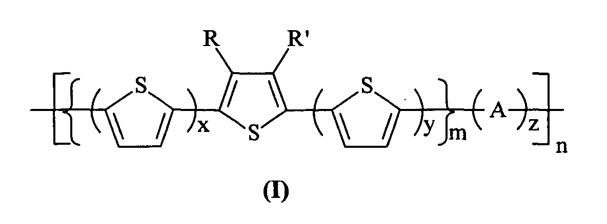
- aspects of the present invention include an electronic device containing a polythiophene of Formula (I) wherein R and R' are side chains; A is a divalent linkage; x and y represent the number of unsubstituted thienylene units; z is 0 or 1, and wherein the sum of x and y is greater than zero; m represents the number of segments; and n represents the degree of polymerization; an electronic device wherein R and R' are independently selected from alkyl and substituted alkyl, and A is an arylene; a device wherein R and R' contain from about 3 to about 20 carbon atoms; an electronic device wherein R and R' are independently selected from the group consisting of alkyl, alkyl derivatives of alkoxyalkyl; siloxy-substituted alkyl, perhaloalkyl of perfluoroalkyl and polyether; A is selected from the group consisting of arylene of phenylene, biphenylene, phenanthrenylene
- the number average molecular weight (M n ) of the polythiophenes can be, for example, from about 2,000 to about 100,000, and more specifically, from about 4,000 to about 50,000, and the weight average molecular weight (M w ) thereof can be from about 4,000 to about 500,000, and more specifically, from about 5,000 to about 100,000 both as measured by gel permeation chromatography using polystyrene standards.
- side chains R and R' include alkyl with, for example, from about 1 to about 25, and more specifically, from about 4 to about 12 carbon atoms, such as butyl, pentyl, hexyl, heptyl, octyl, nonyl, decyl, undecyl, dodecyl, isomeric forms thereof, and the like; alkoxyalkyl with from 1 to about 25 carbon atoms, such as for example methoxypropyl, methoxybutyl, methoxyhexyl, methoxyhexyl, methoxyheptyl, and the like, polyether chains, such as polyethylene oxide, perhaloalkyl, such as perfluoroalkyl of, for example, nonafluorohexyl, nonafluoroheptyl, pentadecafluorooctyl, tridecafluorononyl, and the like, and a polysiloxy chain, such as trialkyl
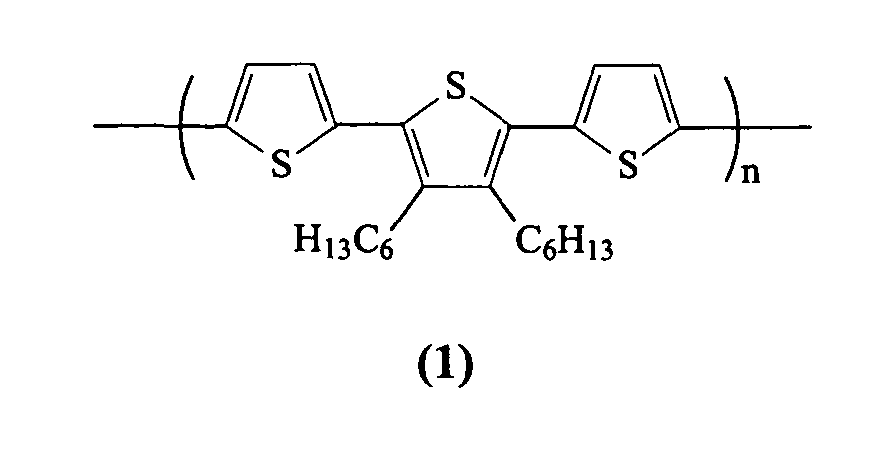
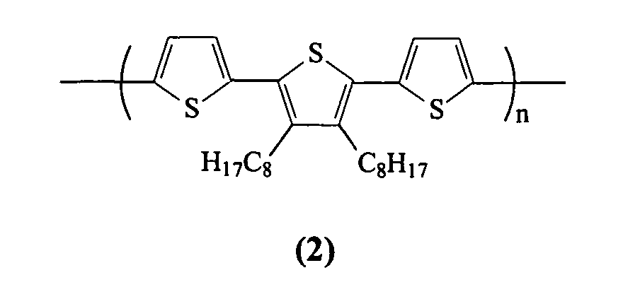
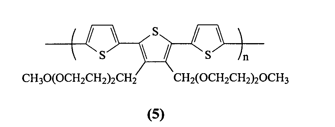
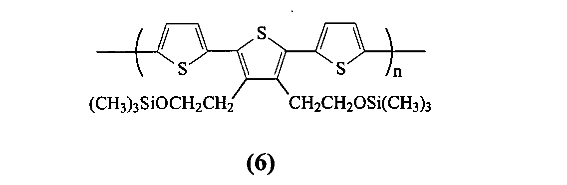
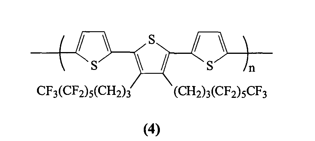
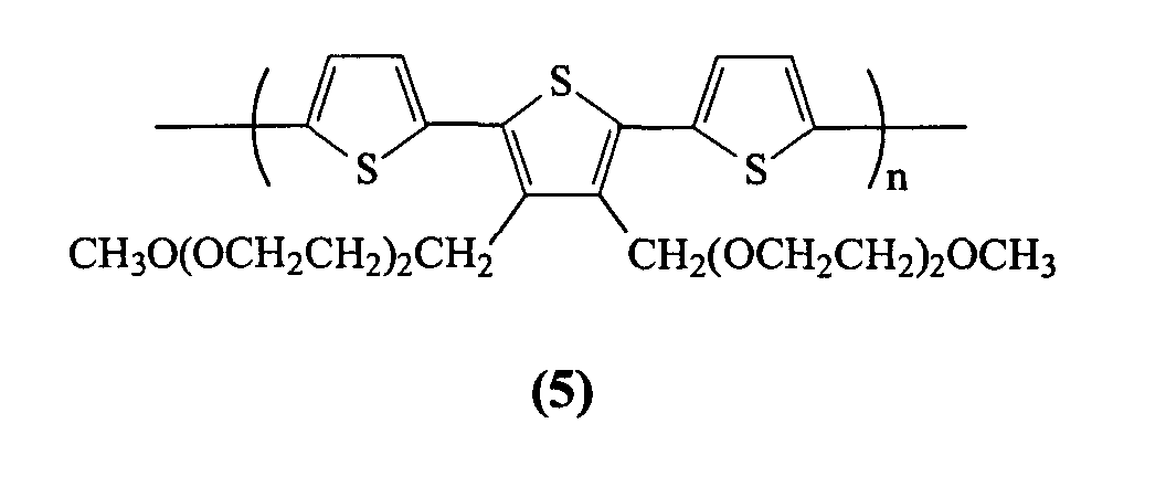
- examples of polythiophenes are: More specifically, examples of polythiophenes are:
- the polythiophenes, reference Formula (I), are comprised of regioregular segments of 3,4-disubstituted-2,5-thienylene units, unsubstituted 2,5-thienylene units, and an optional divalent linkage.
- the regioregularity of the side chains in polythiophene (I), reference Formulas (1) through (14), is believed to be capable of inducing molecular self-alignment during thin film fabrication under appropriate processing conditions enabling highly organized microstructures in thin films. Higher order microstructures in a semiconductor channel layer of a thin film transistor enhance transistor performance.
- the polythiophenes are stable in ambient conditions, and the devices fabricated from these polythiophenes are functionally more stable than regioregular polythiophenes such as regioregular poly(3-alkylthiophene-2,5-diyl).
- the devices fabricated from Formula (I) polythiophenes in embodiments thereof are generally stable for weeks or even months, such as for example about 3 weeks to about 12 weeks rather than days, such as for example about less than 5 days for the devices of regioregular poly(3-alkylthiophene-2,5-diyl) when exposed to ambient oxygen; also the devices fabricated from the polythiophenes provide higher current on/off ratios, and their performance does not change as rapidly as those of poly(3-alkylthiophene-2,5-diyl) when no rigorous procedural precautions are taken to exclude ambient oxygen during material preparation, device fabrication, and evaluation.
- the materials stability against oxidative doping is particularly useful for low-cost device manufacturing; since the materials are more stable, they usually do not have to be handled in a strictly inert atmosphere and the processes of preparation are, therefore, simpler and more cost effective, and which processes are amenable to simple large-scale production processes.
- the polythiophenes in embodiments are soluble in common coating solvents; for example, they possess a solubility of at least about 0.1 percent by weight, and more specifically, from about 0.5 percent to about 15 percent by weight in such solvents as methylene chloride, 1,2-dichloroethane, tetrahydrofuran, toluene, xylene, mesitylene, chlorobenzene, and the like.
- the polythiophenes when fabricated as semiconductor channel layers in thin film transistor devices provide a stable conductivity of, for example, from about 10 -9 S/cm to about 10 -6 S/cm, and more specifically, from about 10 -8 S/cm to about 10 -7 S/cm as determined by conventional four-probe conductivity measurement.
- the polythiophenes of the present invention can be prepared by polymerization of a properly constructed monomer, such as for example a trithiophene monomer, 2,5-bis(2-thienyl)-3,4-di-R-thiophene (IIa), or 2,5-bis(5-bromo-2-thienyl)-3,4-di-R-thiophene (IIb) for the preparation of illustrative polythiophenes (Ia) and (Ib) according to Scheme 1.
- a properly constructed monomer such as for example a trithiophene monomer, 2,5-bis(2-thienyl)-3,4-di-R-thiophene (IIa), or 2,5-bis(5-bromo-2-thienyl)-3,4-di-R-thiophene (IIb) for the preparation of illustrative polythiophenes (Ia) and (Ib) according to Scheme 1.
- polythiophenes (Ia) and (IIb) As the monomers ((IIa) and (IIb) carry two side chains on their respectively central thienylene units, their polymerizations, therefore, lead to polythiophenes (Ia) and (Ib) whose side chains are regioregularly positioned on their respective polythiophene backbones. Unlike the preparation of regioregular polythiophenes, such as poly(3-alkylthiophene-2,5-diyl) which require regioregular coupling reaction, the polythiophenes of the present invention can be prepared by general polymerization techniques without regioregularity complications.
- (Ia) can be prepared from monomer (IIa) by FeCl 3 -mediated oxidative coupling polymerization or from monomer (IIb) by treating with Reike zinc, followed by addition of Ni(dppe)Cl 2 catalyst.
- Polythiophene (IIb) can be readily obtained from (IIb) by Suzuki coupling reaction with appropriate arylene diboronate.
- the polymerization of (IIa) can be accomplished by adding a solution of 1 molar equivalent of (IIa) in a chlorinated solvent, such as chloroform, to a suspension of about 1 to about 5 molar equivalent of anhydrous FeCl 3 in chloroform under a blanket of dried air.
- a chlorinated solvent such as chloroform
- the resultant mixture is allowed to react at a temperature of about 25°C to about 50°C under a blanket of dried air or with a slow stream of dried air bubbling through the reaction mixture for a period of about 30 minutes to about 48 hours.
- the polymer product is isolated by washing the reaction mixture with water or dilute aqueous hydrochloric acid solution, stirring with dilute aqueous ammonium solution, followed by washing with water, and then precipitated from methanol or acetone.
- Reike zinc method 10 mmolar equivalents of (IIb) in anhydrous tetrahydrofuran is added dropwise over a period of 20 minutes to 40 minutes to a well-stirred suspension of 11 mmolar equivalent of freshly prepared Reike Zn in anhydrous tetrahydrofuran, and the resulting mixture is then permitted to react for about 30 minutes to about 2 hours at room temperature, about 22°C to about 25°C.
- polythiophene (Ib) can be obtained by the Suzuki coupling reaction of monomer (IIb) with an appropriate arylene-diboronate.
- FIG. 1 to 4 Illustrated in Figures 1 to 4 are various representative embodiments of the present invention and wherein the polythiophenes are selected as the channel materials in thin film transistor (TFT) configurations.
- TFT thin film transistor
- FIG. 1 there is schematically illustrated a thin film transistor configuration 10 comprised of a substrate 16, in contact therewith a metal contact 18 (gate electrode) and a layer of an insulating dielectric layer 14 contained thereon or on top of which two metal contacts, 20 and 22 (source and drain electrodes) are deposited. Over and between the metal contacts 20 and 22 is the polythiophene semiconductor layer 12.
- Figure 2 schematically illustrates another thin film transistor configuration 30 comprised of a substrate 36, a gate electrode 38, a source electrode 40, and a drain electrode 42, an insulating dielectric layer 34, and the polythiophene semiconductor layer 32.
- Figures 3 schematically illustrates a thin film transistor configuration 50 comprised of a heavily n-doped silicon wafer 56 which acts as a gate electrode, a thermally grown silicon oxide dielectric layer 54, and the polythiophene semiconductor layer 52, on top of which are deposited a source electrode 60 and a drain electrode 62.
- Figure 4 schematically illustrates an additional thin film transistor configuration 70 comprised of substrate 76, a gate electrode 78, a source electrode 80, a drain electrode 82, a polythiophene semiconductor layer 72, and an insulating dielectric layer 74.
- an optional protecting layer may be incorporated on top of each of the transistor configurations of Figures 1, 2, 3 and 4.
- the insulating dielectric layer 74 may also be able to function as a protecting layer.
- the substrate layer may generally be a silicon material inclusive of various appropriate forms of silicon, glass plate, plastic film or sheet, or the like depending on the intended applications.
- plastic substrate such as for example polyester, polycarbonate, polyimide sheets, and the like, may be preferred.
- the thickness of the substrate may be from about 10 micrometers to over 10 millimeters with a specific thickness being from about 50 to about 100 micrometers, especially for a flexible plastic substrate, and from about 1 to about 10 millimeters for a rigid substrate such as glass or silicon.
- the insulating dielectric layer which separates the gate electrode from the source and drain electrodes and in contact with the semiconductor layer, can generally be an inorganic material film, an organic polymer film, or an organic-inorganic composite film.
- the thickness of the dielectric layer is, for example, from about 10 nanometers to about 1 micrometer, with the more specific thickness being about 100 nanometers to about 500 nanometers.
- Illustrative examples of inorganic materials suitable as the dielectric layer include silicon oxide, silicon nitride, aluminum oxide, barium titanate, barium zirconate titanate, and the like; illustrative examples of organic polymers for the dielectric layer include polyesters, polycarbonates, poly(vinyl phenol), polyimides, polystyrene, poly(methacrylate)s, poly(acrylate)s, epoxy resin, and the like; while illustrative examples of inorganic-organic composite materials include nanosized metal oxide particles dispersed in polymers such as polyester, polyimide, epoxy resin and the like.
- the insulating dielectric layer is generally of a thickness of from about 50 nanometers to about 500 nanometers depending on the dielectric constant of the dielectric material used. More specifically, the dielectric material has a dielectric constant of at least about 3, so that a suitable dielectric thickness of about 300 nanometers would provide a desirable capacitance, for example, about of 10 -9 to about 10 -7 F/cm 2 .
- the active semiconductor layer comprised of the polythiophenes illustrated herein, and wherein the thickness of this layer is generally about 10 nanometers to about 1 micrometer with the thickness being about 40 to about 100 nanometers.
- This layer can generally be fabricated by solution processes such as spin coating, casting, screen, stamp, or jet printing of a solution of the polythiophenes of the present invention.
- the gate electrode can be a thin metal film, a conducting polymer film, a conducting film made from conducting ink or paste, or the substrate itself (for example heavily doped silicon).
- gate electrode materials include but are not restricted to aluminum, gold, chromium, indium tin oxide, conducting polymers, such as polystyrene sulfonate-doped poly(3,4-ethylenedioxythiophene) (PSS-/PEDOT), conducting ink/paste comprised of carbon black/graphite or colloidal silver dispersion in polymer binders, such as ELECTRODAG available from Acheson Colloids Company and silver filled electrically conductive thermoplastic ink available from Noelle Industries, and the like.
- conducting polymers such as polystyrene sulfonate-doped poly(3,4-ethylenedioxythiophene) (PSS-/PEDOT)
- conducting ink/paste comprised of carbon black/graphite or colloidal silver dispersion in polymer binders
- the gate layer can be prepared by vacuum evaporation, sputtering of metals or conductive metal oxides, coating from conducting polymer solutions or conducting inks by spin coating, casting or printing.
- the thickness of the gate electrode layer is in the range of about 10 nanometers to about 10 micrometers, and the preferred thickness is in the range of about 10 to about 200 nanometers for metal films and in the range of about 1 to about 10 micrometers for polymer conductors.
- the source and drain electrode layer can be fabricated from materials which provide a low-resistance ohmic contact to the semiconductor layer.
- Typical materials suitable for use as source and drain electrodes include those of the gate electrode materials such as gold, nickel, aluminum, platinum, conducting polymers, and conducting inks.
- Typical thickness of this layer is about, for example, from about 40 nanometers to about 1 micrometer with the more specific thickness being about 100 to about 400 nanometers.
- the TFT device structure consists of a semiconductor channel with a width W and length L.
- the semiconductor channel width may be from about 10 micrometers to about 5 millimeters, with the preferred channel width being about 100 micrometers to about 1 millimeter.
- the semiconductor channel length may be from about 1 micrometer to about 1 millimeter with the more specific channel length being from about 5 micrometers to about 100 micrometers.
- the source electrode is grounded and a bias voltage of generally about 0 volt to about -80 volts is applied to the drain electrode to collect the charge carriers transported across the semiconductor channel when a voltage of generally about +10 volts to about -80 volts is applied to the gate electrode.
- the bottom-contact test device was comprised of a series of photolithographically pre-patterned transistor's dielectric layers and electrodes with defined channel widths and lengths on a glass substrate.
- the gate electrode on the glass substrate was comprised of chromium of about 80 nanometers in thickness.
- the gate dielectric was a 300 nanometers thick silicon nitride having a capacitance of about 22 nF/cm 2 (nanofarads/square centimeter).
- the source and drain contacts comprised of gold of about 100 nanometers in thickness.
- test polythiophene semiconductor layer of about 30 nanometers to 100 nanometers in thickness was then deposited by spin coating under ambient conditions without taking any precautions to exclude it from exposure to ambient oxygen, moisture, or light.
- the solution used in fabricating the semiconductor layer was comprised of 1 percent by weight of the polythiophene in an appropriate solvent, and was filtered through a 0.45 ⁇ m filter before use.
- the spin coating was accomplished at a spinning speed of 1,000 rpm for about 35 seconds.
- the resulting coated device was dried in vacuo at 80°C for 20 hours, and was then ready for evaluation.
- the top-contact test device was comprised of an n-doped silicon wafer with a thermally grown silicon oxide layer of a thickness of about 110 nanometers thereon.
- the wafer functioned as the gate electrode while the silicon oxide layer acted as the gate dielectric and had a capacitance of about 32 nF/cm 2 .
- the silicon wafer was first cleaned with methanol, air dried, and then immersed in a 0.01 M solution of 1,1,1,3,3,3-hexamethyldisilazane in dichloromethane for 30 minutes at room temperature, 22°C to 25°C. Subsequently, the wafer was washed with dichloromethane and dried.
- the semiconductor polythiophene layer of about 30 nanometers to about 100 nanometers in thickness was then deposited on top of the silicon oxide dielectric layer by spin coating and dried in vacuo at 80°C for 20 hours. No precautions were taken to exclude the materials from exposure to ambient oxygen, moisture, or light during device fabrication. Subsequently, the gold source and drain electrodes were deposited on top of the semiconductor polythiophene layer by vacuum deposition through a shadow mask with various channel lengths and widths, thus creating a series of transistors of various dimensions. . For consistency, the devices after fabrication were kept in a dry atmosphere of about 30 percent relative humidity in the dark before and after evaluation.
- I SD C i ⁇ (W/2L) (V G -V T ) 2
- I SD the drain current at the saturated regime
- W and L are, respectively, the semiconductor channel width and length
- Ci is the capacitance per unit area of the gate dielectric layer
- V G and V T are, respectively, the gate voltage and threshold voltage.
- a property of value for the thin film transistor is its current on/off ratio, which is the ratio of the saturation source-drain current when the gate voltage V G is equal to or greater than the drain voltage V D to the source-drain current when the gate voltage V G is zero.
- This material was purchased from Aldrich Chemical and was purified by three successive precipitations of its solution in chlorobenzene from methanol.
- the semiconductor polythiophene layers were laid down on the devices in ambient conditions by spin coating a 1 percent by weight solution of regioregular poly(3-hexythiophene-2,5-diyl) in chlorobenzene according to the procedures as described herein before.
- the devices were dried in vacuo at 80°C for 20 hours before evaluation. The following summarizes the average properties from at least five transistors for each device:
- the observed low initial current on/off ratios are an indication of the propensity of poly(3-hexythiophene-2,5-diyl) towards oxidative doping, that is the instability of poly(3-hexythiophene-2,5-diyl) in the presence of ambient oxygen.
- the significant reductions in the current on/off ratios over just a five-day period further confirm the extreme functional instability of poly(3-hexythiophene-2,5-diyl) in ambient conditions.
- 3,4-Dioctylthiophene 2 M octylmagnesium bromide (100 milliliters, 0.2 mol) in anhydrous ethyl ether was added to a well-stirred mixture of dichloro[1,3-bis(diphenylphosphino)-propane]nickel(ll) (0.2 gram) and 3,4-dibromothiophene (20.16 grams, 0.0833 mol) in 200 milliliters of anhydrous ethyl ether in a 500 milliliter round bottom flask cooled with an ice bath under an inert atmosphere.
- the nickel complex reacted immediately with the Grignard reagent and the resulting reaction mixture was allowed to warm up to room temperature. An exothermic reaction started within 30 minutes and the ethyl ether began to reflux gently. After stirring for another 2 hours at room temperature, the reaction mixture was refluxed for 6 hours, then cooled in an ice bath, and hydrolyzed with aqueous 2N hydrochloric acid. The organic layer was separated and washed successively with water, brine, and again with water, dried over anhydrous sodium sulfate, and filtered. After evaporation of the solvent, the residue was distilled under reduced pressure through Kugelrohr apparatus to provide 21.3 grams of 3,4-dioctylthiophene as a colorless liquid.
- N-bromosuccinimide (4.6 grams, 25.7 mmol) was added to a well-stirred solution of 3,4-dioctylthiophene (3.6 grams, 11.7 mmol) in a mixture of 30 milliliters of dichloromethane and 10 milliliters of acetic acid in a 100 milliliter round-bottomed flask. The reaction was monitored by thin layer chromatography and was complete in about 35 minutes. The mixture was diluted with 160 milliliters of dichloromethane and filtered to remove succinimide.
- 2,5-Bis(2-thienyl)-3,4-dioctylthiophene In a dry box under an inert atmosphere, Pd(PPh 3 ) 2 Cl 2 (0.15 gram, 0.2 mmol) was added to a mixture of 2,5-dibromo-3,4-dioctylthiophene (4.2 grams, 9.0 mmol) and 2-(tributylstannyl)-thiophene (7.4 grams, 19.8 mmol) in anhydrous tetrahydrofuran (50 milliliters) in a 250 milliliter round-bottomed flask. The mixture was then refluxed for 12 hours and the solvent was removed by evaporation. The crude product thus obtained was purified by flash chromatography on silica gel using hexane as eluent to give 3.1 grams of 2,5-bis(2-thienyl)-3,4-dioctylthiophene.
- N-bromo succinimide (2.8 grams, 15.7 mmol) was added to a well-stirred solution of 2,5-bis(2-thienyl)-3,4-dioctylthiophene (3.6 grams, 7.6 mmol) of N,N-dimethylformamide (30 milliliters) in a 100 milliliter round-bottomed flask cooled with an ice-bath. After addition, the mixture was allowed to warm up to room temperature slowly. The reaction was monitored by thin layer chromotography and was stopped after 3 hours of reaction.
- test devices Two test devices, one bottom-contact and one top-contact in configuration as schematically represented in Figures 1 and 3, respectively, were fabricated using the above polythiophene in accordance with the fabrication procedures described above.
- the devices were dried in vacuo at 80°C for 20 hours before evaluation. The following summarizes the average properties from at least five transistors for each device
Landscapes
- Chemical & Material Sciences (AREA)
- Health & Medical Sciences (AREA)
- Chemical Kinetics & Catalysis (AREA)
- Medicinal Chemistry (AREA)
- Polymers & Plastics (AREA)
- Organic Chemistry (AREA)
- Engineering & Computer Science (AREA)
- Materials Engineering (AREA)
- Thin Film Transistor (AREA)
- Electroluminescent Light Sources (AREA)
- Polyoxymethylene Polymers And Polymers With Carbon-To-Carbon Bonds (AREA)
Abstract

Description
- The present invention is generally directed to organic microelectronic devices, and more specifically, in embodiments to the use of a class of polythiophenes as active materials in thin film transistors. The polythiophenes selected can be comprised of repeating thienylene units in which only certain thienylenes possess side chains, and which thienylene units are arranged in a regioregular manner on the polythiophene backbone.
- The polythiophenes are in embodiments substantially stable enabling their device fabrication to be accomplished at ambient conditions, and wherein the devices provide higher current on/off ratios, and are operationally more stable as their performance usually does not degrade as rapidly as those of known regioregular polythiophenes such as regioregular poly(3-alkylthiophene-2,5-diyl). More specifically, the polythiophenes of the present invention contain in embodiments repeating segments of 3,4-disubstituted-2,5-thienylene units flanked by unsubstituted 2,5-thienylene units and an optional divalent linkage. The side chains assist in inducing and facilitating molecular self-organization of the polythiophenes during film fabrication, while the unsubstituted thienylene units and the optional divalent linkage, which have some degree of rotational freedom, can disrupt the extended π-conjugation along the polythiophene chain, thus suppressing its propensity towards oxidative doping.
- Semiconductive polymers like certain polythiophenes, which are useful as active semiconductor materials in thin film transistors (TFTs), have been reported. A number of these polymers have reasonably good solubility in organic solvents and are thus able to be fabricated as semiconductor channel layers in TFTs by solution processes, such as spin coating, solution casting, dip coating, screen printing, stamp printing, jet printing, and the like. Their ability to be fabricated via common solution processes would render their manufacturing simpler and cost effective as compared to the costly conventional photolithographic processes typical of the silicon-based devices such as hydrogenated amorphous silicon TFTs. Moreover, desired are transistors fabricated with polymer materials, such as polythiophenes, referred to as polymer TFTs, include excellent mechanical durability and structural flexibility, which may be highly desirable for fabricating flexible TFTs on plastic substrates. Flexible TFTs would enable the design of electronic devices which usually require structural flexibility and mechanical durability characteristics. The use of plastic substrates, together with an organic or polymer transistor component, can transform the traditionally rigid silicon TFT into a mechanically more durable and structurally flexible polymer TFT design. The latter is of particular appeal to large-area devices, such as large-area image sensors, electronic paper and other display media as flexible TFTs, could enable a compact and structurally flexible design. Also, the selection of polymer TFTs for integrated circuit logic elements for low-end microelectronics, such as smart cards and radio frequency identification (RFID) tags, and memory/storage devices may also greatly enhance their mechanical durability, thus their useful life span. Nonetheless, many of the semiconductor polythiophenes are not stable when exposed to air as they become oxidatively doped by ambient oxygen resulting in increased conductivity. The result is larger off-current and thus lower current on/off ratio for the devices fabricated from these materials. Accordingly, with many of these materials, rigorous precautions have to be undertaken during materials processing and device fabrication to exclude environmental oxygen to avoid oxidative doping. These precautionary measures add to the cost of manufacturing, therefore, offsetting the appeal of certain polymer TFTs as an economical alternative to amorphous silicon technology, particularly for large-area devices. These and other disadvantages are avoided or minimized in embodiments of the present invention.
- Illustrated in Figures 1 to 4 are various representative embodiments of the present invention and wherein polythiophenes are selected as the channel materials in thin film transistor (TFT) configurations.
- It is a feature of the present invention to provide semiconductor polymers, such as polythiophenes, which are useful for microelectronic device applications like thin film transistor devices.
- It is another feature of the present invention to provide polythiophenes with a band gap of from about 1.5 eV to about 3 eV as determined from the absorption spectra of thin films thereof, and which polythiophenes are suitable for use as thin film transistor semiconductor channel layer materials.
- In yet a further feature of the present invention there are provided polythiophenes which are useful as microelectronic components, and which polythiophenes have reasonable solubility of, for example, at least about 0.1 percent by weight in common organic solvents, such as methylene chloride, tetrahydrofuran, toluene, xylene, mesitylene, chlorobenzene, and the like, and thus can be economically fabricated by solution processes, such as spin coating, screen printing, stamp printing, dip coating, solution casting, jet printing and the like.
- Another feature of the present invention resides in providing electronic devices, such as thin film transistors with a polythiophene channel layer, and which layer has a conductivity of from 10-6 to about 10-9 S/cm (Siemens/centimeter).
- Also, in yet another feature of the present invention there are provided polythiophenes and devices thereof, and which devices exhibit enhanced resistance to the adverse effects of oxygen, that is, these devices exhibit relatively high current on/off ratios, and their performance does not usually degrade as rapidly or minimal degradation results as those fabricated from regioregular polythiophenes such as regioregular poly(3-alkylthiophene-2,5-diyl).
- Additionally, in a further feature of the present invention there is provided a class of polythiophenes with unique structural features which are conducive to molecular self-alignment under appropriate processing conditions, and which structural features also enhance the stability of device performance. Proper molecular alignment can result in higher molecular structural order in thin films, permitting efficient charge carrier transport, and thus higher electrical performance.
- Aspects of the present invention include an electronic device containing a polythiophene of Formula (I)wherein R and R' are side chains; A is a divalent linkage; x and y represent the number of unsubstituted thienylene units; z is 0 or 1, and wherein the sum of x and y is greater than zero; m represents the number of segments; and n represents the degree of polymerization; an electronic device wherein R and R' are independently selected from alkyl and substituted alkyl, and A is an arylene; a device wherein R and R' contain from about 3 to about 20 carbon atoms; an electronic device wherein R and R' are independently selected from the group consisting of alkyl, alkyl derivatives of alkoxyalkyl; siloxy-substituted alkyl, perhaloalkyl of perfluoroalkyl and polyether; A is selected from the group consisting of arylene of phenylene, biphenylene, phenanthrenylene, dihydrophenanthrenylene, fluorenylene, oligoarylene, methylene, polymethylene, dialkylmethylene, dioxyalkylene, dioxyarylene, and oligoethylene oxide; a device wherein the R and R' are independently selected from the group consisting of propyl, butyl, pentyl, hexyl, heptyl, octyl, nonyl, decyl, undecyl, dodecyl, tridecyl, tetradecyl, pentadecyl, and isomers thereof; a device wherein A is arylene with from about 6 to about 40 carbon atoms; a device wherein R and R' are selected from the group consisting of hexyl, heptyl, octyl, nonyl, decyl, undecyl, dodecyl, tridecyl, tetradecyl, and pentadecyl; A is selected from the group consisting of phenylene, biphenylene, and fluorenylene; x and y are each independently a number of from zero to about 10; and m is a number of from 1 to about 5; an electronic device wherein n is from about 7 to about 5,000; the number average molecular weight (Mn) of the polythiophene is from about 2,000 to about 100,000; weight average molecular weight (Mw) is from about 4,000 to about 500,000, both as measured by gel permeation chromatography using polystyrene standards; a thin film transistor comprised of a substrate, a gate electrode, a gate dielectric layer, a source electrode and a drain electrode, and in contact with the source and drain electrodes and the gate dielectric layer, a semiconductor layer comprised of a polythiophene; a thin film transistor device wherein the R and R' are independently selected from the group consisting of alkyl, alkoxyalkyl, siloxy-substituted alkyl, and perhaloalkyl; A is selected from the group consisting of phenylene, biphenylene, phenanthrenylene, dihydrophenanthrenylene, fluorenylene, oligoarylene, methylene, polymethylene, dialkylmethylene, dioxyalkylene, dioxyarylene, and oligoethylene oxide; a thin film transistor device wherein n is from about 5 to about 5,000, the number average molecular weight (Mn) of the polythiophene is from about 4,000 to about 50,000, and the weight average molecular weight (Mw) is from about 5,000 to about 100,000 both as measured by gel permeation chromatography using polystyrene standards; a thin film transistor device wherein the R and R' are alkyls containing from about 3 to about 20 carbon atoms; a thin film transistor device wherein A is arylene with from about 6 to about 30 carbon atoms; a thin film transistor device wherein A is an arylene with from about 6 to about 24 carbon atoms; a thin film transistor device wherein A is phenylene, biphenylene, or fluorenylene; a thin film transistor device wherein a protective layer is present; a device wherein the polythiophene is selected from the group consisting of polythiophenes of Formulas (1) through (14)


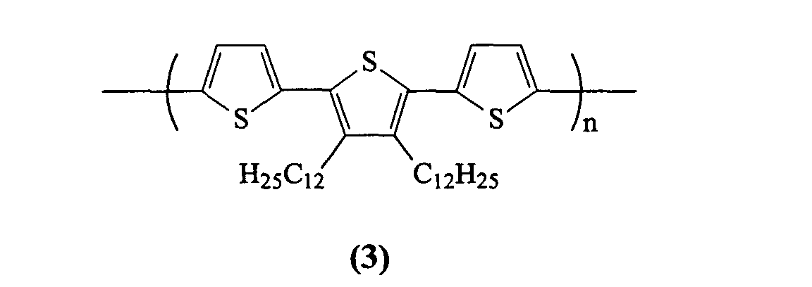

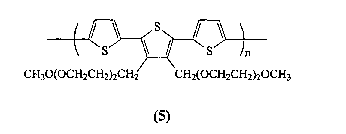
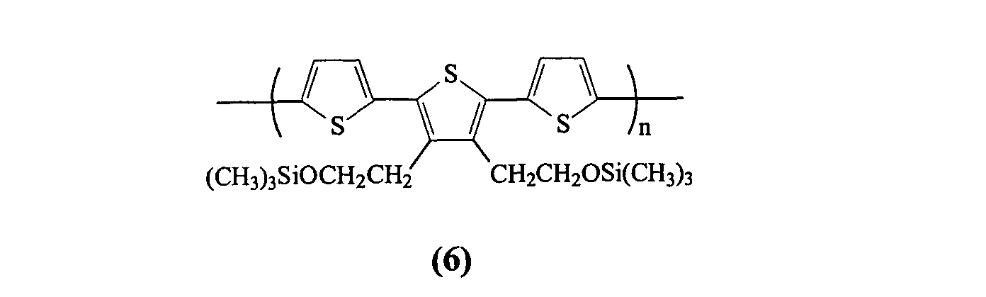
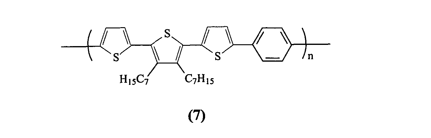
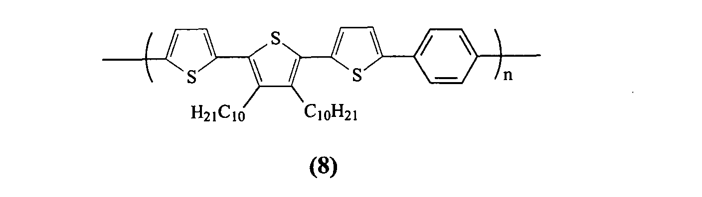


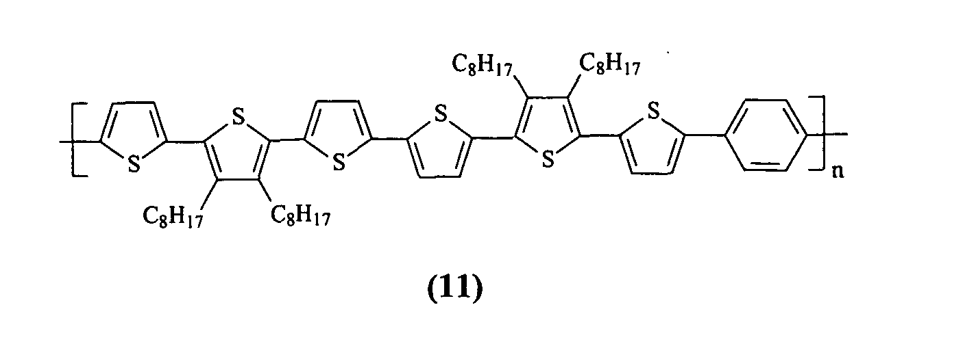

 a device wherein n is from about 5 to about 5,000; a device wherein n is from about 10 to about 1,000; a device wherein Mn is from about 4,000 to about 50,000, and Mw is from about 5,000 to about 100,000; a device wherein the polythiophene is selected from the group consisting of polythiophenes of Formulas (1) through (8)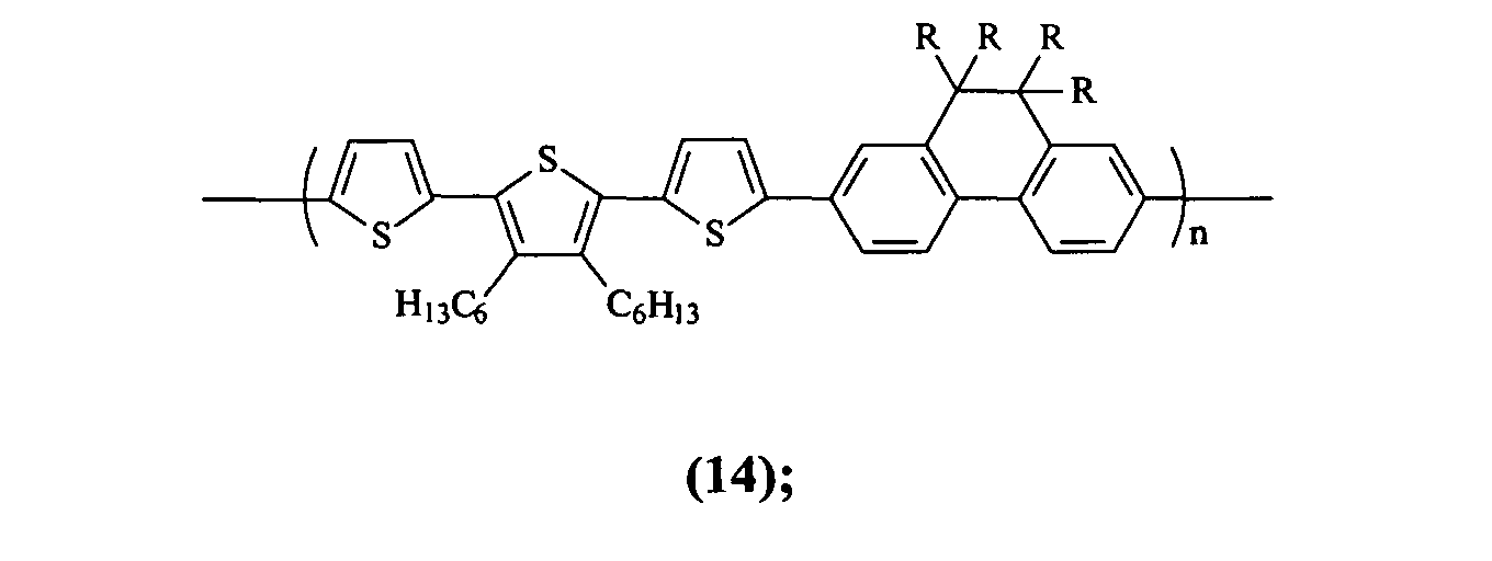


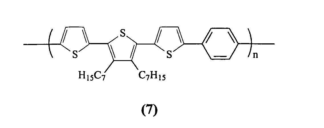 a thin film transistor device wherein the polythiophene is selected from the group consisting of polythiophenes of Formulas (1) through (14)

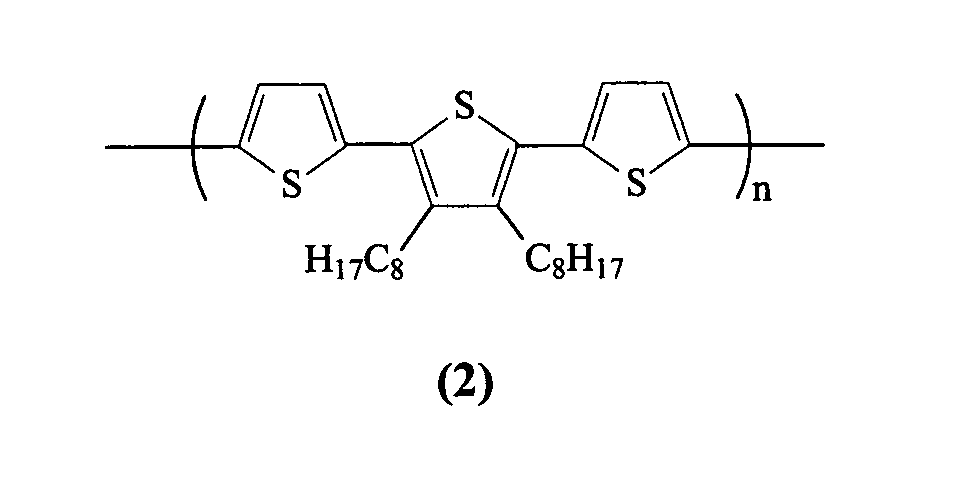


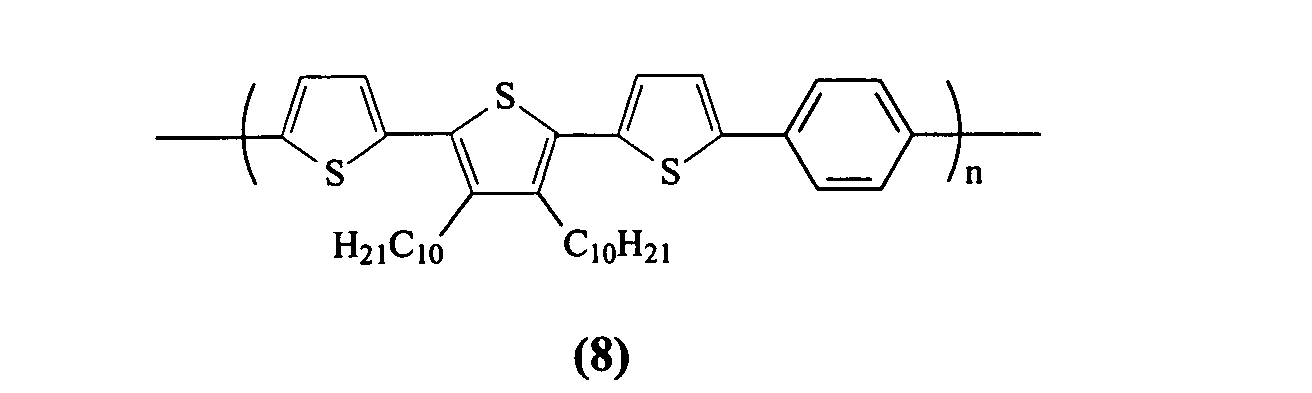


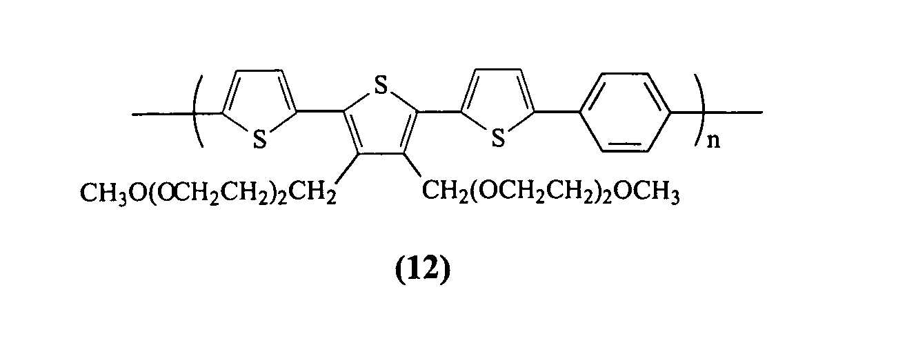
 a thin film transistor device wherein the polythiophene is selected from the group consisting of polythiophenes of Formulas (1) through (8)



 and optionally wherein n is from about 5 to about 5,000; a device wherein x, y and m are from 1 to 3; and z is 0 or 1, and which device is a thin film transistor; a device wherein x, y and m are 1; and z is 0 or 1, and which device is a thin film transistor; a device wherein x, y and m are from 1 to 3; and z is 0 or 1, and which device is a thin film transistor; a device wherein x, y and m are 1; and z is 0 or 1, or wherein x, y and m are 1; and z is 0, and which device is a thin film transistor; a thin film transistor device wherein the substrate is a plastic sheet of a polyester, a polycarbonate, or a polyimide; the gate, source, and drain electrodes are comprised of gold, nickel, aluminum, platinum, indium titanium oxide, or a conductive polymer; and the gate dielectric layer is comprised of silicon nitride, silicon oxide, or an insulating polymer; a thin film transistor device wherein the substrate is glass or a plastic sheet; the gate, source and drain electrodes are each comprised of gold; and the gate dielectric layer is comprised of the organic polymer poly(methacrylate), poly(vinyl phenol); a thin film transistor device wherein the gate, source and drain electrodes are fabricated from a doped organic conductive polymer of polystyrene sulfonate-doped poly(3,4-ethylenedioxythiophene) or a conductive ink/paste comprised of a colloidal dispersion of silver in a polymer binder, and the gate dielectric layer is organic polymer or an inorganic oxide particle-polymer composite; and polythiophenes encompassed by
 wherein R and R' are side chains independently selected, for example, from the group consisting of alkyl, alkyl derivatives, such as alkoxyalkyl; siloxy-substituted alkyl, perhaloalkyl, such as perfluoroalkyl, polyether, such as oligoethylene oxide, polysiloxy, and the like; A is a divalent linkage selected, for example, from the group consisting of arylene, such as phenylene, biphenylene, phenanthrenylene, dihydrophenanthrenylene, fluorenylene, oligoarylene, methylene, polymethylene, dialkylmethylene, dioxyalkylene, dioxyarylene, oligoethylene oxide, and the like; x and y are integers independently selected from 0 to 10, z is either 0 or 1 with the provision that the sum of x and y is greater zero; m is an integer of from 1 to about 5; and n is the degree of polymerization, and can generally be from about 5 to over 5,000, and more specifically, from about 10 to about 1,000. The number average molecular weight (Mn) of the polythiophenes can be, for example, from about 2,000 to about 100,000, and more specifically, from about 4,000 to about 50,000, and the weight average molecular weight (Mw) thereof can be from about 4,000 to about 500,000, and more specifically, from about 5,000 to about 100,000 both as measured by gel permeation chromatography using polystyrene standards.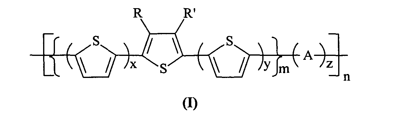
- Examples of the side chains R and R' include alkyl with, for example, from about 1 to about 25, and more specifically, from about 4 to about 12 carbon atoms, such as butyl, pentyl, hexyl, heptyl, octyl, nonyl, decyl, undecyl, dodecyl, isomeric forms thereof, and the like; alkoxyalkyl with from 1 to about 25 carbon atoms, such as for example methoxypropyl, methoxybutyl, methoxyhexyl, methoxyhexyl, methoxyheptyl, and the like, polyether chains, such as polyethylene oxide, perhaloalkyl, such as perfluoroalkyl of, for example, nonafluorohexyl, nonafluoroheptyl, pentadecafluorooctyl, tridecafluorononyl, and the like, and a polysiloxy chain, such as trialkylsiloxyalkyl, and the like.
- More specifically, examples of polythiophenes are

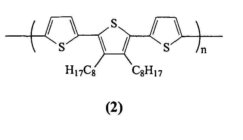


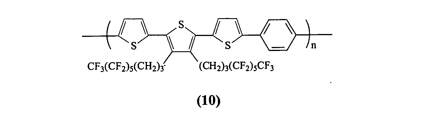


- The polythiophenes, reference Formula (I), are comprised of regioregular segments of 3,4-disubstituted-2,5-thienylene units, unsubstituted 2,5-thienylene units, and an optional divalent linkage. The regioregularity of the side chains in polythiophene (I), reference Formulas (1) through (14), is believed to be capable of inducing molecular self-alignment during thin film fabrication under appropriate processing conditions enabling highly organized microstructures in thin films. Higher order microstructures in a semiconductor channel layer of a thin film transistor enhance transistor performance. It is believed that these polythiophenes, when fabricated as thin films of about 10 nanometers to about 500 nanometers from their solutions in appropriate solvent systems, form strong intermolecular π-π stacks which are conducive to efficient charge carrier transport. The unsubstituted thienylene moieties in (I), by virtue of possessing some degree of rotational freedom, help to disrupt the extended intramolecular π-conjugation of (I) to an extent that is sufficient to suppress its propensity towards oxidative doping. Accordingly, the polythiophenes are stable in ambient conditions, and the devices fabricated from these polythiophenes are functionally more stable than regioregular polythiophenes such as regioregular poly(3-alkylthiophene-2,5-diyl). When unprotected, the devices fabricated from Formula (I) polythiophenes in embodiments thereof are generally stable for weeks or even months, such as for example about 3 weeks to about 12 weeks rather than days, such as for example about less than 5 days for the devices of regioregular poly(3-alkylthiophene-2,5-diyl) when exposed to ambient oxygen; also the devices fabricated from the polythiophenes provide higher current on/off ratios, and their performance does not change as rapidly as those of poly(3-alkylthiophene-2,5-diyl) when no rigorous procedural precautions are taken to exclude ambient oxygen during material preparation, device fabrication, and evaluation. The materials stability against oxidative doping is particularly useful for low-cost device manufacturing; since the materials are more stable, they usually do not have to be handled in a strictly inert atmosphere and the processes of preparation are, therefore, simpler and more cost effective, and which processes are amenable to simple large-scale production processes.
- The polythiophenes in embodiments are soluble in common coating solvents; for example, they possess a solubility of at least about 0.1 percent by weight, and more specifically, from about 0.5 percent to about 15 percent by weight in such solvents as methylene chloride, 1,2-dichloroethane, tetrahydrofuran, toluene, xylene, mesitylene, chlorobenzene, and the like. Moreover, the polythiophenes when fabricated as semiconductor channel layers in thin film transistor devices provide a stable conductivity of, for example, from about 10-9 S/cm to about 10-6 S/cm, and more specifically, from about 10-8 S/cm to about 10-7 S/cm as determined by conventional four-probe conductivity measurement.
- The polythiophenes of the present invention can be prepared by polymerization of a properly constructed monomer, such as for example a trithiophene monomer, 2,5-bis(2-thienyl)-3,4-di-R-thiophene (IIa), or 2,5-bis(5-bromo-2-thienyl)-3,4-di-R-thiophene (IIb) for the preparation of illustrative polythiophenes (Ia) and (Ib) according to Scheme 1. As the monomers ((IIa) and (IIb) carry two side chains on their respectively central thienylene units, their polymerizations, therefore, lead to polythiophenes (Ia) and (Ib) whose side chains are regioregularly positioned on their respective polythiophene backbones. Unlike the preparation of regioregular polythiophenes, such as poly(3-alkylthiophene-2,5-diyl) which require regioregular coupling reaction, the polythiophenes of the present invention can be prepared by general polymerization techniques without regioregularity complications. Specifically, (Ia) can be prepared from monomer (IIa) by FeCl3-mediated oxidative coupling polymerization or from monomer (IIb) by treating with Reike zinc, followed by addition of Ni(dppe)Cl2 catalyst. Polythiophene (IIb), on the other hand, can be readily obtained from (IIb) by Suzuki coupling reaction with appropriate arylene diboronate.

- Specifically, the polymerization of (IIa) can be accomplished by adding a solution of 1 molar equivalent of (IIa) in a chlorinated solvent, such as chloroform, to a suspension of about 1 to about 5 molar equivalent of anhydrous FeCl3 in chloroform under a blanket of dried air. The resultant mixture is allowed to react at a temperature of about 25°C to about 50°C under a blanket of dried air or with a slow stream of dried air bubbling through the reaction mixture for a period of about 30 minutes to about 48 hours. After the reaction, the polymer product is isolated by washing the reaction mixture with water or dilute aqueous hydrochloric acid solution, stirring with dilute aqueous ammonium solution, followed by washing with water, and then precipitated from methanol or acetone. For the Reike zinc method, 10 mmolar equivalents of (IIb) in anhydrous tetrahydrofuran is added dropwise over a period of 20 minutes to 40 minutes to a well-stirred suspension of 11 mmolar equivalent of freshly prepared Reike Zn in anhydrous tetrahydrofuran, and the resulting mixture is then permitted to react for about 30 minutes to about 2 hours at room temperature, about 22°C to about 25°C. Subsequently, a suspension of about 0.1 mmolar equivalent of Ni(dppe)Cl2 in anhydrous tetrahydrofuran is slowly added over a period of about 10 minutes to about 20 minutes, and the mixture is then heated at about 40°C to about 65°C for 2 to 5 hours. The reaction mixture is then poured into dilute hydrochloric acid solution in methanol with vigorous stirring to precipitate the polymer product. The latter is redissolved in hot tetrahydrofuran and then reprecipitated from dilute ammonia solution in methanol.
- More specifically, polythiophene (Ib) can be obtained by the Suzuki coupling reaction of monomer (IIb) with an appropriate arylene-diboronate. A mixture of equal molar equivalents of (IIa) and arylene-diboronate in toluene, about 2 to 6 molar percent of tetrakis(triphenylphosphine)-palladum, about 2 to about 4 molar equivalents of an inorganic base, such as sodium carbonate, in the form of a 1 M to 2 M aqueous solution, and about 1 to 5 mole percent of a phase transfer catalyst, such as tetrabutylamomonium chloride or tricaprylylmethylammonium chloride, is heated at about 90°C under an inert atmosphere for 48 hours. After polymerization, polythiophene product (Ib) is isolated by repeated precipitation from methonol.
- Illustrated in Figures 1 to 4 are various representative embodiments of the present invention and wherein the polythiophenes are selected as the channel materials in thin film transistor (TFT) configurations.
- In Figure 1 there is schematically illustrated a thin
film transistor configuration 10 comprised of asubstrate 16, in contact therewith a metal contact 18 (gate electrode) and a layer of an insulatingdielectric layer 14 contained thereon or on top of which two metal contacts, 20 and 22 (source and drain electrodes) are deposited. Over and between themetal contacts polythiophene semiconductor layer 12. - Figure 2 schematically illustrates another thin
film transistor configuration 30 comprised of asubstrate 36, agate electrode 38, asource electrode 40, and adrain electrode 42, an insulatingdielectric layer 34, and thepolythiophene semiconductor layer 32. - Figures 3 schematically illustrates a thin
film transistor configuration 50 comprised of a heavily n-dopedsilicon wafer 56 which acts as a gate electrode, a thermally grown silicon oxidedielectric layer 54, and thepolythiophene semiconductor layer 52, on top of which are deposited asource electrode 60 and adrain electrode 62. - Figure 4 schematically illustrates an additional thin
film transistor configuration 70 comprised ofsubstrate 76, agate electrode 78, asource electrode 80, adrain electrode 82, apolythiophene semiconductor layer 72, and an insulatingdielectric layer 74. - In some embodiments of the present invention, an optional protecting layer may be incorporated on top of each of the transistor configurations of Figures 1, 2, 3 and 4. For the thin film transistor configuration of Figure 4, the insulating
dielectric layer 74 may also be able to function as a protecting layer. - The substrate layer may generally be a silicon material inclusive of various appropriate forms of silicon, glass plate, plastic film or sheet, or the like depending on the intended applications. For structurally flexible devices, plastic substrate, such as for example polyester, polycarbonate, polyimide sheets, and the like, may be preferred. The thickness of the substrate may be from about 10 micrometers to over 10 millimeters with a specific thickness being from about 50 to about 100 micrometers, especially for a flexible plastic substrate, and from about 1 to about 10 millimeters for a rigid substrate such as glass or silicon.
- The insulating dielectric layer, which separates the gate electrode from the source and drain electrodes and in contact with the semiconductor layer, can generally be an inorganic material film, an organic polymer film, or an organic-inorganic composite film. The thickness of the dielectric layer is, for example, from about 10 nanometers to about 1 micrometer, with the more specific thickness being about 100 nanometers to about 500 nanometers. Illustrative examples of inorganic materials suitable as the dielectric layer include silicon oxide, silicon nitride, aluminum oxide, barium titanate, barium zirconate titanate, and the like; illustrative examples of organic polymers for the dielectric layer include polyesters, polycarbonates, poly(vinyl phenol), polyimides, polystyrene, poly(methacrylate)s, poly(acrylate)s, epoxy resin, and the like; while illustrative examples of inorganic-organic composite materials include nanosized metal oxide particles dispersed in polymers such as polyester, polyimide, epoxy resin and the like. The insulating dielectric layer is generally of a thickness of from about 50 nanometers to about 500 nanometers depending on the dielectric constant of the dielectric material used. More specifically, the dielectric material has a dielectric constant of at least about 3, so that a suitable dielectric thickness of about 300 nanometers would provide a desirable capacitance, for example, about of 10-9 to about 10-7 F/cm2.
- Situated between and in contact with the dielectric layer and the source/drain electrodes is the active semiconductor layer comprised of the polythiophenes illustrated herein, and wherein the thickness of this layer is generally about 10 nanometers to about 1 micrometer with the thickness being about 40 to about 100 nanometers. This layer can generally be fabricated by solution processes such as spin coating, casting, screen, stamp, or jet printing of a solution of the polythiophenes of the present invention.
- The gate electrode can be a thin metal film, a conducting polymer film, a conducting film made from conducting ink or paste, or the substrate itself (for example heavily doped silicon). Examples of gate electrode materials include but are not restricted to aluminum, gold, chromium, indium tin oxide, conducting polymers, such as polystyrene sulfonate-doped poly(3,4-ethylenedioxythiophene) (PSS-/PEDOT), conducting ink/paste comprised of carbon black/graphite or colloidal silver dispersion in polymer binders, such as ELECTRODAG available from Acheson Colloids Company and silver filled electrically conductive thermoplastic ink available from Noelle Industries, and the like. The gate layer can be prepared by vacuum evaporation, sputtering of metals or conductive metal oxides, coating from conducting polymer solutions or conducting inks by spin coating, casting or printing. The thickness of the gate electrode layer is in the range of about 10 nanometers to about 10 micrometers, and the preferred thickness is in the range of about 10 to about 200 nanometers for metal films and in the range of about 1 to about 10 micrometers for polymer conductors.
- The source and drain electrode layer can be fabricated from materials which provide a low-resistance ohmic contact to the semiconductor layer. Typical materials suitable for use as source and drain electrodes include those of the gate electrode materials such as gold, nickel, aluminum, platinum, conducting polymers, and conducting inks. Typical thickness of this layer is about, for example, from about 40 nanometers to about 1 micrometer with the more specific thickness being about 100 to about 400 nanometers. The TFT device structure consists of a semiconductor channel with a width W and length L. The semiconductor channel width may be from about 10 micrometers to about 5 millimeters, with the preferred channel width being about 100 micrometers to about 1 millimeter. The semiconductor channel length may be from about 1 micrometer to about 1 millimeter with the more specific channel length being from about 5 micrometers to about 100 micrometers.
- The source electrode is grounded and a bias voltage of generally about 0 volt to about -80 volts is applied to the drain electrode to collect the charge carriers transported across the semiconductor channel when a voltage of generally about +10 volts to about -80 volts is applied to the gate electrode.
- The following Examples are provided.
- There were selected a bottom-contact and a top-contact thin film transistor structures as schematically described by Figure 1 and Figure 3, respectively, as the primary test device configurations. The bottom-contact test device was comprised of a series of photolithographically pre-patterned transistor's dielectric layers and electrodes with defined channel widths and lengths on a glass substrate. The gate electrode on the glass substrate was comprised of chromium of about 80 nanometers in thickness. The gate dielectric was a 300 nanometers thick silicon nitride having a capacitance of about 22 nF/cm2 (nanofarads/square centimeter). On top of or coated on the gate dielectric layer there was provided by vacuum deposition the source and drain contacts comprised of gold of about 100 nanometers in thickness. The test polythiophene semiconductor layer of about 30 nanometers to 100 nanometers in thickness was then deposited by spin coating under ambient conditions without taking any precautions to exclude it from exposure to ambient oxygen, moisture, or light. The solution used in fabricating the semiconductor layer was comprised of 1 percent by weight of the polythiophene in an appropriate solvent, and was filtered through a 0.45 µm filter before use. The spin coating was accomplished at a spinning speed of 1,000 rpm for about 35 seconds. The resulting coated device was dried in vacuo at 80°C for 20 hours, and was then ready for evaluation.
- The top-contact test device was comprised of an n-doped silicon wafer with a thermally grown silicon oxide layer of a thickness of about 110 nanometers thereon. The wafer functioned as the gate electrode while the silicon oxide layer acted as the gate dielectric and had a capacitance of about 32 nF/cm2. The silicon wafer was first cleaned with methanol, air dried, and then immersed in a 0.01 M solution of 1,1,1,3,3,3-hexamethyldisilazane in dichloromethane for 30 minutes at room temperature, 22°C to 25°C. Subsequently, the wafer was washed with dichloromethane and dried. The semiconductor polythiophene layer of about 30 nanometers to about 100 nanometers in thickness was then deposited on top of the silicon oxide dielectric layer by spin coating and dried in vacuo at 80°C for 20 hours. No precautions were taken to exclude the materials from exposure to ambient oxygen, moisture, or light during device fabrication. Subsequently, the gold source and drain electrodes were deposited on top of the semiconductor polythiophene layer by vacuum deposition through a shadow mask with various channel lengths and widths, thus creating a series of transistors of various dimensions. . For consistency, the devices after fabrication were kept in a dry atmosphere of about 30 percent relative humidity in the dark before and after evaluation.
- The evaluation of field-effect transistor performance was accomplished in a black box at ambient conditions using a Keithley 4200 SCS semiconductor characterization system. The carrier mobility, µ, was calculated from the data in the saturated regime (gate voltage, VG < source-drain voltage, VSD) accordingly to equation (1)
- A property of value for the thin film transistor is its current on/off ratio, which is the ratio of the saturation source-drain current when the gate voltage VG is equal to or greater than the drain voltage VD to the source-drain current when the gate voltage VG is zero.
- A bottom-contact device and a top-contact device with configurations as described by Figures 1 and 3, respectively, were fabricated by essentially repeating the above except that the known regioregular polythiophene, poly(3-hexythiophene-2,5-diyl) was selected. This material was purchased from Aldrich Chemical and was purified by three successive precipitations of its solution in chlorobenzene from methanol.
- The semiconductor polythiophene layers were laid down on the devices in ambient conditions by spin coating a 1 percent by weight solution of regioregular poly(3-hexythiophene-2,5-diyl) in chlorobenzene according to the procedures as described herein before. The devices were dried in vacuo at 80°C for 20 hours before evaluation. The following summarizes the average properties from at least five transistors for each device:
- (1) Bottom-contact device (W = 1,000 µm; L = 10 µm)
Mobility: 1 to 2.3 x 10⁻³ cm2/V.sec
Initial current on-off ratio: 0.8 to 1 x 10³
Current on/off ratio after 5 days: 5 to 10 - (2) Top-contact device (W = 5,000 µm; L = 60 µm)
Mobility: 1 to 1.2 x 10⁻² cm2/V.sec
Initial on-off ratio: 1.5 to 2.1 x 10³
On-off ratio after 5 days: 5 to 10 -
- The observed low initial current on/off ratios are an indication of the propensity of poly(3-hexythiophene-2,5-diyl) towards oxidative doping, that is the instability of poly(3-hexythiophene-2,5-diyl) in the presence of ambient oxygen. The significant reductions in the current on/off ratios over just a five-day period further confirm the extreme functional instability of poly(3-hexythiophene-2,5-diyl) in ambient conditions.
- i) Monomer Synthesis: The monomer 2,5-bis(5-bromo-2-thienyl)-3,4-dioctylthiophene for the preparation of polythiophene (2) was synthesized as follows:
- 3,4-Dioctylthiophene: 2 M octylmagnesium bromide (100 milliliters, 0.2 mol) in anhydrous ethyl ether was added to a well-stirred mixture of dichloro[1,3-bis(diphenylphosphino)-propane]nickel(ll) (0.2 gram) and 3,4-dibromothiophene (20.16 grams, 0.0833 mol) in 200 milliliters of anhydrous ethyl ether in a 500 milliliter round bottom flask cooled with an ice bath under an inert atmosphere. The nickel complex reacted immediately with the Grignard reagent and the resulting reaction mixture was allowed to warm up to room temperature. An exothermic reaction started within 30 minutes and the ethyl ether began to reflux gently. After stirring for another 2 hours at room temperature, the reaction mixture was refluxed for 6 hours, then cooled in an ice bath, and hydrolyzed with aqueous 2N hydrochloric acid. The organic layer was separated and washed successively with water, brine, and again with water, dried over anhydrous sodium sulfate, and filtered. After evaporation of the solvent, the residue was distilled under reduced pressure through Kugelrohr apparatus to provide 21.3 grams of 3,4-dioctylthiophene as a colorless liquid.
- 1H NMR(CDCl3):
- δ 6.89 (s, 2H), 2.50 (t, J = 7.0 Hz, 4H), 1.64-1.58 (m, 4H), 1.40-1.28 (m, 20H), 0.89 (t, J = 6.5 Hz, 6H); 13C NMR (CDCl3) δ 142.1, 119.8, 31.9, 29.6 (2C), 29.5, 29.3, 28.8, 22.7, 14.1.
- 2,5-Dibromo-3,4-dioctylthiophene: N-bromosuccinimide (4.6 grams, 25.7 mmol) was added to a well-stirred solution of 3,4-dioctylthiophene (3.6 grams, 11.7 mmol) in a mixture of 30 milliliters of dichloromethane and 10 milliliters of acetic acid in a 100 milliliter round-bottomed flask. The reaction was monitored by thin layer chromatography and was complete in about 35 minutes. The mixture was diluted with 160 milliliters of dichloromethane and filtered to remove succinimide. The filtrate was washed with aqueous 2N sodium hydroxide solution, and then twice with water (2 X 100 milliliters). After drying with anhydrous sodium sulfate and removal of the solvent, 5.4 grams of 2,5-dibromo-3,4-dioctylthiophene as a light yellow liquid.
- 1H NMR (CDCl3):
- δ 2.50 (t, J = 7.0 Hz, 4H), 1.52-1.28 (m, 24H), 0.89 (t, J = 6.5 Hz, 6H).
- 2,5-Bis(2-thienyl)-3,4-dioctylthiophene: In a dry box under an inert atmosphere, Pd(PPh3)2Cl2 (0.15 gram, 0.2 mmol) was added to a mixture of 2,5-dibromo-3,4-dioctylthiophene (4.2 grams, 9.0 mmol) and 2-(tributylstannyl)-thiophene (7.4 grams, 19.8 mmol) in anhydrous tetrahydrofuran (50 milliliters) in a 250 milliliter round-bottomed flask. The mixture was then refluxed for 12 hours and the solvent was removed by evaporation. The crude product thus obtained was purified by flash chromatography on silica gel using hexane as eluent to give 3.1 grams of 2,5-bis(2-thienyl)-3,4-dioctylthiophene.
- 1H NMR (CDCl3):
- δ 7.31 (dd, J = 3.2, 0.5 Hz, 2H), 7.13 (dd, J = 2.2, 0.5 Hz, 2H), 7.06 (dd, J = 2.2, 4.5 Hz, 2H), 2.68 (dd, J = 7.6, 7.6 Hz, 4H), 1.59-1.53 (m, 4H), 1.42-1.27 (m, 20H), 0.91 (t, J = 6.5 Hz, 6H).
- 2,5-Bis(5-bromo-2-thienyl)-3,4-dioctylthiophene: N-bromo succinimide (2.8 grams, 15.7 mmol) was added to a well-stirred solution of 2,5-bis(2-thienyl)-3,4-dioctylthiophene (3.6 grams, 7.6 mmol) of N,N-dimethylformamide (30 milliliters) in a 100 milliliter round-bottomed flask cooled with an ice-bath. After addition, the mixture was allowed to warm up to room temperature slowly. The reaction was monitored by thin layer chromotography and was stopped after 3 hours of reaction. The resulting mixture was diluted with hexanes (170 milliliters) and washed with three times with 100 milliliters of water. The organic layer was separated, dried with anhydrous sodium sulfate, and vacuum evaporated to provide the crude product, which was purified by flash chromatography on silica gel using hexane as eluent to give 2.5 grams of 2,5-bis(5-bromo-2-thienyl)-3,4-dioctylthiophene.
- 1H NMR (CDCl3):
- δ 7.06 (d, J = 3.5 Hz, 2H), 6.86 (d, J = 3.5 Hz, 2H), 2.62 (dd, J = 7.3, 7.3 Hz, 4H), 1.55-1.49 (m, 4H), 1.41-1.28 (m, 20H), 0.89 (t, J = 6.5 Hz, 6H); 13C NMR (CDCl3) δ 140.6, 137.4, 130.2, 129.3, 126.2, 112.0, 31.9, 30.8, 29.8, 29.2 (2C), 28.1, 22.7, 14.2.
- Poly[2,5-bis(2-thienyl)-3,4-dioctylthiophene] (2): A well stirred suspension of freshly prepared Reike Zn (0.28 gram, 4.29 mmol) in anhydrous tetrahydrofuran (20 milliliters) under an inert atmosphere was added dropwise to a solution of 2,5-bis(5-bromo-2-thienyl)-3,4-dioctylthiophene (2.46 grams, 3.9 mmol) in anhydrous tetrahydrofuran (10 milliliters), and the mixture was permitted to react for 45 minutes at room temperature. Subsequently, a suspension of Ni(dppe)Cl2 (0.021 gram, 0.04 mmol) in anhydrous tetrahydrofuran (35 milliliters) was carefully added. The reaction mixture was heated at 60°C for 3 hours and then poured into 2N hydrochloric acid solution in methanol. The precipitated polythiophene product was filtered, redissolved in 70 milliliters of hot tetrahydrofuran, and precipitated from 2N ammonia solution in methanol. This procedure was repeated twice to remove the acid and oligomers. After drying in vacuo at room temperature, 1.6 grams of poly[2,5-bis(2-thienyl)-3,4-dioctylthiophene] (2), Mw, 41,900, Mn, 11,800 K, Tm, 180°C resulted.
- 1H NMR(CDCl3):
- δ 7.30, 7.13, 7.05, 2.73, 1.59, 1.45, 1.29, 0.89; 13C NMR (CDCl3) δ 140.4, 136.7, 135.1, 129.8, 126.4, 123.9, 31.9, 30.7, 29.9, 29.3, 28.3, 22.7, 14.2.
- Two test devices, one bottom-contact and one top-contact in configuration as schematically represented in Figures 1 and 3, respectively, were fabricated using the above polythiophene in accordance with the fabrication procedures described above. The devices were dried in vacuo at 80°C for 20 hours before evaluation. The following summarizes the average properties from at least five transistors for each device
- (1) Bottom-contact device (W = 1,000 µm; L = 10 µm)
Mobility: 3.4 x 10⁻⁴ to 1.3 x 10⁻³ cm2/V.sec
Initial current on/off ratio: 0.8 to 1.3 x 10⁴
Current on/off ratio after 5 days: 5.0 to 7.0 x 10³ - (2) Top-contact device (W = 5,000 µm; L = 60 µm)
Mobility: 1.3 to 3.1 x 10⁻³ cm2/V.sec
Initial on-off ratio: 1.5 to 2.6 x 10⁵
On-off ratio after 5 days: 1.1 - 2.0x 10⁵
On-off ratio after 30 days: 8.0 - 9.5x 10⁴ -
- The stability of the polythiophene semiconductor layer in embodiments of the present invention was demonstrated by the large initial current on/off rations and the slow reductions in current on/off ratio over time.
Claims (10)
- An electronic device containing a polythiophene of Formula (I)wherein R and R' are side chains; A is a divalent linkage; x and y represent the number of unsubstituted thienylene units or segments; z is 0 or 1, and wherein the sum of x and y is greater than zero; m represents the number of segments; and n represents the degree of polymerization.
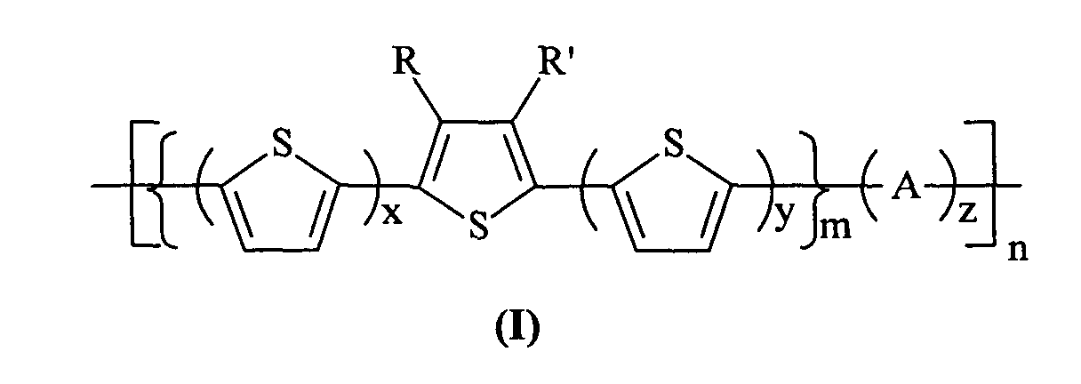
- An electronic device in accordance with claim 1 wherein R and R' are independently selected from alkyl and substituted alkyl, and A is an arylene.
- A device in accordance with claim 2 wherein said R and R' contain from about 3 to about 20 carbon atoms.
- An electronic device in accordance with claim 1 wherein R and R' are independently selected from the group consisting of alkyl, alkyl derivatives of alkoxyalkyl; siloxy-substituted alkyl, perhaloalkyl of perfluoroalkyl and polyether; A is selected from the group consisting of arylene of phenylene, biphenylene, phenanthrenylene, dihydrophenanthrenylene, fluorenylene, oligoarylene, methylene, polymethylene, dialkylmethylene, dioxyalkylene, dioxyarylene, and oligoethylene oxide.
- A device in accordance with claim 1 wherein said R and R' are independently selected from the group consisting of propyl, butyl, pentyl, hexyl, heptyl, octyl, nonyl, decyl, undecyl, dodecyl, tridecyl, tetradecyl, pentadecyl, and isomers thereof.
- A device in accordance with claim 1 wherein A is arylene with from about 6 to about 40 carbon atoms.
- A device in accordance with claim 1 wherein R and R' are selected from the group consisting of hexyl, heptyl, octyl, nonyl, decyl, undecyl, dodecyl, tridecyl, tetradecyl, and pentadecyl; A is selected from the group consisting of phenylene, biphenylene, and fluorenylene; x and y are each independently a number of from zero to about 10; and m is a number of from 1 to about 5.
- An electronic device in accordance with claim 1 wherein n is from about 7 to about 5,000; the number average molecular weight (Mn) of the polythiophene is from about 2,000 to about 100,000; weight average molecular weight (Mw) is from about 4,000 to about 500,000, both as measured by gel permeation chromatography using polystyrene standards.
- A thin film transistor comprised of a substrate, a gate electrode, a gate dielectric layer, a source electrode and a drain electrode, and in contact with the source and drain electrodes and the gate dielectric layer, a semiconductor layer comprised of a polythiophene of claim 1.
- A thin film transistor device in accordance with claim 9 wherein said R and R' are independently selected from the group consisting of alkyl, alkoxyalkyl, siloxy-substituted alkyl, and perhaloalkyl; A is selected from the group consisting of phenylene, biphenylene, phenanthrenylene, dihydrophenanthrenylene, fluorenylene, oligoarylene, methylene, polymethylene, dialkylmethylene, dioxyalkylene, dioxyarylene, and oligoethylene oxide.
Applications Claiming Priority (2)
| Application Number | Priority Date | Filing Date | Title |
|---|---|---|---|
| US10/042,356 US6621099B2 (en) | 2002-01-11 | 2002-01-11 | Polythiophenes and devices thereof |
| US42356 | 2002-01-11 |
Publications (2)
| Publication Number | Publication Date |
|---|---|
| EP1329474A1 true EP1329474A1 (en) | 2003-07-23 |
| EP1329474B1 EP1329474B1 (en) | 2006-10-04 |
Family
ID=21921442
Family Applications (1)
| Application Number | Title | Priority Date | Filing Date |
|---|---|---|---|
| EP03000412A Expired - Lifetime EP1329474B1 (en) | 2002-01-11 | 2003-01-10 | Polythiophenes and devices thereof |
Country Status (4)
| Country | Link |
|---|---|
| US (1) | US6621099B2 (en) |
| EP (1) | EP1329474B1 (en) |
| JP (1) | JP4530616B2 (en) |
| DE (1) | DE60308738T2 (en) |
Cited By (9)
| Publication number | Priority date | Publication date | Assignee | Title |
|---|---|---|---|---|
| WO2005014689A3 (en) * | 2003-08-12 | 2005-03-31 | Covion Organic Semiconductors | Conjugated polymers containing dihydrophenanthrene units and use thereof |
| WO2005070992A3 (en) * | 2004-01-27 | 2005-10-27 | Canon Kk | Conjugated thiophene compound, conprising perfluorinated and alkylated sidechains, conductive organic thin film containing the compound, and field-effect type organic transistor employing the thin film |
| WO2005104264A1 (en) * | 2004-04-26 | 2005-11-03 | Merck Patent Gmbh | Electroluminescent polymers and use therof |
| EP1605007A1 (en) * | 2004-06-10 | 2005-12-14 | Xerox Corporation | Processes to prepare oligomeric thiophene compounds |
| CN1964980A (en) * | 2004-06-09 | 2007-05-16 | 默克专利股份有限公司 | Polymerizable thieno[3,2-b]thiophenes |
| EP1932872A1 (en) * | 2006-12-12 | 2008-06-18 | Xerox Corporation | Process for producing polymer nanodispersions |
| CN100569036C (en) * | 2004-02-16 | 2009-12-09 | 独立行政法人科学技术振兴机构 | Light emitting transistor and laser light source |
| US7714098B2 (en) | 2004-05-18 | 2010-05-11 | Merck Patent Gmbh | Mono-, oligo- and polythieno[3,2-b]thiophenes |
| WO2021041456A1 (en) * | 2019-08-27 | 2021-03-04 | Phillips 66 Company | Methods and systems of organic semiconducting polymers |
Families Citing this family (87)
| Publication number | Priority date | Publication date | Assignee | Title |
|---|---|---|---|---|
| DE60124702T2 (en) * | 2001-09-04 | 2007-12-06 | Sony Deutschland Gmbh | Adjusted light-emitting polymer blends, film and Vorrichung based on these mixtures |
| US6949762B2 (en) * | 2002-01-11 | 2005-09-27 | Xerox Corporation | Polythiophenes and devices thereof |
| US6770904B2 (en) * | 2002-01-11 | 2004-08-03 | Xerox Corporation | Polythiophenes and electronic devices generated therefrom |
| US7081210B2 (en) * | 2002-04-22 | 2006-07-25 | Konica Minolta Holdings, Inc. | Organic semiconductor composition |
| US6821811B2 (en) * | 2002-08-02 | 2004-11-23 | Semiconductor Energy Laboratory Co., Ltd. | Organic thin film transistor and method of manufacturing the same, and semiconductor device having the organic thin film transistor |
| US6890868B2 (en) * | 2002-10-17 | 2005-05-10 | Xerox Corporation | Process for depositing gelable composition that includes dissolving gelable composition in liquid with agitating to disrupt gelling |
| US6803262B2 (en) * | 2002-10-17 | 2004-10-12 | Xerox Corporation | Process using self-organizable polymer |
| US7220985B2 (en) * | 2002-12-09 | 2007-05-22 | Spansion, Llc | Self aligned memory element and wordline |
| GB0229191D0 (en) * | 2002-12-14 | 2003-01-22 | Plastic Logic Ltd | Embossing of polymer devices |
| EP1434281A3 (en) * | 2002-12-26 | 2007-10-24 | Konica Minolta Holdings, Inc. | Manufacturing method of thin-film transistor, thin-film transistor sheet, and electric circuit |
| US7973313B2 (en) | 2003-02-24 | 2011-07-05 | Semiconductor Energy Laboratory Co., Ltd. | Thin film integrated circuit device, IC label, container comprising the thin film integrated circuit, manufacturing method of the thin film integrated circuit device, manufacturing method of the container, and management method of product having the container |
| US6897284B2 (en) * | 2003-03-19 | 2005-05-24 | Xerox Corporation | Polythiophenes and devices thereof |
| US6855951B2 (en) * | 2003-03-19 | 2005-02-15 | Xerox Corporation | Fluorinated polythiophenes and devices thereof |
| WO2005020342A1 (en) * | 2003-08-22 | 2005-03-03 | Matsushita Electric Industrial Co., Ltd. | Vertical organic fet and its manufacturing method |
| US7169883B2 (en) * | 2003-08-22 | 2007-01-30 | Xerox Corporation | Polymers |
| US20080217604A1 (en) * | 2003-08-29 | 2008-09-11 | Matsushita Electric Industrial Co., Ltd. | Organic Semiconductor Film, Electron Device Using the Same and Manufacturing Method Therefor |
| US6852586B1 (en) * | 2003-10-01 | 2005-02-08 | Advanced Micro Devices, Inc. | Self assembly of conducting polymer for formation of polymer memory cell |
| KR101007787B1 (en) * | 2003-12-08 | 2011-01-14 | 삼성전자주식회사 | Oil-based conductor polymer for organic thin film transistor containing quinoxaline ring in main chain |
| US7768405B2 (en) * | 2003-12-12 | 2010-08-03 | Semiconductor Energy Laboratory Co., Ltd | Semiconductor device and manufacturing method thereof |
| KR101207442B1 (en) | 2003-12-15 | 2012-12-03 | 가부시키가이샤 한도오따이 에네루기 켄큐쇼 | Method for manufacturing thin film integrated circuit device, noncontact thin film integrated circuit device and method for manufacturing the same, and idtag and coin including the noncontact thin film integrated circuit device |
| US7057205B2 (en) * | 2004-03-17 | 2006-06-06 | Lucent Technologies Inc. | P-type OFET with fluorinated channels |
| TWI228833B (en) * | 2004-05-04 | 2005-03-01 | Ind Tech Res Inst | Method for enhancing the electrical characteristics of organic electronic devices |
| GB0410921D0 (en) * | 2004-05-14 | 2004-06-16 | Plastic Logic Ltd | Self-aligned active layer island |
| US7312469B2 (en) * | 2004-06-10 | 2007-12-25 | Xerox Corporation | Device with small molecular thiophene compound |
| US7294850B2 (en) | 2004-06-10 | 2007-11-13 | Xerox Corporation | Device with small molecular thiophene compound having divalent linkage |
| KR101069519B1 (en) * | 2004-07-08 | 2011-09-30 | 삼성전자주식회사 | Organic semiconducting polymer comprising oligothiophene and n-type aromatic compound alternately in the main chain |
| US7105375B2 (en) * | 2004-07-30 | 2006-09-12 | Xerox Corporation | Reverse printing |
| KR100691319B1 (en) * | 2004-09-15 | 2007-03-12 | 엘지.필립스 엘시디 주식회사 | Organic thin film transistor and its manufacturing method |
| US7270694B2 (en) | 2004-10-05 | 2007-09-18 | Xerox Corporation | Stabilized silver nanoparticles and their use |
| CN100345888C (en) * | 2004-11-01 | 2007-10-31 | 中国科学院化学研究所 | Branch chain conjugated polythiofuran derivative material and its preparation method |
| US7170093B2 (en) * | 2004-11-05 | 2007-01-30 | Xerox Corporation | Dielectric materials for electronic devices |
| KR100603397B1 (en) * | 2004-11-18 | 2006-07-20 | 삼성에스디아이 주식회사 | Organic thin film transistor and flat panel display device having same |
| EP1670079B1 (en) * | 2004-12-08 | 2010-12-01 | Samsung Mobile Display Co., Ltd. | Method of forming a conductive pattern of a thin film transistor |
| KR20060070716A (en) * | 2004-12-21 | 2006-06-26 | 한국전자통신연구원 | Organic memory device and manufacturing method |
| JP4731942B2 (en) * | 2005-02-16 | 2011-07-27 | 住友化学株式会社 | Polythiophene |
| US7619242B2 (en) * | 2005-02-25 | 2009-11-17 | Xerox Corporation | Celluloses and devices thereof |
| JP2006261486A (en) * | 2005-03-18 | 2006-09-28 | Ricoh Co Ltd | Organic thin film transistor and image display device using the same |
| US7321021B2 (en) * | 2005-03-22 | 2008-01-22 | Xerox Corporation | Removing impurities from polythiophene |
| US8089062B2 (en) * | 2005-03-23 | 2012-01-03 | Xerox Corporation | Wax encapsulated electronic devices |
| GB2424759A (en) * | 2005-04-01 | 2006-10-04 | Seiko Epson Corp | Inkjet deposition of polythiophene semiconductor material dissolved in halogenated aromatic solvents |
| US20060231908A1 (en) * | 2005-04-13 | 2006-10-19 | Xerox Corporation | Multilayer gate dielectric |
| KR101102158B1 (en) * | 2005-05-11 | 2012-01-02 | 삼성전자주식회사 | Novel organic polymer semiconductor, method for forming organic polymer semiconductor thin film using same and organic thin film transistor using same |
| US7994509B2 (en) * | 2005-11-01 | 2011-08-09 | Hewlett-Packard Development Company, L.P. | Structure and method for thin film device with stranded conductor |
| US7341893B2 (en) * | 2005-06-02 | 2008-03-11 | Hewlett-Packard Development Company, L.P. | Structure and method for thin film device |
| US7705346B2 (en) * | 2005-06-06 | 2010-04-27 | Xerox Corporation | Barrier layer for an organic electronic device |
| US9024298B2 (en) * | 2005-07-26 | 2015-05-05 | Xerox Corporation | Encapsulation layer for electronic devices |
| JP2009503233A (en) * | 2005-08-01 | 2009-01-29 | プレックストロニクス インコーポレーティッド | Potential doping of conducting polymers |
| JP4860980B2 (en) * | 2005-10-20 | 2012-01-25 | ローム株式会社 | Motor drive circuit and disk device using the same |
| US7314908B2 (en) * | 2005-11-18 | 2008-01-01 | Xerox Corporation | Polythiophene processes |
| US7425723B2 (en) * | 2005-12-21 | 2008-09-16 | Xerox Corporation | Organic thin-film transistors |
| US7345303B2 (en) * | 2005-12-22 | 2008-03-18 | Xerox Corporation | Organic thin-film transistors |
| US7632703B2 (en) * | 2005-12-22 | 2009-12-15 | Xerox Corporation | Organic thin-film transistors |
| US7816146B2 (en) * | 2005-12-27 | 2010-10-19 | Palo Alto Research Center Incorporated | Passive electronic devices |
| US7784173B2 (en) * | 2005-12-27 | 2010-08-31 | Palo Alto Research Center Incorporated | Producing layered structures using printing |
| US8637138B2 (en) * | 2005-12-27 | 2014-01-28 | Palo Alto Research Center Incorporated | Layered structures on thin substrates |
| US20070188483A1 (en) * | 2006-01-30 | 2007-08-16 | The Samson Group, Llc | Display apparatus for outdoor signs and related system of displays and methods of use |
| KR100772662B1 (en) | 2006-02-01 | 2007-11-02 | 학교법인 포항공과대학교 | Organic thin film transistor for increasing field-effect charge mobility and fabrication method thereof |
| KR101314931B1 (en) * | 2006-10-30 | 2013-10-04 | 삼성전자주식회사 | Organic Polymeric Semiconductor, Method for preparing thereof and Ambipolar Organic Thin Film Transistor using the same |
| JP2008235780A (en) * | 2007-03-23 | 2008-10-02 | Toshiba Corp | Thin film transistor and manufacturing method thereof |
| US7754510B2 (en) | 2007-04-02 | 2010-07-13 | Xerox Corporation | Phase-separated dielectric structure fabrication process |
| US7795614B2 (en) | 2007-04-02 | 2010-09-14 | Xerox Corporation | Device with phase-separated dielectric structure |
| US7652339B2 (en) * | 2007-04-06 | 2010-01-26 | Xerox Corporation | Ambipolar transistor design |
| US20090142482A1 (en) * | 2007-11-30 | 2009-06-04 | Xerox Corporation | Methods of Printing Conductive Silver Features |
| US20090148600A1 (en) * | 2007-12-05 | 2009-06-11 | Xerox Corporation | Metal Nanoparticles Stabilized With a Carboxylic Acid-Organoamine Complex |
| US20090224011A1 (en) * | 2008-03-07 | 2009-09-10 | Sperbeck Bryanlee P | Method of and an apparatus for assisting in putting on and taking off a wet suit used by water enthusiasts |
| US8419822B2 (en) * | 2008-08-18 | 2013-04-16 | Xerox Corporation | Methods for producing carboxylic acid stabilized silver nanoparticles |
| US8298314B2 (en) | 2008-08-18 | 2012-10-30 | Xerox Corporation | Silver nanoparticles and process for producing same |
| US7821068B2 (en) | 2008-08-18 | 2010-10-26 | Xerox Corporation | Device and process involving pinhole undercut area |
| KR20100064657A (en) * | 2008-12-05 | 2010-06-15 | 엘지디스플레이 주식회사 | Tft array substrate and method for fabricating of the same |
| US8834965B2 (en) | 2009-02-12 | 2014-09-16 | Xerox Corporation | Organoamine stabilized silver nanoparticles and process for producing same |
| US7935278B2 (en) | 2009-03-05 | 2011-05-03 | Xerox Corporation | Feature forming process using acid-containing composition |
| US20100233361A1 (en) * | 2009-03-12 | 2010-09-16 | Xerox Corporation | Metal nanoparticle composition with improved adhesion |
| KR101644048B1 (en) * | 2009-08-25 | 2016-07-29 | 삼성전자 주식회사 | Organic semiconductor polymer, and transistor including the same |
| TWI543967B (en) * | 2010-01-29 | 2016-08-01 | Hitachi Chemical Co Ltd | A compound having a trimethylene structure, a polymer compound containing units having a trimethylene structure, and a reactive compound having a trimethylene structure |
| US8366971B2 (en) | 2010-04-02 | 2013-02-05 | Xerox Corporation | Additive for robust metal ink formulations |
| US9076975B2 (en) | 2010-04-27 | 2015-07-07 | Xerox Corporation | Dielectric composition for thin-film transistors |
| US8765025B2 (en) | 2010-06-09 | 2014-07-01 | Xerox Corporation | Silver nanoparticle composition comprising solvents with specific hansen solubility parameters |
| US8147908B2 (en) | 2010-06-09 | 2012-04-03 | Xerox Corporation | Increased throughput for large-scale production of low melt organoamine stabilized silver nano-particles |
| WO2012002246A1 (en) * | 2010-07-02 | 2012-01-05 | コニカミノルタホールディングス株式会社 | Organic photoelectric conversion element and solar cell using same |
| US8158032B2 (en) | 2010-08-20 | 2012-04-17 | Xerox Corporation | Silver nanoparticle ink composition for highly conductive features with enhanced mechanical properties |
| US8623447B2 (en) | 2010-12-01 | 2014-01-07 | Xerox Corporation | Method for coating dielectric composition for fabricating thin-film transistors |
| US8586134B2 (en) | 2011-05-06 | 2013-11-19 | Xerox Corporation | Method of fabricating high-resolution features |
| US20130029034A1 (en) | 2011-07-28 | 2013-01-31 | Xerox Corporation | Process for producing silver nanoparticles |
| WO2013133688A1 (en) | 2012-03-09 | 2013-09-12 | Mimos Berhad | Nanocomposite casting composition |
| US9525135B2 (en) | 2013-01-28 | 2016-12-20 | Xerox Corporation | Thixotropic composition |
| KR101532310B1 (en) * | 2013-02-18 | 2015-06-29 | 삼성전자주식회사 | Two-Dimensional Material Stacked Flexible Photosensor |
| CN105304497B (en) * | 2015-09-30 | 2021-05-14 | 京东方科技集团股份有限公司 | A kind of thin film transistor, array substrate and related manufacturing method |
Citations (3)
| Publication number | Priority date | Publication date | Assignee | Title |
|---|---|---|---|---|
| US5347144A (en) * | 1990-07-04 | 1994-09-13 | Centre National De La Recherche Scientifique (Cnrs) | Thin-layer field-effect transistors with MIS structure whose insulator and semiconductor are made of organic materials |
| WO2000065653A1 (en) * | 1999-04-22 | 2000-11-02 | Thin Film Electronics Asa | A method in the fabrication of organic thin-film semiconducting devices |
| WO2002045184A1 (en) * | 2000-11-28 | 2002-06-06 | Avecia Limited | Field effect transistors and materials and methods for their manufacture |
Family Cites Families (8)
| Publication number | Priority date | Publication date | Assignee | Title |
|---|---|---|---|---|
| FR2703359B1 (en) * | 1993-03-31 | 1995-06-23 | Cis Bio Int | Nucleotide (s) / electronic conductive polymer; its preparation process and its use. |
| US5619357A (en) | 1995-06-06 | 1997-04-08 | International Business Machines Corporation | Flat panel display containing black matrix polymer |
| DE59704301D1 (en) * | 1996-03-06 | 2001-09-20 | Basf Ag | SUBSTITUTED POLYTHIOPHENES, METHOD FOR THE PRODUCTION THEREOF, AND THE USE THEREOF |
| US5969376A (en) | 1996-08-23 | 1999-10-19 | Lucent Technologies Inc. | Organic thin film transistor having a phthalocyanine semiconductor layer |
| US6107117A (en) | 1996-12-20 | 2000-08-22 | Lucent Technologies Inc. | Method of making an organic thin film transistor |
| US5777070A (en) | 1997-10-23 | 1998-07-07 | The Dow Chemical Company | Process for preparing conjugated polymers |
| US6447668B1 (en) * | 1998-07-09 | 2002-09-10 | Acm Research, Inc. | Methods and apparatus for end-point detection |
| US6770904B2 (en) * | 2002-01-11 | 2004-08-03 | Xerox Corporation | Polythiophenes and electronic devices generated therefrom |
-
2002
- 2002-01-11 US US10/042,356 patent/US6621099B2/en not_active Expired - Lifetime
-
2003
- 2003-01-10 EP EP03000412A patent/EP1329474B1/en not_active Expired - Lifetime
- 2003-01-10 DE DE60308738T patent/DE60308738T2/en not_active Expired - Lifetime
- 2003-01-14 JP JP2003006210A patent/JP4530616B2/en not_active Expired - Lifetime
Patent Citations (3)
| Publication number | Priority date | Publication date | Assignee | Title |
|---|---|---|---|---|
| US5347144A (en) * | 1990-07-04 | 1994-09-13 | Centre National De La Recherche Scientifique (Cnrs) | Thin-layer field-effect transistors with MIS structure whose insulator and semiconductor are made of organic materials |
| WO2000065653A1 (en) * | 1999-04-22 | 2000-11-02 | Thin Film Electronics Asa | A method in the fabrication of organic thin-film semiconducting devices |
| WO2002045184A1 (en) * | 2000-11-28 | 2002-06-06 | Avecia Limited | Field effect transistors and materials and methods for their manufacture |
Non-Patent Citations (1)
| Title |
|---|
| BAO Z ET AL: "SOLUBLE AND PROCESSABLE REGIOREGULAR POLY(3-HEXYLTHIOPHENE) FOR THIN FILM FIELD-EFFECT TRANSISTOR APPLICATIONS WITH HIGH MOBILITY", APPLIED PHYSICS LETTERS, AMERICAN INSTITUTE OF PHYSICS. NEW YORK, US, vol. 69, no. 26, 23 December 1996 (1996-12-23), pages 4108 - 4110, XP002059693, ISSN: 0003-6951 * |
Cited By (16)
| Publication number | Priority date | Publication date | Assignee | Title |
|---|---|---|---|---|
| WO2005014689A3 (en) * | 2003-08-12 | 2005-03-31 | Covion Organic Semiconductors | Conjugated polymers containing dihydrophenanthrene units and use thereof |
| US7723455B2 (en) | 2003-08-12 | 2010-05-25 | Merck Patent Gmbh | Conjugated polymers containing dihydrophenanthrene units and use thereof |
| US7462726B2 (en) | 2004-01-27 | 2008-12-09 | Canon Kabushiki Kaisha | Conjugated thiophene compound comprising perfluorinated and alkylated sidechains, conductive organic thin film containing the compound, and field-effect type organic transistor employing the thin film |
| WO2005070992A3 (en) * | 2004-01-27 | 2005-10-27 | Canon Kk | Conjugated thiophene compound, conprising perfluorinated and alkylated sidechains, conductive organic thin film containing the compound, and field-effect type organic transistor employing the thin film |
| CN100569036C (en) * | 2004-02-16 | 2009-12-09 | 独立行政法人科学技术振兴机构 | Light emitting transistor and laser light source |
| US7947382B2 (en) | 2004-04-26 | 2011-05-24 | Merck Patent Gmbh | Electroluminescent polymers and the use thereof |
| WO2005104264A1 (en) * | 2004-04-26 | 2005-11-03 | Merck Patent Gmbh | Electroluminescent polymers and use therof |
| CN1947275B (en) * | 2004-04-26 | 2011-08-03 | 默克专利有限公司 | Electroluminescent polymers and use therof |
| US7714098B2 (en) | 2004-05-18 | 2010-05-11 | Merck Patent Gmbh | Mono-, oligo- and polythieno[3,2-b]thiophenes |
| CN1964980A (en) * | 2004-06-09 | 2007-05-16 | 默克专利股份有限公司 | Polymerizable thieno[3,2-b]thiophenes |
| US7102017B2 (en) | 2004-06-10 | 2006-09-05 | Xerox Corporation | Processes to prepare small molecular thiophene compounds |
| EP1605007A1 (en) * | 2004-06-10 | 2005-12-14 | Xerox Corporation | Processes to prepare oligomeric thiophene compounds |
| EP1932872A1 (en) * | 2006-12-12 | 2008-06-18 | Xerox Corporation | Process for producing polymer nanodispersions |
| US7816469B2 (en) | 2006-12-12 | 2010-10-19 | Xerox Corporation | Process for producing polymer nanodispersions |
| WO2021041456A1 (en) * | 2019-08-27 | 2021-03-04 | Phillips 66 Company | Methods and systems of organic semiconducting polymers |
| WO2021041478A3 (en) * | 2019-08-27 | 2021-04-01 | Phillips 66 Company | Methods and systems of organic semiconducting polymers |
Also Published As
| Publication number | Publication date |
|---|---|
| JP4530616B2 (en) | 2010-08-25 |
| DE60308738T2 (en) | 2007-01-18 |
| DE60308738D1 (en) | 2006-11-16 |
| EP1329474B1 (en) | 2006-10-04 |
| US6621099B2 (en) | 2003-09-16 |
| US20030136958A1 (en) | 2003-07-24 |
| JP2003264327A (en) | 2003-09-19 |
Similar Documents
| Publication | Publication Date | Title |
|---|---|---|
| EP1329474B1 (en) | Polythiophenes and devices thereof | |
| EP1329477B1 (en) | Polythiophenes and devices thereof | |
| EP1327646B1 (en) | Polythiophenes and devices thereof | |
| EP1327647B1 (en) | Polythiophenes and devices thereof | |
| US6770904B2 (en) | Polythiophenes and electronic devices generated therefrom | |
| US7517945B2 (en) | Polythiophenes and devices thereof | |
| US7049629B2 (en) | Semiconductor polymers and devices thereof | |
| US6855951B2 (en) | Fluorinated polythiophenes and devices thereof | |
| US6960643B2 (en) | Fluorinated polythiophenes and devices thereof | |
| US7449542B2 (en) | Polymers |
Legal Events
| Date | Code | Title | Description |
|---|---|---|---|
| PUAI | Public reference made under article 153(3) epc to a published international application that has entered the european phase |
Free format text: ORIGINAL CODE: 0009012 |
|
| AK | Designated contracting states |
Designated state(s): AT BE BG CH CY CZ DE DK EE ES FI FR GB GR HU IE IT LI LU MC NL PT SE SI SK TR |
|
| AX | Request for extension of the european patent |
Extension state: AL LT LV MK RO |
|
| 17P | Request for examination filed |
Effective date: 20040123 |
|
| AKX | Designation fees paid |
Designated state(s): BE DE FR GB NL |
|
| 17Q | First examination report despatched |
Effective date: 20050620 |
|
| GRAP | Despatch of communication of intention to grant a patent |
Free format text: ORIGINAL CODE: EPIDOSNIGR1 |
|
| GRAS | Grant fee paid |
Free format text: ORIGINAL CODE: EPIDOSNIGR3 |
|
| GRAA | (expected) grant |
Free format text: ORIGINAL CODE: 0009210 |
|
| AK | Designated contracting states |
Kind code of ref document: B1 Designated state(s): BE DE FR GB NL |
|
| REG | Reference to a national code |
Ref country code: GB Ref legal event code: FG4D |
|
| REF | Corresponds to: |
Ref document number: 60308738 Country of ref document: DE Date of ref document: 20061116 Kind code of ref document: P |
|
| ET | Fr: translation filed | ||
| PLBE | No opposition filed within time limit |
Free format text: ORIGINAL CODE: 0009261 |
|
| STAA | Information on the status of an ep patent application or granted ep patent |
Free format text: STATUS: NO OPPOSITION FILED WITHIN TIME LIMIT |
|
| 26N | No opposition filed |
Effective date: 20070705 |
|
| REG | Reference to a national code |
Ref country code: FR Ref legal event code: PLFP Year of fee payment: 14 |
|
| REG | Reference to a national code |
Ref country code: FR Ref legal event code: PLFP Year of fee payment: 15 |
|
| REG | Reference to a national code |
Ref country code: FR Ref legal event code: PLFP Year of fee payment: 16 |
|
| PGFP | Annual fee paid to national office [announced via postgrant information from national office to epo] |
Ref country code: FR Payment date: 20211215 Year of fee payment: 20 Ref country code: GB Payment date: 20211216 Year of fee payment: 20 |
|
| PGFP | Annual fee paid to national office [announced via postgrant information from national office to epo] |
Ref country code: NL Payment date: 20211216 Year of fee payment: 20 Ref country code: BE Payment date: 20211217 Year of fee payment: 20 |
|
| PGFP | Annual fee paid to national office [announced via postgrant information from national office to epo] |
Ref country code: DE Payment date: 20211215 Year of fee payment: 20 |
|
| REG | Reference to a national code |
Ref country code: DE Ref legal event code: R071 Ref document number: 60308738 Country of ref document: DE |
|
| REG | Reference to a national code |
Ref country code: NL Ref legal event code: MK Effective date: 20230109 |
|
| REG | Reference to a national code |
Ref country code: BE Ref legal event code: MK Effective date: 20230110 |
|
| REG | Reference to a national code |
Ref country code: GB Ref legal event code: PE20 Expiry date: 20230109 |
|
| PG25 | Lapsed in a contracting state [announced via postgrant information from national office to epo] |
Ref country code: GB Free format text: LAPSE BECAUSE OF EXPIRATION OF PROTECTION Effective date: 20230109 |