EP1328047A2 - Optical component attachment to optoelectronic packages - Google Patents
Optical component attachment to optoelectronic packages Download PDFInfo
- Publication number
- EP1328047A2 EP1328047A2 EP02258425A EP02258425A EP1328047A2 EP 1328047 A2 EP1328047 A2 EP 1328047A2 EP 02258425 A EP02258425 A EP 02258425A EP 02258425 A EP02258425 A EP 02258425A EP 1328047 A2 EP1328047 A2 EP 1328047A2
- Authority
- EP
- European Patent Office
- Prior art keywords
- substrate
- laser
- thermally insulating
- fiber
- insulating material
- Prior art date
- Legal status (The legal status is an assumption and is not a legal conclusion. Google has not performed a legal analysis and makes no representation as to the accuracy of the status listed.)
- Granted
Links
- 230000003287 optical effect Effects 0.000 title claims abstract description 65
- 230000005693 optoelectronics Effects 0.000 title description 2
- 239000000758 substrate Substances 0.000 claims abstract description 71
- 239000000835 fiber Substances 0.000 claims abstract description 69
- 239000011810 insulating material Substances 0.000 claims abstract description 46
- 238000005476 soldering Methods 0.000 claims abstract description 9
- 238000006460 hydrolysis reaction Methods 0.000 claims abstract description 5
- 230000007062 hydrolysis Effects 0.000 claims abstract description 3
- 229910000679 solder Inorganic materials 0.000 claims description 43
- 239000013307 optical fiber Substances 0.000 claims description 40
- 238000000034 method Methods 0.000 claims description 13
- 239000011521 glass Substances 0.000 claims description 11
- 239000000919 ceramic Substances 0.000 claims description 4
- 238000000137 annealing Methods 0.000 claims description 3
- 238000005498 polishing Methods 0.000 claims description 3
- 229910052719 titanium Inorganic materials 0.000 claims description 3
- 229910020658 PbSn Inorganic materials 0.000 claims description 2
- 101150071746 Pbsn gene Proteins 0.000 claims description 2
- 229910052804 chromium Inorganic materials 0.000 claims description 2
- 229910003460 diamond Inorganic materials 0.000 claims description 2
- 239000010432 diamond Substances 0.000 claims description 2
- 238000005530 etching Methods 0.000 claims description 2
- 229910052759 nickel Inorganic materials 0.000 claims description 2
- 229910001151 AlNi Inorganic materials 0.000 claims 1
- 238000004519 manufacturing process Methods 0.000 claims 1
- 238000000059 patterning Methods 0.000 claims 1
- 239000000463 material Substances 0.000 description 12
- 230000008018 melting Effects 0.000 description 5
- 238000002844 melting Methods 0.000 description 5
- VYPSYNLAJGMNEJ-UHFFFAOYSA-N Silicium dioxide Chemical compound O=[Si]=O VYPSYNLAJGMNEJ-UHFFFAOYSA-N 0.000 description 4
- 230000004888 barrier function Effects 0.000 description 3
- 239000000203 mixture Substances 0.000 description 3
- 230000008569 process Effects 0.000 description 3
- MCMNRKCIXSYSNV-UHFFFAOYSA-N Zirconium dioxide Chemical compound O=[Zr]=O MCMNRKCIXSYSNV-UHFFFAOYSA-N 0.000 description 2
- 230000004913 activation Effects 0.000 description 2
- 230000008878 coupling Effects 0.000 description 2
- 238000010168 coupling process Methods 0.000 description 2
- 238000005859 coupling reaction Methods 0.000 description 2
- 230000012010 growth Effects 0.000 description 2
- 239000000377 silicon dioxide Substances 0.000 description 2
- 229910001218 Gallium arsenide Inorganic materials 0.000 description 1
- NIPNSKYNPDTRPC-UHFFFAOYSA-N N-[2-oxo-2-(2,4,6,7-tetrahydrotriazolo[4,5-c]pyridin-5-yl)ethyl]-2-[[3-(trifluoromethoxy)phenyl]methylamino]pyrimidine-5-carboxamide Chemical compound O=C(CNC(=O)C=1C=NC(=NC=1)NCC1=CC(=CC=C1)OC(F)(F)F)N1CC2=C(CC1)NN=N2 NIPNSKYNPDTRPC-UHFFFAOYSA-N 0.000 description 1
- 238000010521 absorption reaction Methods 0.000 description 1
- 230000002411 adverse Effects 0.000 description 1
- 230000015556 catabolic process Effects 0.000 description 1
- 238000003486 chemical etching Methods 0.000 description 1
- 229910000424 chromium(II) oxide Inorganic materials 0.000 description 1
- 229910052681 coesite Inorganic materials 0.000 description 1
- 239000002131 composite material Substances 0.000 description 1
- 229910052906 cristobalite Inorganic materials 0.000 description 1
- 230000007423 decrease Effects 0.000 description 1
- 238000006731 degradation reaction Methods 0.000 description 1
- 239000000428 dust Substances 0.000 description 1
- 230000005684 electric field Effects 0.000 description 1
- 230000007613 environmental effect Effects 0.000 description 1
- 230000005496 eutectics Effects 0.000 description 1
- 229910052737 gold Inorganic materials 0.000 description 1
- 238000010438 heat treatment Methods 0.000 description 1
- 230000003116 impacting effect Effects 0.000 description 1
- 238000009413 insulation Methods 0.000 description 1
- 230000010354 integration Effects 0.000 description 1
- 238000004093 laser heating Methods 0.000 description 1
- 238000012986 modification Methods 0.000 description 1
- 230000004048 modification Effects 0.000 description 1
- 238000001020 plasma etching Methods 0.000 description 1
- 229910052697 platinum Inorganic materials 0.000 description 1
- 239000000843 powder Substances 0.000 description 1
- 239000004065 semiconductor Substances 0.000 description 1
- 229910052710 silicon Inorganic materials 0.000 description 1
- 239000010703 silicon Substances 0.000 description 1
- 235000012239 silicon dioxide Nutrition 0.000 description 1
- 229910052682 stishovite Inorganic materials 0.000 description 1
- 238000006467 substitution reaction Methods 0.000 description 1
- 229910052718 tin Inorganic materials 0.000 description 1
- 229910052905 tridymite Inorganic materials 0.000 description 1
- 238000009736 wetting Methods 0.000 description 1
Images




Classifications
-
- G—PHYSICS
- G02—OPTICS
- G02B—OPTICAL ELEMENTS, SYSTEMS OR APPARATUS
- G02B6/00—Light guides; Structural details of arrangements comprising light guides and other optical elements, e.g. couplings
- G02B6/24—Coupling light guides
- G02B6/42—Coupling light guides with opto-electronic elements
- G02B6/4201—Packages, e.g. shape, construction, internal or external details
- G02B6/4219—Mechanical fixtures for holding or positioning the elements relative to each other in the couplings; Alignment methods for the elements, e.g. measuring or observing methods especially used therefor
- G02B6/422—Active alignment, i.e. moving the elements in response to the detected degree of coupling or position of the elements
- G02B6/4225—Active alignment, i.e. moving the elements in response to the detected degree of coupling or position of the elements by a direct measurement of the degree of coupling, e.g. the amount of light power coupled to the fibre or the opto-electronic element
-
- G—PHYSICS
- G02—OPTICS
- G02B—OPTICAL ELEMENTS, SYSTEMS OR APPARATUS
- G02B6/00—Light guides; Structural details of arrangements comprising light guides and other optical elements, e.g. couplings
- G02B6/24—Coupling light guides
- G02B6/42—Coupling light guides with opto-electronic elements
- G02B6/4201—Packages, e.g. shape, construction, internal or external details
-
- G—PHYSICS
- G02—OPTICS
- G02B—OPTICAL ELEMENTS, SYSTEMS OR APPARATUS
- G02B6/00—Light guides; Structural details of arrangements comprising light guides and other optical elements, e.g. couplings
- G02B6/24—Coupling light guides
- G02B6/42—Coupling light guides with opto-electronic elements
- G02B6/4201—Packages, e.g. shape, construction, internal or external details
- G02B6/4256—Details of housings
- G02B6/4257—Details of housings having a supporting carrier or a mounting substrate or a mounting plate
-
- G—PHYSICS
- G02—OPTICS
- G02B—OPTICAL ELEMENTS, SYSTEMS OR APPARATUS
- G02B6/00—Light guides; Structural details of arrangements comprising light guides and other optical elements, e.g. couplings
- G02B6/24—Coupling light guides
- G02B6/42—Coupling light guides with opto-electronic elements
- G02B6/4201—Packages, e.g. shape, construction, internal or external details
- G02B6/4266—Thermal aspects, temperature control or temperature monitoring
- G02B6/4267—Reduction of thermal stress, e.g. by selecting thermal coefficient of materials
-
- G—PHYSICS
- G02—OPTICS
- G02B—OPTICAL ELEMENTS, SYSTEMS OR APPARATUS
- G02B6/00—Light guides; Structural details of arrangements comprising light guides and other optical elements, e.g. couplings
- G02B6/24—Coupling light guides
- G02B6/42—Coupling light guides with opto-electronic elements
- G02B6/4201—Packages, e.g. shape, construction, internal or external details
- G02B6/4266—Thermal aspects, temperature control or temperature monitoring
- G02B6/4268—Cooling
-
- H—ELECTRICITY
- H01—ELECTRIC ELEMENTS
- H01S—DEVICES USING THE PROCESS OF LIGHT AMPLIFICATION BY STIMULATED EMISSION OF RADIATION [LASER] TO AMPLIFY OR GENERATE LIGHT; DEVICES USING STIMULATED EMISSION OF ELECTROMAGNETIC RADIATION IN WAVE RANGES OTHER THAN OPTICAL
- H01S5/00—Semiconductor lasers
- H01S5/02—Structural details or components not essential to laser action
- H01S5/022—Mountings; Housings
- H01S5/023—Mount members, e.g. sub-mount members
- H01S5/02325—Mechanically integrated components on mount members or optical micro-benches
-
- G—PHYSICS
- G02—OPTICS
- G02B—OPTICAL ELEMENTS, SYSTEMS OR APPARATUS
- G02B6/00—Light guides; Structural details of arrangements comprising light guides and other optical elements, e.g. couplings
- G02B6/24—Coupling light guides
- G02B6/42—Coupling light guides with opto-electronic elements
- G02B6/4201—Packages, e.g. shape, construction, internal or external details
- G02B6/4219—Mechanical fixtures for holding or positioning the elements relative to each other in the couplings; Alignment methods for the elements, e.g. measuring or observing methods especially used therefor
- G02B6/4236—Fixing or mounting methods of the aligned elements
- G02B6/4238—Soldering
-
- H—ELECTRICITY
- H01—ELECTRIC ELEMENTS
- H01S—DEVICES USING THE PROCESS OF LIGHT AMPLIFICATION BY STIMULATED EMISSION OF RADIATION [LASER] TO AMPLIFY OR GENERATE LIGHT; DEVICES USING STIMULATED EMISSION OF ELECTROMAGNETIC RADIATION IN WAVE RANGES OTHER THAN OPTICAL
- H01S5/00—Semiconductor lasers
- H01S5/02—Structural details or components not essential to laser action
- H01S5/022—Mountings; Housings
- H01S5/0225—Out-coupling of light
- H01S5/02251—Out-coupling of light using optical fibres
-
- H—ELECTRICITY
- H01—ELECTRIC ELEMENTS
- H01S—DEVICES USING THE PROCESS OF LIGHT AMPLIFICATION BY STIMULATED EMISSION OF RADIATION [LASER] TO AMPLIFY OR GENERATE LIGHT; DEVICES USING STIMULATED EMISSION OF ELECTROMAGNETIC RADIATION IN WAVE RANGES OTHER THAN OPTICAL
- H01S5/00—Semiconductor lasers
- H01S5/02—Structural details or components not essential to laser action
- H01S5/024—Arrangements for thermal management
- H01S5/02438—Characterized by cooling of elements other than the laser chip, e.g. an optical element being part of an external cavity or a collimating lens
- H01S5/02446—Cooling being separate from the laser chip cooling
Definitions
- the present invention relates to optical fibers, and more particularly to the attachment of optical components to a substrate and to the alignment of the optical component to a laser.
- Fiber-coupled laser modules include an optical fiber that is aligned with a laser on a substrate and that is attached to the substrate.
- Single mode fiber devices require fiber-coupled laser modules.
- fiber-coupled laser modules are used in pumps for fiber amplifiers, wavelength division multiplex (WDM) sources, high-speed and high-power distributed feedback (DFB) lasers, and semiconductor optical amplifiers.
- WDM wavelength division multiplex
- DFB distributed feedback
- the laser and the optical fiber are fabricated or mounted on a substrate.
- the optical fiber must be precisely aligned to the laser. After alignment, the optical fiber must be securely attached to the substrate without adversely impacting alignment, damaging the laser or the optical fiber, or turning the laser off. Proper alignment ensures that the optical interface has a very high single mode coupling efficiency.
- the connection between the optical fiber and the substrate must also be capable of withstanding environmental conditions such as operating temperature variations, vibration, dust, etc. Other important attributes include a relatively high thermal conductivity between the laser and the substrate to allow high power operation of the laser.
- the high thermal conductivity between the laser and the substrate may cause problems when connecting the optical fiber to the substrate using attachment methods that employ heat.
- soldering is often used to attach the optical fiber to the substrate. Soldering involves heating the metallic parts that are to be connected together and using solder to bind the parts together. Oftentimes, an integrated resistor that is in a heat exchange relationship with the solder is used as a heat source for melting the solder.
- a fiber-coupled laser module 10 includes a laser 12 and an optical fiber 14 that are attached to a substrate 16.
- Heat (identified by arrows 18) is generated during attachment of the optical fiber 14 to the substrate 16 using solder 20.
- Most of the heat 18 from the soldering operation tends to flow downward through the substrate 16 to a heatsink (not shown) such as a thermoelectric cooler (TEC).
- TEC thermoelectric cooler
- the heat 18' may damage the diode or melt the solder that connects the laser 12 to the substrate 16, which decreases the reliability of the laser 12 and increases degradation of the solder connection.
- the heat 18' can also cause misalignment of the laser 12 and/or turn off the laser 12 during alignment.
- An optical connection module attaches an optical component to a substrate and aligns the optical component to a laser.
- the optical connection module includes a fiber submount that is attached to the substrate and a thermally insulating material having a thickness greater than 20 micrometers.
- An optical component is soldered to the fiber submount by application of heat from a laser.
- a laser submount is attached to the substrate.
- a laser is attached to the laser submount.
- the optical component is selected from active and passive optical components such as optical fiber, lenses, mirrors, filters, detectors, isolators, and microelectromechanical devices.
- a fiber bonding pad is located between the solder and the thermally insulating material.
- the fiber bonding pad has a lateral heat flow characteristic that is significantly greater than its vertical heat flow characteristic.
- the fiber bonding pad is located between the thermally insulating material and the optical fiber.
- the fiber bonding pad and the thermally insulating material conduct heat locally and laterally during laser soldering to uniformly melt the solder.
- the thermally insulating material and the fiber bonding pad limit heat transfer to the substrate during soldering.
- the fiber bonding pad also provides a robust attachment location for connecting the optical component.
- the thickness of the fiber bonding pad also helps conduct heat laterally.
- the fiber bonding pad also provides a solder dam.
- the fiber bonding pad includes multiple layers.
- One layer is made of Au and another layer is selected from the group of Ni, Cr, Ti and CrO. Additional layers can be made of Ti and Pt.
- an integrated fiber-coupled laser module for aligning and attaching an optical fiber to a substrate includes a thermally insulating material formed integrally in the substrate and having a thickness greater than 20 micrometers.
- a fiber bonding pad includes at least one metallic layer attached to the thermally insulating material.
- An optical fiber is laser soldered to the fiber bonding pad.
- a laser is located on the substrate.
- the integrated thermally insulating material is formed by flame hydrolysis or by anodic bonding.
- FIG. 1 illustrates a fiber-coupled laser module with a laser and an optical fiber that are aligned and attached to a substrate according to the prior art
- FIG. 2 illustrates an optical connection module with a laser and an optical component such as an optical fiber that are attached to a substrate according to the present invention
- FIG. 3 is a side cross-section that illustrates a fiber bonding pad that is located between the optical component and an insulating fiber submount;
- FIG. 4 is a plan view that illustrates part of the fiber bonding pad
- FIG. 5 is an end cross-section that illustrates the solder and part of the fiber bonding pad
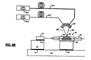
- FIGs. 6A and 6B illustrate the optical connection module of FIG. 2 and exemplary laser soldering systems
- FIGs. 7A and 7B illustrate an integrated optical connection module with a laser and an optical component such as an optical fiber according to the present invention
- FIGs. 8A-8C illustrate a first embodiment of the integrated optical connection module of FIG. 7;
- FIGs. 9A-9C illustrate the use of glass frit in lateral gaps of the first embodiment of the integrated optical connection module of FIG. 7;
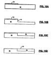
- FIGs. 10A-10D illustrate a second embodiment of the integrated optical connection module of FIG. 7.
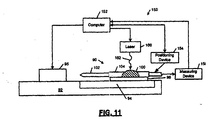
- FIG. 11 illustrates optical component alignment system according to the present invention.
- the present invention discloses apparatus and an improved method for attaching an optical component to a substrate aligning the optical component to a laser.
- Skilled artisans will appreciate that the present invention can be employed to attach active and passive optical components such as optical fiber, mirrors, lenses, detectors, microelectromechanical (MEMS) devices, isolators and other optical components to a substrate without causing damage to the laser due to heat.
- active and passive optical components such as optical fiber, mirrors, lenses, detectors, microelectromechanical (MEMS) devices, isolators and other optical components
- a laser 32 is attached to a laser submount 38 by a bonding region 40.
- the laser submount 38 is connected to a substrate 42 by a bonding region 44.
- An optical fiber 34 is attached to a fiber bonding pad 50 by solder 52.
- the fiber bonding pad 50 can include one or more layers. At least one of the layers is preferably metallic.
- the optical fiber 34 preferably has a metallic outer layer 53 along a portion of the optical fiber 34 for bonding with the solder 52. Alternately, the metallic outer layer 53 can be omitted and the solder can be flowed completely around the optical fiber 34 to attach the optical fiber 34 to the fiber bonding pad 50. Suitable metallic outer layers 53 may be NiAu and other similar metallic layers.
- An end of the optical fiber 34 may include a lensed surface 54 to increase the coupling efficiency of the optical fiber 34.
- the fiber bonding pad 50 is attached to a fiber submount 55.
- the fiber submount 55 is attached by a bonding region 56 to the substrate 42.
- the solder 52 preferably has a relatively high melting temperature such as 250°C or higher.
- the solder is eutectic and hard with minimal creep at room temperature. Creep is a function of activation energy that is typically related to the melting temperature of the solder. In other words, a high melting temperature generally corresponds to high activation energy. Minimizing creep helps maintain alignment in use.
- the solder can be AuSn and have a melting temperature of 284°C. Composition percentages such as 80% - Au and 20% - Sn or other compositions are also contemplated. Other suitable solder materials include PbSn and AuGe.
- the fiber submount 55 is preferably made of a thermally insulating material.
- the thermally insulating material can be glass (silicon dioxide (SiO 2 )), ceramic such as Micor, Zirconia or M120, or any other similar thermally insulating material.
- the path between the laser 32 and the substrate 42 preferably has a relatively high thermal conductivity.
- the laser submount 38 and the bonding regions 40 and 44 have a relatively high thermal conductivity to minimize the laser junction temperature during operation and to improve the power, efficiency and reliability.
- the laser submount 38 is preferably formed from CuW, AIN, SiC, BeO, Si, TcBN, or diamond.
- the bonding regions 40 and 44 preferably include solder such as AuSn with 80% Au and 20% Sn (other compositions and percentages are also contemplated).
- the fiber bonding pad 50 includes one or more layers and provides lateral heat conduction to adequately conduct heat to the solder 52 during laser soldering.
- the fiber submount 55 limits vertical heat conduction to prevent heat flow through the fiber bonding pad 50 and the fiber submount 55 to the substrate 42 and the laser 32.
- the fiber bonding pad 50 also provides a solder dam, absorbs laser light, increases robustness of the attachment region and/or fosters lateral heat conduction.
- the fiber bonding pad 50 includes layers 60a through 60h.
- Layer 60a provides a solder wetting layer and is preferably made of Au or other similar materials.
- Layer 60b provides a solder barrier and is preferably made of Pt or other similar materials.
- Layer 60c provides a mechanical support and is preferably made of Ni or other similar materials.
- Layer 60d provides an adhesion between layers 60c and 60e and is preferably made of Ti or other similar materials.
- Layer 60e provides for absorption of the incident laser light, acts as a solder barrier and is preferably made of Ti or other similar materials.
- Layer 60f provides for lateral conduction of heat and is preferably made of Ni or other similar materials.
- Layer 60g provides an adhesion between layers 60f and 60h and is preferably made of Ti or other similar materials.
- Layer 60h provides for lateral conduction and adhesion to fiber submount 55 and is preferably made of Ni-ceramic composite or other similar materials.
- the fiber bonding pad 50 provides a robust attachment point to the fiber mount and a solder barrier.
- the fiber bonding pad 50 also should allow lateral heat conduction through the thickness of the layer(s) provided by the fiber bonding pad 50.
- the solder 52 is preferably melted during the alignment and attachment process using laser heating.
- a laser source 70 is connected to an optical fiber 74.
- a beam of light 76 is output by the optical fiber 74.
- the beam of light 76 is collimated by a collimating lens 78 and focused by a focusing lens 80 onto the solder 52.
- the required power of the laser source 70 is relatively low, for example 1-3 Watts (W) is typically sufficient when AuSn is employed as solder 52.
- W Watts
- the beam of light 76 is turned off or directed away from the solder 52.
- the solder 52 cools, solidifies, and fixes the position of the optical fiber 34 relative to the laser 32.
- multiple laser sources 82-1 and 82-2 are connected by optical fibers 84-1 and 84-2 to a beam delivery system 86.
- the beam delivery system 86 directs the beams of light 88 onto the solder 52 during the alignment and attachment process.
- the process of alignment may be repeated one or more times until alignment is achieved. As can be appreciated, more than two laser sources may be employed if desired.
- the integrated optical connection module 90 includes a substrate 92 and a thermally insulating material 94 that is integrated directly into the substrate 92.
- the substrate 92 is preferably fabricated from silicon, InP, GaAs or other suitable materials.
- the thermally insulating material 94 is preferably glass, ceramic, or any other suitable thermally insulating material.
- the thermally insulating material 94 is planar.
- a fiber bonding pad 96 is attached to a top surface of the thermally insulating material 94.
- the fiber bonding pad 96 is preferably similar in structure to the fiber bonding pad 50.
- a laser 95 is fabricated directly on the substrate 92 or is attached using a bonding region (not shown).
- Solder 100 attaches an optical fiber 102 to the fiber bonding pad 96.
- An optional metallic outer layer 104 (as discussed above) may be employed.
- a laser heats the solder 102 and/or heats the fiber bonding pad 96.
- FIG. 7A a single beam 106 of laser light heats the solder 100.
- FIG. 7B multiple beams 107 and 108 of laser light uniformly heat the fiber bonding pad 96.
- a first method for fabricating the relatively thick thermally insulating material 94 in the substrate 92 is shown.
- the substrate 92 and the thermally insulating material 94 are patterned and etched.
- the smoothness of the bonding surfaces of the substrate 92 and the thermally insulating material 94 should approximately match.
- the material used to form the substrate 92 and the thermally insulating material have coefficients of thermal expansion (CTE) that approximately match.
- the substrate 92 and the thermally insulating material 94 are initially brought into contact at an elevated temperature in the presence of an electric field. An anodic bond is formed between the substrate 92 in the thermally insulating material 94 at the atomic scale.
- the substrate 92 and the thermally insulating material 94 are polished in FIG. 8C.
- the foregoing method allows the integration of the relatively thick thermally insulating material 94 with the substrate 92.
- thermally insulating material 94 and the substrate 92 have etched features or lateral gaps 110 between edges 112 of the thermally insulating material 94 and edges 114 of the substrate 92.
- the gaps 100 are filled with glass frit 116 in a powder form as is shown in FIG. 9B.
- the glass frit 116 solidifies into glass.
- a top surface 118 is polished to provide a planar, smooth surface as illustrated in FIG. 9C. Annealing is performed at temperatures in excess of 300°C.
- FIGs. 10A, 10B, 10C, and 10D a second method for fabricating the integrated fiber-coupled laser module 90 is shown.
- the substrate 92 is patterned using a mask 120.
- the substrate 92 is etched at 93.
- reactive ion etching, chemical etching, or other suitable etching methods are employed.
- the mask 120 is removed and a thermally insulating material 122 is formed by one or more flame-hydrolysis growths. Typically, 10-30 micron layers are added per growth.
- polishing is performed to re-expose the substrate 92 in regions where previously covered by mask 120 to provide a planar, smooth top surface 124.
- the materials that are selected for the substrate 92 and the thermally insulating material 94 have CTEs that approximately match. Creating the thermally insulating material 94 using flame-hydrolysis provides void-free adhesion of glass onto the substrate 92.
- the integrated optical connection module 90 has excellent planarity.
- the thickness of the thermally insulating material 94 is preferably between 20 and 300 micrometers.
- the optical connection modules according to the present invention have high thermal conductivity between the laser and the substrate to enable high-power operation.
- the optical connection modules also have high thermal insulation between the optical fiber attachment region and the laser to minimize temperature increase of the laser during solder attachment of the optical fiber.
- the optical connection modules have relatively high thermal conductivity in the fiber attachment region to minimize the required heat.
- the optical connection modules are mechanically stable over the operating and processing temperatures.
- the integrated optical connection modules are planar and relatively low-cost to fabricate.
- an optical component alignment system 150 is illustrated and includes a computer 152, a positioning device 154, and a measuring device 158.
- the optical component alignment system 150 is shown in conjunction with the embodiment of FIG. 7A. Skilled artisans will appreciate that the optical component alignment system 150 can be used with other embodiments disclosed herein.
- a laser 160 generates one or more beams 162 of laser light that are directed at the solder 100 and/or the fiber bonding pad 96 to heat the solder.
- the computer 152 turns on the laser 95.
- the measuring device 158 generates an output signal related to the output of the optical fiber 102 or other optical component and outputs the output signal to the computer 152.
- the computer 152 calculates position adjustment signals that are used to adjust the position of the optical fiber 102. One or more iterations are performed until the optical fiber 102 is properly aligned with the laser 95.
Landscapes
- Physics & Mathematics (AREA)
- General Physics & Mathematics (AREA)
- Optics & Photonics (AREA)
- Condensed Matter Physics & Semiconductors (AREA)
- Electromagnetism (AREA)
- Optical Couplings Of Light Guides (AREA)
- Semiconductor Lasers (AREA)
Abstract
Description
- The present invention relates to optical fibers, and more particularly to the attachment of optical components to a substrate and to the alignment of the optical component to a laser.
- There is a significant and growing demand in the optoelectronics industry for low cost fiber-coupled laser modules that are highly reliable. Fiber-coupled laser modules include an optical fiber that is aligned with a laser on a substrate and that is attached to the substrate. Single mode fiber devices require fiber-coupled laser modules. For example, fiber-coupled laser modules are used in pumps for fiber amplifiers, wavelength division multiplex (WDM) sources, high-speed and high-power distributed feedback (DFB) lasers, and semiconductor optical amplifiers.
- Generally, the laser and the optical fiber are fabricated or mounted on a substrate. To achieve acceptable performance, the optical fiber must be precisely aligned to the laser. After alignment, the optical fiber must be securely attached to the substrate without adversely impacting alignment, damaging the laser or the optical fiber, or turning the laser off. Proper alignment ensures that the optical interface has a very high single mode coupling efficiency. The connection between the optical fiber and the substrate must also be capable of withstanding environmental conditions such as operating temperature variations, vibration, dust, etc. Other important attributes include a relatively high thermal conductivity between the laser and the substrate to allow high power operation of the laser.
- The high thermal conductivity between the laser and the substrate may cause problems when connecting the optical fiber to the substrate using attachment methods that employ heat. For example, soldering is often used to attach the optical fiber to the substrate. Soldering involves heating the metallic parts that are to be connected together and using solder to bind the parts together. Oftentimes, an integrated resistor that is in a heat exchange relationship with the solder is used as a heat source for melting the solder.
- Referring now to FIG. 1, a fiber-coupled
laser module 10 according to the prior art includes alaser 12 and anoptical fiber 14 that are attached to asubstrate 16. Heat (identified by arrows 18) is generated during attachment of theoptical fiber 14 to thesubstrate 16 usingsolder 20. Most of theheat 18 from the soldering operation tends to flow downward through thesubstrate 16 to a heatsink (not shown) such as a thermoelectric cooler (TEC). Due to the relatively high thermal conductivity of the path between thelaser 12 and thesubstrate 16, some of the heat 18' is also conducted to thelaser 12. The heat 18' may damage the diode or melt the solder that connects thelaser 12 to thesubstrate 16, which decreases the reliability of thelaser 12 and increases degradation of the solder connection. The heat 18' can also cause misalignment of thelaser 12 and/or turn off thelaser 12 during alignment. - An optical connection module according to the invention attaches an optical component to a substrate and aligns the optical component to a laser. The optical connection module includes a fiber submount that is attached to the substrate and a thermally insulating material having a thickness greater than 20 micrometers. An optical component is soldered to the fiber submount by application of heat from a laser. A laser submount is attached to the substrate. A laser is attached to the laser submount.
- In other features of the invention, the optical component is selected from active and passive optical components such as optical fiber, lenses, mirrors, filters, detectors, isolators, and microelectromechanical devices.
- In still other features of the invention, a fiber bonding pad is located between the solder and the thermally insulating material. The fiber bonding pad has a lateral heat flow characteristic that is significantly greater than its vertical heat flow characteristic. The fiber bonding pad is located between the thermally insulating material and the optical fiber. The fiber bonding pad and the thermally insulating material conduct heat locally and laterally during laser soldering to uniformly melt the solder. The thermally insulating material and the fiber bonding pad limit heat transfer to the substrate during soldering. The fiber bonding pad also provides a robust attachment location for connecting the optical component. The thickness of the fiber bonding pad also helps conduct heat laterally. The fiber bonding pad also provides a solder dam.
- In yet other features of the invention, the fiber bonding pad includes multiple layers. One layer is made of Au and another layer is selected from the group of Ni, Cr, Ti and CrO. Additional layers can be made of Ti and Pt.
- In another feature of the invention, an integrated fiber-coupled laser module for aligning and attaching an optical fiber to a substrate includes a thermally insulating material formed integrally in the substrate and having a thickness greater than 20 micrometers. A fiber bonding pad includes at least one metallic layer attached to the thermally insulating material. An optical fiber is laser soldered to the fiber bonding pad. A laser is located on the substrate.
- In still other features of the invention, the integrated thermally insulating material is formed by flame hydrolysis or by anodic bonding.
- Further areas of applicability of the present invention will become apparent from the detailed description provided hereinafter. It should be understood that the detailed description and specific examples, while indicating the preferred embodiment of the invention, are intended for purposes of illustration only and are not intended to limit the scope of the invention.
- The present invention will become more fully understood from the detailed description and the accompanying drawings, wherein:
- FIG. 1 illustrates a fiber-coupled laser module with a laser and an optical fiber that are aligned and attached to a substrate according to the prior art;
- FIG. 2 illustrates an optical connection module with a laser and an optical component such as an optical fiber that are attached to a substrate according to the present invention;
- FIG. 3 is a side cross-section that illustrates a fiber bonding pad that is located between the optical component and an insulating fiber submount;
- FIG. 4 is a plan view that illustrates part of the fiber bonding pad;
- FIG. 5 is an end cross-section that illustrates the solder and part of the fiber bonding pad;
- FIGs. 6A and 6B illustrate the optical connection module of FIG. 2 and exemplary laser soldering systems;
- FIGs. 7A and 7B illustrate an integrated optical connection module with a laser and an optical component such as an optical fiber according to the present invention;
- FIGs. 8A-8C illustrate a first embodiment of the integrated optical connection module of FIG. 7;
- FIGs. 9A-9C illustrate the use of glass frit in lateral gaps of the first embodiment of the integrated optical connection module of FIG. 7;
- FIGs. 10A-10D illustrate a second embodiment of the integrated optical connection module of FIG. 7; and
- FIG. 11 illustrates optical component alignment system according to the present invention.
- The following description of the preferred embodiment(s) is merely exemplary in nature and is in no way intended to limit the invention, its application, or uses.
- The present invention discloses apparatus and an improved method for attaching an optical component to a substrate aligning the optical component to a laser. Skilled artisans will appreciate that the present invention can be employed to attach active and passive optical components such as optical fiber, mirrors, lenses, detectors, microelectromechanical (MEMS) devices, isolators and other optical components to a substrate without causing damage to the laser due to heat.
- Referring now to FIG. 2, the present invention will be described in the context of an
optical connection module 30 for an optical fiber. Skilled artisans will appreciate that the present invention applies to the attachment and the alignment of other active and passive optical components. Alaser 32 is attached to alaser submount 38 by abonding region 40. Thelaser submount 38 is connected to asubstrate 42 by abonding region 44. Anoptical fiber 34 is attached to afiber bonding pad 50 bysolder 52. Thefiber bonding pad 50 can include one or more layers. At least one of the layers is preferably metallic. - The
optical fiber 34 preferably has a metallic outer layer 53 along a portion of theoptical fiber 34 for bonding with thesolder 52. Alternately, the metallic outer layer 53 can be omitted and the solder can be flowed completely around theoptical fiber 34 to attach theoptical fiber 34 to thefiber bonding pad 50. Suitable metallic outer layers 53 may be NiAu and other similar metallic layers. An end of theoptical fiber 34 may include a lensed surface 54 to increase the coupling efficiency of theoptical fiber 34. Thefiber bonding pad 50 is attached to afiber submount 55. Thefiber submount 55 is attached by abonding region 56 to thesubstrate 42. - The
solder 52 preferably has a relatively high melting temperature such as 250°C or higher. Preferably, the solder is eutectic and hard with minimal creep at room temperature. Creep is a function of activation energy that is typically related to the melting temperature of the solder. In other words, a high melting temperature generally corresponds to high activation energy. Minimizing creep helps maintain alignment in use. For example, the solder can be AuSn and have a melting temperature of 284°C. Composition percentages such as 80% - Au and 20% - Sn or other compositions are also contemplated. Other suitable solder materials include PbSn and AuGe. Thefiber submount 55 is preferably made of a thermally insulating material. For example, the thermally insulating material can be glass (silicon dioxide (SiO2)), ceramic such as Micor, Zirconia or M120, or any other similar thermally insulating material. - The path between the
laser 32 and thesubstrate 42 preferably has a relatively high thermal conductivity. In other words, thelaser submount 38 and thebonding regions laser submount 38 is preferably formed from CuW, AIN, SiC, BeO, Si, TcBN, or diamond. Thebonding regions - Referring now to FIG. 3, a preferred embodiment of the
fiber bonding pad 50 andfiber submount 55 is shown in further detail. Thefiber bonding pad 50 includes one or more layers and provides lateral heat conduction to adequately conduct heat to thesolder 52 during laser soldering. Thefiber submount 55 limits vertical heat conduction to prevent heat flow through thefiber bonding pad 50 and thefiber submount 55 to thesubstrate 42 and thelaser 32. Thefiber bonding pad 50 also provides a solder dam, absorbs laser light, increases robustness of the attachment region and/or fosters lateral heat conduction. - In one embodiment, the
fiber bonding pad 50 includes layers 60a through 60h. Layer 60a provides a solder wetting layer and is preferably made of Au or other similar materials. Layer 60b provides a solder barrier and is preferably made of Pt or other similar materials. Layer 60c provides a mechanical support and is preferably made of Ni or other similar materials. Layer 60d provides an adhesion between layers 60c and 60e and is preferably made of Ti or other similar materials. Layer 60e provides for absorption of the incident laser light, acts as a solder barrier and is preferably made of Ti or other similar materials. Layer 60f provides for lateral conduction of heat and is preferably made of Ni or other similar materials. Layer 60g provides an adhesion between layers 60f and 60h and is preferably made of Ti or other similar materials. Layer 60h provides for lateral conduction and adhesion tofiber submount 55 and is preferably made of Ni-ceramic composite or other similar materials. - The
fiber bonding pad 50 provides a robust attachment point to the fiber mount and a solder barrier. Thefiber bonding pad 50 also should allow lateral heat conduction through the thickness of the layer(s) provided by thefiber bonding pad 50. As can be appreciated, there are many variations that may be readily apparent to those skilled in the art, including removal of one or more of the layers, the addition of other layers, and/or substitution of layers with similar properties. - Referring now to FIG. 6A, the
solder 52 is preferably melted during the alignment and attachment process using laser heating. For purposes of clarity, reference numbers from FIG. 2 are used in FIG. 6A where appropriate to identify the same elements. A laser source 70 is connected to anoptical fiber 74. A beam oflight 76 is output by theoptical fiber 74. The beam oflight 76 is collimated by a collimatinglens 78 and focused by a focusinglens 80 onto thesolder 52. Advantageously, the required power of the laser source 70 is relatively low, for example 1-3 Watts (W) is typically sufficient when AuSn is employed assolder 52. Initially thelaser 32 and theoptical fiber 34 are aligned. The beam of light 76 heats thesolder 52 causing thesolder 52 to melt. The beam oflight 76 is turned off or directed away from thesolder 52. Thesolder 52 cools, solidifies, and fixes the position of theoptical fiber 34 relative to thelaser 32. Referring now to FIG. 6B, multiple laser sources 82-1 and 82-2 are connected by optical fibers 84-1 and 84-2 to abeam delivery system 86. Thebeam delivery system 86 directs the beams of light 88 onto thesolder 52 during the alignment and attachment process. The process of alignment may be repeated one or more times until alignment is achieved. As can be appreciated, more than two laser sources may be employed if desired. - Referring now to FIGs. 7A and 7B, an integrated
optical connection module 90 is shown. The integratedoptical connection module 90 includes asubstrate 92 and a thermally insulatingmaterial 94 that is integrated directly into thesubstrate 92. Thesubstrate 92 is preferably fabricated from silicon, InP, GaAs or other suitable materials. The thermally insulatingmaterial 94 is preferably glass, ceramic, or any other suitable thermally insulating material. The thermally insulatingmaterial 94 is planar. Afiber bonding pad 96 is attached to a top surface of the thermally insulatingmaterial 94. Thefiber bonding pad 96 is preferably similar in structure to thefiber bonding pad 50. Alaser 95 is fabricated directly on thesubstrate 92 or is attached using a bonding region (not shown).Solder 100 attaches anoptical fiber 102 to thefiber bonding pad 96. An optional metallic outer layer 104 (as discussed above) may be employed. A laser heats thesolder 102 and/or heats thefiber bonding pad 96. In FIG. 7A, a single beam 106 of laser light heats thesolder 100. In FIG. 7B,multiple beams fiber bonding pad 96. - Referring now to FIGs. 8A, 8B and 8C, a first method for fabricating the relatively thick thermally insulating
material 94 in thesubstrate 92 is shown. Thesubstrate 92 and the thermally insulatingmaterial 94 are patterned and etched. The smoothness of the bonding surfaces of thesubstrate 92 and the thermally insulatingmaterial 94 should approximately match. Preferably, the material used to form thesubstrate 92 and the thermally insulating material have coefficients of thermal expansion (CTE) that approximately match. Thesubstrate 92 and the thermally insulatingmaterial 94 are initially brought into contact at an elevated temperature in the presence of an electric field. An anodic bond is formed between thesubstrate 92 in the thermally insulatingmaterial 94 at the atomic scale. Thesubstrate 92 and the thermally insulatingmaterial 94 are polished in FIG. 8C. As can be appreciated, the foregoing method allows the integration of the relatively thick thermally insulatingmaterial 94 with thesubstrate 92. - Referring now to FIGs. 9A, 9B, and 9C, additional steps for fabricating the relatively thick thermally insulating
material 94 in thesubstrate 92 are shown. The thermally insulatingmaterial 94 and thesubstrate 92 have etched features orlateral gaps 110 betweenedges 112 of the thermally insulatingmaterial 94 andedges 114 of thesubstrate 92. Thegaps 100 are filled withglass frit 116 in a powder form as is shown in FIG. 9B. After high-temperature annealing, theglass frit 116 solidifies into glass. Atop surface 118 is polished to provide a planar, smooth surface as illustrated in FIG. 9C. Annealing is performed at temperatures in excess of 300°C. - Referring now to FIGs. 10A, 10B, 10C, and 10D, a second method for fabricating the integrated fiber-coupled
laser module 90 is shown. In FIG. 10A, thesubstrate 92 is patterned using amask 120. In FIG. 10B, thesubstrate 92 is etched at 93. Preferably, reactive ion etching, chemical etching, or other suitable etching methods are employed. In FIG. 10C, themask 120 is removed and a thermally insulating material 122 is formed by one or more flame-hydrolysis growths. Typically, 10-30 micron layers are added per growth. - In FIG. 10D, polishing is performed to re-expose the
substrate 92 in regions where previously covered bymask 120 to provide a planar, smoothtop surface 124. Preferably, the materials that are selected for thesubstrate 92 and the thermally insulatingmaterial 94 have CTEs that approximately match. Creating the thermally insulatingmaterial 94 using flame-hydrolysis provides void-free adhesion of glass onto thesubstrate 92. In addition, the integratedoptical connection module 90 has excellent planarity. - The thickness of the thermally insulating
material 94 is preferably between 20 and 300 micrometers. The optical connection modules according to the present invention have high thermal conductivity between the laser and the substrate to enable high-power operation. The optical connection modules also have high thermal insulation between the optical fiber attachment region and the laser to minimize temperature increase of the laser during solder attachment of the optical fiber. The optical connection modules have relatively high thermal conductivity in the fiber attachment region to minimize the required heat. In addition, the optical connection modules are mechanically stable over the operating and processing temperatures. The integrated optical connection modules are planar and relatively low-cost to fabricate. - Referring now to FIG. 11, an optical component alignment system 150 is illustrated and includes a
computer 152, apositioning device 154, and a measuring device 158. The optical component alignment system 150 is shown in conjunction with the embodiment of FIG. 7A. Skilled artisans will appreciate that the optical component alignment system 150 can be used with other embodiments disclosed herein. - A
laser 160 generates one ormore beams 162 of laser light that are directed at thesolder 100 and/or thefiber bonding pad 96 to heat the solder. Thecomputer 152 turns on thelaser 95. The measuring device 158 generates an output signal related to the output of theoptical fiber 102 or other optical component and outputs the output signal to thecomputer 152. Thecomputer 152 calculates position adjustment signals that are used to adjust the position of theoptical fiber 102. One or more iterations are performed until theoptical fiber 102 is properly aligned with thelaser 95. - Those skilled in the art can now appreciate from the foregoing description that the broad teachings of the present invention can be implemented in a variety of forms. Therefore, while this invention has been described in connection with particular examples thereof, the true scope of the invention should not be so limited since other modifications will become apparent to the skilled practitioner upon a study of the drawings, the specification and the following claims.
Claims (13)
- An optical connection module for attaching an optical component to a substrate and aligning said optical component with a first laser, comprising:a substrate;a fiber submount attached to said substrate including a thermally insulating material having a thickness greater than 20 micrometers;an optical component soldered to said fiber submount using heat from a second laser;a laser submount attached to said substrate; anda laser attached to said laser submount.
- The optical connection module of claim 1 wherein said optical connection module is a fiber-coupled laser module and said optical component is an optical fiber.
- The optical connection module of claim I further comprising a fiber bonding pad located between said thermally insulating material and said optical component.
- The optical connection module of claim 1 wherein said fiber bonding pad and said thermally insulating material conduct heat locally during soldering to uniformly melt said solder limit heat transfer to said substrate.
- The optical connection module of claim 3, wherein said fiber bonding pad performs at least one of providing a solder dam, absorbing laser light, laterally conducting heat, and improving the strength of an attachment between said optical component and said substrate.
- The laser module of claim 5, wherein said fiber bonding pad comprises a plurality of layers including,
a first layer of Au;
a second layer selected from the group of Ni, Cr, Ti and CrO;
third layer of Ti; and
a fourth layer of Pt. - The optical connection module of claim 1 wherein,
said thermally insulating material is selected from the group of glass and ceramic; said solder is selected from the group of AuSn, PbSn and AuGe; and,
said laser submount is selected from the group of AlN, AlNi, SiC, BeO, TcBN, diamond and Si. - The optical connection module of claim 1 wherein said optical component is selected from the group of optical fiber, mirrors, lenses, detectors, microelectromechanical (MEMS) devices, and isolators.
- A method of fabricating an integrated optical connection module, comprising:providing a substrate;patterning and etching a first region of said substrate;providing a thermally insulating material in said first region of said substrate;polishing said thermally insulating material and said substrate to provide a planar surface including a substrate portion and a thermally insulating portion;attaching a fiber bonding pad including at least one metallic layer to said thermally insulating portion;locating a first laser on said substrate portion; andaligning and attaching an optical component to said fiber bonding pad.
- The method of claim 9, wherein said thermally insulating material is provided by anodic bonding.
- The method of claim 10, wherein at least one lateral gap is formed between said substrate and said thermally insulating material, further comprising the steps of:filling said lateral gap with glass frit;annealing said substrate, said thermally insulating material and said glass frit; andpolishing a top surface of said substrate, said thermally insulating material and said glass frit.
- The method of claim 9, wherein said thermally insulating material is provided by flame hydrolysis in said first region.
- The method of claim 9, wherein said optical component is attached to said fiber bonding pad using solder that is heated using a laser.
Applications Claiming Priority (2)
| Application Number | Priority Date | Filing Date | Title |
|---|---|---|---|
| US16473 | 2001-12-10 | ||
| US10/016,473 US6758610B2 (en) | 2001-12-10 | 2001-12-10 | Optical component attachment to optoelectronic packages |
Publications (3)
| Publication Number | Publication Date |
|---|---|
| EP1328047A2 true EP1328047A2 (en) | 2003-07-16 |
| EP1328047A3 EP1328047A3 (en) | 2006-09-27 |
| EP1328047B1 EP1328047B1 (en) | 2009-10-07 |
Family
ID=21777313
Family Applications (1)
| Application Number | Title | Priority Date | Filing Date |
|---|---|---|---|
| EP02258425A Expired - Lifetime EP1328047B1 (en) | 2001-12-10 | 2002-12-06 | Optical component attachment to optoelectronic packages |
Country Status (5)
| Country | Link |
|---|---|
| US (1) | US6758610B2 (en) |
| EP (1) | EP1328047B1 (en) |
| CN (1) | CN1275062C (en) |
| DE (1) | DE60233927D1 (en) |
| RU (1) | RU2304294C2 (en) |
Families Citing this family (33)
| Publication number | Priority date | Publication date | Assignee | Title |
|---|---|---|---|---|
| CA2509530C (en) * | 2002-12-10 | 2013-07-23 | Picometrix, Inc. | Precision optical fiber attachment using solder glass preform |
| US20050007118A1 (en) * | 2003-04-09 | 2005-01-13 | John Kitching | Micromachined alkali-atom vapor cells and method of fabrication |
| US20040232535A1 (en) * | 2003-05-22 | 2004-11-25 | Terry Tarn | Microelectromechanical device packages with integral heaters |
| US20040245228A1 (en) * | 2003-06-04 | 2004-12-09 | Hongwei Liu | Attach aligned optics and microelectronics with laser soldering methods |
| US7284913B2 (en) * | 2003-07-14 | 2007-10-23 | Matsushita Electric Industrial Co., Ltd. | Integrated fiber attach pad for optical package |
| US7146083B2 (en) * | 2004-03-31 | 2006-12-05 | Imra America, Inc. | Etched plate alignment method and apparatus |
| US7293922B2 (en) * | 2004-06-02 | 2007-11-13 | Matsushita Electric Industrial Co., Ltd. | Non-mechanical adjustment of an optical fiber to an optical output port |
| DE102004057454B4 (en) * | 2004-11-25 | 2009-10-22 | Jenoptik Laserdiode Gmbh | Diode laser module and method for its production |
| US7691723B2 (en) * | 2005-01-07 | 2010-04-06 | Honeywell International Inc. | Bonding system having stress control |
| EP1942358A2 (en) | 2006-12-27 | 2008-07-09 | JDS Uniphase Corporation | Component assembly and fabrication method |
| US7512306B2 (en) | 2007-01-03 | 2009-03-31 | Jds Uniphase Corporation | Polarization maintaining fiber pigtail assembly |
| US20100303109A1 (en) * | 2009-05-26 | 2010-12-02 | Venkata Adiseshaiah Bhagavatula | Proximity Coupled Athermal Optical Package Comprising Laser Source And Compound Facet Wavelength Conversion Device |
| US8102887B2 (en) * | 2009-05-26 | 2012-01-24 | Corning Incorporated | Edge bonded optical packages |
| US8475056B2 (en) * | 2009-07-28 | 2013-07-02 | Jds Uniphase Corporation | Semiconductor device assembly |
| US8111452B2 (en) * | 2010-02-22 | 2012-02-07 | Corning Incorporated | Wavelength conversion device with microlens and optical package incorporating the same |
| WO2011122440A1 (en) | 2010-03-30 | 2011-10-06 | 株式会社フジクラ | Laser device and method for manufacturing same |
| CN102844943A (en) * | 2010-03-31 | 2012-12-26 | 株式会社藤仓 | Laser device |
| JP5508249B2 (en) * | 2010-12-21 | 2014-05-28 | 株式会社フジクラ | Manufacturing method of optical module |
| JP5102380B2 (en) * | 2011-02-24 | 2012-12-19 | 株式会社フジクラ | Fiber mount device, optical module using the same, and method of manufacturing optical module |
| JP2013004752A (en) | 2011-06-16 | 2013-01-07 | Fujikura Ltd | Laser module |
| JP5281122B2 (en) * | 2011-06-16 | 2013-09-04 | 株式会社フジクラ | Joining method and manufacturing method |
| CN102412500A (en) * | 2011-11-30 | 2012-04-11 | 江苏飞格光电有限公司 | Packaging method of semiconductor laser |
| JP5230829B1 (en) | 2012-03-09 | 2013-07-10 | 株式会社フジクラ | Moisture removal method, optical fiber soldering method, and semiconductor laser module manufacturing method |
| WO2015012694A1 (en) * | 2013-07-24 | 2015-01-29 | Effect Photonics B.V. | Optical subassembly, optical system and method |
| JP6488539B2 (en) * | 2013-11-27 | 2019-03-27 | 住友大阪セメント株式会社 | Optical element module |
| CN104070282B (en) * | 2014-06-30 | 2016-05-04 | 北京航天时代光电科技有限公司 | A kind of photodetector pigtail coupling welder and method |
| WO2016007860A1 (en) * | 2014-07-11 | 2016-01-14 | Acacia Communications, Inc. | Integrated high-power tunable laser with adjustable outputs |
| JP2021521674A (en) * | 2018-04-06 | 2021-08-26 | アイピージー フォトニクス コーポレーション | Underwater optical repeater with high voltage insulation |
| US11137581B2 (en) * | 2018-09-27 | 2021-10-05 | Himax Technologies Limited | Wafer-level homogeneous bonding optical structure and method to form the same |
| US10809469B1 (en) * | 2019-04-02 | 2020-10-20 | Cloud Light Technology Limited | Laser diode edge assembly structure for three-dimensional active alignment in transmitter optical assembly |
| WO2021003306A1 (en) * | 2019-07-02 | 2021-01-07 | Aayuna Inc. | Laser engine supporting multiple laser sources |
| WO2022266786A1 (en) * | 2021-06-21 | 2022-12-29 | Lumentum Operations Llc | Control of solder bond line thickness with squeezed gold bump space |
| US20230408767A1 (en) * | 2022-06-17 | 2023-12-21 | Ayar Labs, Inc. | High-Temperature-Compatible Fiber Array Packaging Methods |
Citations (1)
| Publication number | Priority date | Publication date | Assignee | Title |
|---|---|---|---|---|
| JPS62211965A (en) | 1986-03-13 | 1987-09-17 | Toshiba Corp | Photosemiconductor device |
Family Cites Families (23)
| Publication number | Priority date | Publication date | Assignee | Title |
|---|---|---|---|---|
| JPS57138191A (en) * | 1981-02-19 | 1982-08-26 | Kokusai Denshin Denwa Co Ltd <Kdd> | United structure of semiconductor laser and optical fiber |
| SU1263078A1 (en) * | 1984-10-24 | 1996-10-10 | С.А. Алавердян | Device for optical integration of light guide and light-emitting or light-receiving element |
| GB8508280D0 (en) | 1985-03-29 | 1985-05-09 | British Telecomm | Optical component mounting |
| FR2582413B1 (en) * | 1985-05-23 | 1988-12-02 | Comp Generale Electricite | METHOD FOR COUPLING AN OPTICAL FIBER TO AN OPTOELECTRONIC COMPONENT ON A BASE |
| US4708429A (en) | 1985-09-26 | 1987-11-24 | Rca Corporation | Optical fiber assembly and optically coupled device package including same |
| US4702547A (en) | 1986-07-28 | 1987-10-27 | Tektronix, Inc. | Method for attaching an optical fiber to a substrate to form an optical fiber package |
| FR2605418B1 (en) * | 1986-10-17 | 1990-04-20 | Thomson Semiconducteurs | MODULE FOR COUPLING BETWEEN A SEMICONDUCTOR DEVICE AND AN OPTICAL FIBER, AND METHOD FOR ALIGNING THE SEMICONDUCTOR DEVICE AND THE FIBER |
| JPH01118106A (en) | 1987-10-30 | 1989-05-10 | Japan Aviation Electron Ind Ltd | Method for centering and fixing optical fiber |
| FR2623297B1 (en) | 1987-11-13 | 1991-09-27 | Cit Alcatel | COUPLING DEVICE BETWEEN AN OPTICAL FIBER AND AN OPTOELECTRONIC COMPONENT |
| US4997253A (en) | 1989-04-03 | 1991-03-05 | Tektronix, Inc. | Electro-optical transducer module and a method of fabricating such a module |
| US4971418A (en) | 1989-08-31 | 1990-11-20 | At&T Bell Laboratories | Apparatus and method for making low-loss permanent optical fiber splices |
| US4970365A (en) | 1989-09-28 | 1990-11-13 | International Business Machines Corporation | Method and apparatus for bonding components leads to pads located on a non-rigid substrate |
| EP0584356B1 (en) | 1992-01-17 | 1996-06-26 | S.L.T. Japan Co, Ltd. | Method of soldering |
| US5307434A (en) | 1992-07-16 | 1994-04-26 | At&T Bell Laboratories | Article that comprises a laser coupled to an optical fiber |
| US5359686A (en) | 1993-03-29 | 1994-10-25 | Motorola, Inc. | Interface for coupling optical fibers to electronic circuitry |
| US5367140A (en) | 1993-12-27 | 1994-11-22 | At&T Bell Laboratories | Method for laser welding of optical packages |
| US5469456A (en) | 1994-03-31 | 1995-11-21 | Opto Power Corporation | Laser device and method of manufacture using non-metalized fiber |
| US5568892A (en) | 1994-06-16 | 1996-10-29 | Lucent Technologies Inc. | Alignment and bonding techniques |
| TW253856B (en) | 1994-12-13 | 1995-08-11 | At & T Corp | Method of solder bonding, and article produced by the method |
| JP3147141B2 (en) | 1995-08-30 | 2001-03-19 | 株式会社日立製作所 | Light assembly |
| US6074103A (en) | 1996-10-15 | 2000-06-13 | Sdl, Inc. | Aligning an optical fiber with electroluminescent semiconductor diodes and other optical components |
| US6205264B1 (en) * | 1998-04-14 | 2001-03-20 | Lucent Technologies Inc. | Optical assembly with improved dimensional stability |
| US6271049B1 (en) * | 1998-09-14 | 2001-08-07 | Siemens Aktiengesellschaft | Method for producing an optoelectronic component |
-
2001
- 2001-12-10 US US10/016,473 patent/US6758610B2/en not_active Expired - Lifetime
-
2002
- 2002-12-06 DE DE60233927T patent/DE60233927D1/en not_active Expired - Lifetime
- 2002-12-06 EP EP02258425A patent/EP1328047B1/en not_active Expired - Lifetime
- 2002-12-09 RU RU2002133055/28A patent/RU2304294C2/en not_active IP Right Cessation
- 2002-12-10 CN CNB021545871A patent/CN1275062C/en not_active Expired - Lifetime
Patent Citations (1)
| Publication number | Priority date | Publication date | Assignee | Title |
|---|---|---|---|---|
| JPS62211965A (en) | 1986-03-13 | 1987-09-17 | Toshiba Corp | Photosemiconductor device |
Also Published As
| Publication number | Publication date |
|---|---|
| US6758610B2 (en) | 2004-07-06 |
| US20030108304A1 (en) | 2003-06-12 |
| CN1447142A (en) | 2003-10-08 |
| DE60233927D1 (en) | 2009-11-19 |
| EP1328047A3 (en) | 2006-09-27 |
| EP1328047B1 (en) | 2009-10-07 |
| RU2304294C2 (en) | 2007-08-10 |
| CN1275062C (en) | 2006-09-13 |
Similar Documents
| Publication | Publication Date | Title |
|---|---|---|
| EP1328047B1 (en) | Optical component attachment to optoelectronic packages | |
| TWI238892B (en) | Packaging of multiple active optical devices | |
| US5857049A (en) | Precision alignment of optoelectronic devices | |
| JP3486378B2 (en) | Method for manufacturing a photoelectric device | |
| US20060239612A1 (en) | Flip-chip devices formed on photonic integrated circuit chips | |
| KR100302144B1 (en) | connector-type optical transceiver using SOI optical wave-guide | |
| JP2013080900A (en) | Light emitting module | |
| JPH10505433A (en) | Packaged optical device | |
| US10175433B2 (en) | MEMS-based levers and their use for alignment of optical elements | |
| CN101216575B (en) | Polarization maintaining fiber pigtail assembly | |
| US6582548B1 (en) | Compression bonding method using laser assisted heating | |
| JP3036446B2 (en) | Optical element mounting method | |
| US8553736B2 (en) | Laser device and method for manufacturing same | |
| JPH07199006A (en) | Optical subassembly and optical module | |
| EP1153698A1 (en) | Article comprising creep-resistant and stress-reducing solder | |
| US6184560B1 (en) | Photosemiconductor device mounted structure | |
| JP3459286B2 (en) | Lens fixing device | |
| WO2007142089A1 (en) | Optical transmission module and its manufacturing method | |
| JPH05323158A (en) | Laser diode coupling device and method for assembling the same | |
| US7021835B1 (en) | Alignment of optical components in an optical subassembly | |
| JP2001094191A (en) | Optical semiconductor module and manufacturing method thereof | |
| EP1160600A1 (en) | Semiconductor laser diode module | |
| JPH0772352A (en) | Structure for packaging flip-chip of optical semiconductor element | |
| JPH0429387A (en) | optical coupling device | |
| US6880984B2 (en) | Laser platform |
Legal Events
| Date | Code | Title | Description |
|---|---|---|---|
| PUAI | Public reference made under article 153(3) epc to a published international application that has entered the european phase |
Free format text: ORIGINAL CODE: 0009012 |
|
| AK | Designated contracting states |
Designated state(s): AT BE BG CH CY CZ DE DK EE ES FI FR GB GR IE IT LI LU MC NL PT SE SI SK TR |
|
| AX | Request for extension of the european patent |
Extension state: AL LT LV MK RO |
|
| RIN1 | Information on inventor provided before grant (corrected) |
Inventor name: DAWSON, DAVID D. Inventor name: HARGREAVES, DONALD C. Inventor name: AGRAWAL, VIVEK Inventor name: KANJAMALA, ASHOK P. Inventor name: OLESKEVICH, TANYA K. Inventor name: RANSOM, HARRISON L. Inventor name: NAGARAJAN, RADHAKRISHMAN L. Inventor name: ZIARI, MEHRDAD Inventor name: LANG, ROBERT J. |
|
| PUAL | Search report despatched |
Free format text: ORIGINAL CODE: 0009013 |
|
| AK | Designated contracting states |
Kind code of ref document: A3 Designated state(s): AT BE BG CH CY CZ DE DK EE ES FI FR GB GR IE IT LI LU MC NL PT SE SI SK TR |
|
| AX | Request for extension of the european patent |
Extension state: AL LT LV MK RO |
|
| 17P | Request for examination filed |
Effective date: 20070327 |
|
| AKX | Designation fees paid |
Designated state(s): AT BE BG |
|
| RBV | Designated contracting states (corrected) |
Designated state(s): DE FR GB |
|
| REG | Reference to a national code |
Ref country code: DE Ref legal event code: 8566 |
|
| 17Q | First examination report despatched |
Effective date: 20080312 |
|
| GRAP | Despatch of communication of intention to grant a patent |
Free format text: ORIGINAL CODE: EPIDOSNIGR1 |
|
| GRAS | Grant fee paid |
Free format text: ORIGINAL CODE: EPIDOSNIGR3 |
|
| RAP1 | Party data changed (applicant data changed or rights of an application transferred) |
Owner name: JDS UNIPHASE CORPORATION |
|
| GRAA | (expected) grant |
Free format text: ORIGINAL CODE: 0009210 |
|
| AK | Designated contracting states |
Kind code of ref document: B1 Designated state(s): DE FR GB |
|
| REG | Reference to a national code |
Ref country code: GB Ref legal event code: FG4D |
|
| REF | Corresponds to: |
Ref document number: 60233927 Country of ref document: DE Date of ref document: 20091119 Kind code of ref document: P |
|
| PGFP | Annual fee paid to national office [announced via postgrant information from national office to epo] |
Ref country code: GB Payment date: 20091123 Year of fee payment: 8 |
|
| PGFP | Annual fee paid to national office [announced via postgrant information from national office to epo] |
Ref country code: DE Payment date: 20091230 Year of fee payment: 8 |
|
| PLBE | No opposition filed within time limit |
Free format text: ORIGINAL CODE: 0009261 |
|
| STAA | Information on the status of an ep patent application or granted ep patent |
Free format text: STATUS: NO OPPOSITION FILED WITHIN TIME LIMIT |
|
| 26N | No opposition filed |
Effective date: 20100708 |
|
| PGFP | Annual fee paid to national office [announced via postgrant information from national office to epo] |
Ref country code: FR Payment date: 20110107 Year of fee payment: 9 |
|
| GBPC | Gb: european patent ceased through non-payment of renewal fee |
Effective date: 20101206 |
|
| PG25 | Lapsed in a contracting state [announced via postgrant information from national office to epo] |
Ref country code: GB Free format text: LAPSE BECAUSE OF NON-PAYMENT OF DUE FEES Effective date: 20101206 Ref country code: DE Free format text: LAPSE BECAUSE OF NON-PAYMENT OF DUE FEES Effective date: 20110701 |
|
| REG | Reference to a national code |
Ref country code: DE Ref legal event code: R119 Ref document number: 60233927 Country of ref document: DE Effective date: 20110701 |
|
| REG | Reference to a national code |
Ref country code: FR Ref legal event code: ST Effective date: 20120831 |
|
| PG25 | Lapsed in a contracting state [announced via postgrant information from national office to epo] |
Ref country code: FR Free format text: LAPSE BECAUSE OF NON-PAYMENT OF DUE FEES Effective date: 20120102 |