EP1328016A2 - Wafer-level test of integrated circuits - Google Patents
Wafer-level test of integrated circuits Download PDFInfo
- Publication number
- EP1328016A2 EP1328016A2 EP03000272A EP03000272A EP1328016A2 EP 1328016 A2 EP1328016 A2 EP 1328016A2 EP 03000272 A EP03000272 A EP 03000272A EP 03000272 A EP03000272 A EP 03000272A EP 1328016 A2 EP1328016 A2 EP 1328016A2
- Authority
- EP
- European Patent Office
- Prior art keywords
- integrated circuits
- electrode pads
- common interconnections
- common
- inspecting
- Prior art date
- Legal status (The legal status is an assumption and is not a legal conclusion. Google has not performed a legal analysis and makes no representation as to the accuracy of the status listed.)
- Withdrawn
Links
Images



Classifications
-
- G—PHYSICS
- G01—MEASURING; TESTING
- G01R—MEASURING ELECTRIC VARIABLES; MEASURING MAGNETIC VARIABLES
- G01R31/00—Arrangements for testing electric properties; Arrangements for locating electric faults; Arrangements for electrical testing characterised by what is being tested not provided for elsewhere
- G01R31/28—Testing of electronic circuits, e.g. by signal tracer
- G01R31/2851—Testing of integrated circuits [IC]
- G01R31/2855—Environmental, reliability or burn-in testing
- G01R31/286—External aspects, e.g. related to chambers, contacting devices or handlers
- G01R31/2868—Complete testing stations; systems; procedures; software aspects
- G01R31/287—Procedures; Software aspects
-
- H—ELECTRICITY
- H10—SEMICONDUCTOR DEVICES; ELECTRIC SOLID-STATE DEVICES NOT OTHERWISE PROVIDED FOR
- H10P—GENERIC PROCESSES OR APPARATUS FOR THE MANUFACTURE OR TREATMENT OF DEVICES COVERED BY CLASS H10
- H10P74/00—Testing or measuring during manufacture or treatment of wafers, substrates or devices
- H10P74/23—Testing or measuring during manufacture or treatment of wafers, substrates or devices characterised by multiple measurements, corrections, marking or sorting processes
- H10P74/232—Testing or measuring during manufacture or treatment of wafers, substrates or devices characterised by multiple measurements, corrections, marking or sorting processes comprising connection or disconnection of parts of a device in response to a measurement
-
- H—ELECTRICITY
- H10—SEMICONDUCTOR DEVICES; ELECTRIC SOLID-STATE DEVICES NOT OTHERWISE PROVIDED FOR
- H10P—GENERIC PROCESSES OR APPARATUS FOR THE MANUFACTURE OR TREATMENT OF DEVICES COVERED BY CLASS H10
- H10P74/00—Testing or measuring during manufacture or treatment of wafers, substrates or devices
- H10P74/27—Structural arrangements therefor
- H10P74/277—Circuits for electrically characterising or monitoring manufacturing processes, e.g. circuits in tested chips or circuits in testing wafers
-
- G—PHYSICS
- G01—MEASURING; TESTING
- G01R—MEASURING ELECTRIC VARIABLES; MEASURING MAGNETIC VARIABLES
- G01R31/00—Arrangements for testing electric properties; Arrangements for locating electric faults; Arrangements for electrical testing characterised by what is being tested not provided for elsewhere
- G01R31/28—Testing of electronic circuits, e.g. by signal tracer
- G01R31/2851—Testing of integrated circuits [IC]
- G01R31/2855—Environmental, reliability or burn-in testing
- G01R31/2856—Internal circuit aspects, e.g. built-in test features; Test chips; Measuring material aspects, e.g. electro migration [EM]
Definitions
- the present invention relates to a method of manufacturing a plurality of chips of integrated circuits on a circuit substrate, and more particularly to a method of manufacturing chips which includes a process of inspecting integrated circuits on a circuit substrate.
- a test probe is connected to an electrode pad of each of the integrated circuits, and supplies a power supply voltage and a test signal to the electrode pad to check characteristics of each of the integrated circuits.
- the above characteristic inspection is carried out successively on the integrated circuits on the silicon wafer.
- probe electrodes for applying stresses are connected to the respective electrode pads of all the integrated circuits on the silicon wafer, and supply a power supply voltage higher than a rated level to the electrode pads thereby apply stresses to the integrated circuits.
- the probe electrodes for applying stresses are removed from the respective integrated circuits. Then, the test probe is connected to inspect the characteristics of the integrated circuits successively. In this manner, the characteristics of the integrated circuits before and after they are stressed are determined. Those integrated circuits whose characteristics have exhibited profound changes after they have been stressed and those integrated circuits whose characteristics are poor after they have been stressed are judged as being defective.
- the silicon wafer is severed into chips carrying the respective integrated circuits, and any chips carrying integrated circuits which have been judged as being defective are rejected, producing chips carrying accepted integrated circuits.
- a method of manufacturing a plurality of chips by forming a plurality of integrated circuits on a circuit substrate together with common interconnections corresponding to types of electrode pads of the integrated circuits.
- the integrated circuits are inspected to determined whether they are acceptable or not, using the electrode pads.
- the electrode pads of those integrated circuits which are judged as being acceptable are connected to the common interconnections corresponding thereto.
- uniform stresses are applied from the common interconnections to the integrated circuits for a predetermined period of time. When the application of the uniform stresses is completed, the electrode pads are disconnected from the common interconnections.
- the integrated circuits which have been judged as being acceptable are inspected to determined whether they are acceptable or not, using the electrode pads. Those integrated circuits whose characteristics have exhibited profound changes after they have been stressed and those integrated circuits whose characteristics are poor after they have been stressed are judged as being defective.
- the circuit substrate is severed into a plurality of circuit chips carrying the respective integrated circuits, and those circuit chips carrying the integrated circuits which have been judged as being acceptable in the second inspecting process are selected.
- the integrated circuits are connected to the common interconnections and then stressed, and thereafter are disconnected from the common interconnections and inspected for their characteristics. Therefore, uniform stresses can be applied at one time to the integrated circuits without the need for a probe card having a great number of probe electrodes and a process for connecting probe electrodes successively to the integrated circuits. Therefore, a number of integrated circuits can simply and quickly be inspected to determine whether they are acceptable or not, for the production of a plurality of circuit chips of acceptable quality.
- system 100 for manufacturing chips generally comprises integrated controller 101, wafer feed mechanism 102, a plurality of circuit forming devices 103, burn-in tester 104, dicing device 105, and chip sorter 106.
- Integrated controller 101 comprises a computer system which operates according to an installed program for controlling wafer feed mechanism 102, circuit forming devices 103, burn-in tester 104, dicing device 105, and chip sorter 106.
- Wafer feed mechanism 102 comprises a robot arm and feeds silicon wafers 200 to circuit forming devices 103, burn-in tester 104, dicing device 105, and chip sorter 106 under the control of integrated controller 101.
- Each of circuit forming devices 103 comprises a CVD (Chemical Vapor Deposition) device, a sputtering device, or a vacuum evaporation device, for example, and forms a number of integrated circuits 201 arrayed on the surface of silicon wafer 200 introduced by wafer feed mechanism 102.
- CVD Chemical Vapor Deposition
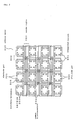
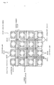
- integrated circuits 201 on silicon wafer 200 are arrayed in a matrix and spaced by scribe regions 202 which serve as dividing lines of given width.
- Each of integrated circuits 201 has four electrode pads 203. These electrode pads 203 serve to apply a power supply voltage and a control signal to integrated circuit 201 for inspecting characteristics of integrated circuit 201.
- Each of scribe regions 202 contains as many common interconnections 204 as the number of electrode pads 203 of each integrated circuit 201, i.e., four common interconnections 204.
- Each integrated circuit 201 has switching transistors 205 and EEPROMs 206 as nonvolatile memories, each paired with one electrode pad 203.
- scribe regions 202 are present also on areas of silicon wafer 200 outside of integrated circuits 201, and contain two common interconnections 204 on each of left and right sides of silicon wafer 200.
- EEPROMs Electrical Erasable Programmable Read Only Memories
- Switching transistors 205 selectively connect and disconnect common interconnections 204 and electrode pads 203 according to on data stored by EEPROMs 206.
- EEPROMs 206 store binary data for selectively turning on and off switching transistors 205.
- circuit forming devices 103 On each of circuit forming devices 103, when integrated circuits 201 are manufactured, switching transistors 205 are turned off according to default binary data stored in EEPROMs 206, disconnecting electrode pads 203 from corresponding common interconnections 204.
- Burn-in tester 104 has probe electrodes and an X/Y stage (not shown), and performs functions of first and second inspection processes for inspecting whether integrated circuits 201 are acceptable or not, a function for selectively connecting and disconnecting electrode pads 203 and common interconnections 204, and a function for applying stresses to integrated circuits 201 under the control of integrated controller 101.
- burn-in tester 104 carries out the first inspection process. Since switching transistors 205 are turned off according to the default settings, burn-in tester 104 successively checks if each of integrated circuits 201 is acceptable or not using electrode pads 203.
- Burn-in tester 104 checks characteristics of integrated circuits 201, and determine whether integrated circuits 201 are acceptable or not based on the checked characteristics thereof.
- Burn-in tester 104 changes the binary data stored in EEPROMs 206 of only those integrated circuits 201 which have been judged as being acceptable in the first inspection process, thereby to turn on switching transistors 205, thus connecting electrode pads 203 to corresponding common interconnections 204.
- Burn-in tester 104 which has thus connected electrode pads 203 to corresponding common interconnections 204 apply uniform stresses to integrated circuits 201 connected to common interconnections 204. Specifically, burn-in tester 104 connect the probe electrodes to respective four electrode pads 203 of either one of integrated circuits 201 connected to common interconnections 204, and apply a rated power supply voltage or higher and a control signal from the probe electrodes to electrode pads 203 for a predetermined period of time. Since the power supply voltage and the control signal are supplied uniformly to all integrated circuits 201 connected by common interconnections 204, all integrated circuits 201 which have been judged as being acceptable in the first inspection process are uniformly stressed.
- Integrated controller 101 acquires data of the results of the first and second inspection processes, and judges, as being defective, those integrated circuits whose characteristics have exhibited profound changes after they have been stressed and those integrated circuits whose characteristics are poor after they have been stressed.
- Dicing device 105 severs silicon wafer 200 introduced by wafer feed mechanism 102 along scribe regions 202 into circuit chips 210 carrying respective integrated circuits 201.
- Chip sorter 106 comprises a robot arm designed for precision works, for example, and sorts out circuit chips 210 introduced by wafer feed mechanism 102 into acceptable ones and defective ones according to the decision made by integrated controller 101 based on the results of the first and second inspection processes carried out by burn-in tester 104.
- a method of manufacturing chips on chip manufacturing system 100 will be described below with reference to Figs. 3 and 4.
- a number of integrated circuits 201 arrayed in a matrix and spaced by scribe regions 202, each of integrated circuits 201 having four electrode pads 203, are formed on the surface of silicon wafer 200 in step 1.
- Switching transistor 205 and EEPROM 206 connected thereto are formed on each integrated circuit 201 in combination with each electrode pad 203. Electrode pads 203 and corresponding common interconnections 204 are connected to each other by switching transistors 205. In an initial stage, default data stored in EEPROMs 206 turn off switching transistors 205, disconnecting electrode pads 203 from common interconnections 204.
- integrated circuits 201 are allocated respective circuit numbers. Integrated circuits 201 are judged as being acceptable or not based on their checked characteristics in step 4, and circuit numbers of those integrated circuits 201 are judged as being acceptable are registered in step 5.
- step 8 the circuit numbers of those integrated circuits 201 are judged as being acceptable are successively read out in step 8, and the binary data stored in EEPROMs 206 of integrated circuits 201 which are represented by the read circuit numbers are changed. Since switching transistors 205 of those integrated circuits 201 are turned on, electrode pads 203 of only acceptable integrated circuits 201 are connected to common interconnections 204 in step 9.
- probe electrodes are connected respectively to four electrode pads 203 of either one of integrated circuits 201 which have been judged as being acceptable, and a rated power supply voltage or higher and a control signal are applied from the probe electrodes to electrode pads 203 for a predetermined period of time, thus stressing integrated circuits 201 in steps 11, 12. Since electrode pads 203 of integrated circuits 201 which have been judged as being acceptable are interconnected by common interconnections, all integrated circuits 201 which have been judged as being acceptable are uniformly stressed.
- step 4 When the application of the stresses is completed, the circuit numbers of those integrated circuits 201 are judged as being acceptable in step 4 are successively read out in steps 13, 15 (see Fig. 4), and the binary data stored in EEPROMs 206 of integrated circuits 201 which are represented by the read circuit numbers are changed, disconnecting electrode pads 203 from common interconnections 204 in step 14.
- circuit chips 210 are sorted out according to the results of the second characteristic inspecting process in steps 22, 23.
- electrode pads 203 are disconnected from common interconnections 204. Therefore, integrated circuits 201 can reliably be inspected.
- acceptable circuit chips 210 can quickly be produced without an unnecessary process of inspecting those integrated circuit 201 which have been judged as being defective in the first inspecting process. For example, even if there is integrated circuit 201 with short-circuited electrode pads 203, the power supply voltage for applying stresses is not applied to such integrated circuit 201, but applied to only those integrated circuits 201 which need to be stressed.
- silicon wafer 200 Many integrated circuits 210 are arrayed on silicon wafer 200 with scribe regions 202 of given width interposed therebetween, and common interconnections 204 are formed in scribe regions 202. Therefore, silicon wafer 200 does not need any dedicated regions for forming common interconnections 204 therein.
- Switching transistors 205 for selectively connecting and disconnecting electrode pads 203 and common interconnections 204 are turned on and off according to the binary data stored in EEPROMs 206. Therefore, the connection between electrode pads 203 and common interconnections 204 can reliably be controlled with a simple structure.
- integrated circuits 201 are arrayed in four rows and four columns on silicon wafer 200, with four electrode pads 203 included in each integrated circuit 201.
- the numbers of integrated circuits 201 and electrode pads 203 may freely be changed.
- modified silicon wafer 300 may have dedicated electrode terminals 301 connected to common interconnections 204, and the probe electrodes may be connected to dedicated electrode terminals 301.
- switching transistors 205 and EEPROMs 206 which are used only in the manufacturing process are formed as part of integrated circuits 201.
- ching transistors 205 and EEPROMs 206 may be formed in scribe regions 202.
- switching transistors 205 are turned off by predetermined default data stored in EEPROMs 206 in the manufacturing stage. However, it is possible to set data for turning off switching transistors 205 in EEPROMs 206 prior to the first inspecting process.
- single burn-in tester 104 performs the functions of the first and second 'inspection processes for inspecting whether integrated circuits 201 are acceptable or not, the function for selectively connecting and disconnecting electrode pads 203 and common interconnections 204, and the function for applying stresses to integrated circuits 201. However, these functions may be performed by respective dedicated devices.
- integrated circuits 201 are inspected before and after they are stressed. However, it is possible to inspect integrated circuits 201 only after they are stressed.
- switching transistors 205 are turned off by default data set in the manufacturing stage. However, it is possible to turn off switching transistors 205 sometime before integrated circuits 201 are inspected irrespective of the manufacturing process.
- the functions of the present invention may be performed in one way or another.
- the functions may be performed by a dedicated piece of hardware for performing given functions, an information processing apparatus which is controlled to perform given functions by a computer program, a predetermined function block provided in an information processing apparatus by a computer program, or a combination thereof.
- the functions of the present invention do not need to be performed by respective independent apparatus.
- a plurality of functions may be performed by a single apparatus, an apparatus for performing a function may be included in an apparatus for performing another function, or part of a function and part of another function may be performed by a single apparatus.
Landscapes
- Engineering & Computer Science (AREA)
- Environmental & Geological Engineering (AREA)
- Computer Hardware Design (AREA)
- Microelectronics & Electronic Packaging (AREA)
- General Engineering & Computer Science (AREA)
- Physics & Mathematics (AREA)
- General Physics & Mathematics (AREA)
- Testing Or Measuring Of Semiconductors Or The Like (AREA)
- Tests Of Electronic Circuits (AREA)
- Testing Of Individual Semiconductor Devices (AREA)
Abstract
Description
Claims (19)
- A method of manufacturing a plurality of chips by dividing a plurality of integrated circuits arrayed on a single circuit substrate, each of the integrated circuits having a plurality of electrode pads, after the integrated circuits are inspected, said method comprising the steps of:forming common interconnections connectable in common to like electrode pads of the integrated circuits, on said circuit substrate;applying uniform stresses from said common interconnections to said integrated circuits while the electrode pads of the integrated circuits are being connected to said common interconnections corresponding thereto;disconnecting said electrode pads from said common interconnections; andindividually inspecting the integrated circuits disconnected from said common interconnections to determine whether the integrated circuits are acceptable or not, using said electrode pads.
- A method according to claim 1, wherein said integrated circuits are arrayed on said circuit substrate with dividing lines of given width interposed therebetween, said common interconnections being formed on said dividing lines.
- A method according to claim 1, further comprising the step of:forming connection control means associated respectively with said electrode pads on said circuit substrate, for selectively connecting and disconnecting the electrode pads and the common interconnections corresponding thereto.
- A method of manufacturing a plurality of chips by dividing a plurality of integrated circuits arrayed on a single circuit substrate, each of the integrated circuits having a plurality of electrode pads, after the integrated circuits are inspected, said method comprising the steps of:forming common interconnections connectable in common to like electrode pads of the integrated circuits, on said circuit substrate;individually inspecting the integrated circuits to determine whether the integrated circuits are acceptable or not, using said electrode pads, while the electrode pads of the integrated circuits are not being connected to said common interconnections corresponding thereto;connecting said electrode pads of the integrated circuits which have been judged as being acceptable to said common interconnections corresponding thereto;applying uniform stresses from said common interconnections to said integrated circuits;disconnecting said electrode pads from said common interconnections; andindividually inspecting again said integrated circuits which have been judged as being acceptable, using said electrode pads.
- A method according to claim 4, wherein said integrated circuits are arrayed on said circuit substrate with dividing lines of given width interposed therebetween, said common interconnections being formed on said dividing lines.
- A method according to claim 4, further comprising the step of:forming connection control means associated respectively with said electrode pads on said circuit substrate, for selectively connecting and disconnecting the electrode pads and the common interconnections corresponding thereto.
- A method according to claim 6, wherein said integrated circuits are arrayed on said circuit substrate with dividing lines of given width interposed therebetween, said common interconnections being formed on said dividing lines.
- A method according to claim 6, wherein said connection control means comprises:switching transistors for selectively connecting and disconnecting the electrode pads and said common interconnections; andEEPROMs for storing binary data for selectively turning on and off said switching transistors.
- A method according to claim 8, wherein said integrated circuits are arrayed on said circuit substrate with dividing lines of given width interposed therebetween, said common interconnections being formed on said dividing lines.
- A system for manufacturing a plurality of chips by dividing a plurality of integrated circuits arrayed on a single circuit substrate, each of the integrated circuits having a plurality of electrode pads, after the integrated circuits are inspected, said method comprising the steps of:circuit forming means for forming common interconnections connectable in common to like electrode pads of the integrated circuits, on said circuit substrate;stress applying means for applying uniform stresses from said common interconnections to said integrated circuits while the electrode pads of the integrated circuits are being connected to said common interconnections corresponding thereto;interconnection disconnecting means for disconnecting said electrode pads from said common interconnections after the stresses have been applied to said integrated circuits by said stress applying means; andcircuit inspecting means for individually inspecting the integrated circuits disconnected from said common interconnections by said interconnection disconnecting means to determine whether the integrated circuits are acceptable or not, using said electrode pads.
- A system for manufacturing a plurality of chips by dividing a plurality of integrated circuits arrayed on a single circuit substrate, each of the integrated circuits having a plurality of electrode pads, after the integrated circuits are inspected, said method comprising the steps of:circuit forming means for forming common interconnections connectable in common to like electrode pads of the integrated circuits, on said circuit substrate;first inspecting means for individually inspecting the integrated circuits to determine whether the integrated circuits are acceptable or not, using said electrode pads, while the electrode pads of the integrated circuits are not being connected to said common interconnections corresponding thereto;interconnection connecting means for connecting said electrode pads of the integrated circuits which have been judged as being acceptable by said first inspecting means to said common interconnections corresponding thereto;stress applying means for applying uniform stresses from said common interconnections to said integrated circuits;interconnection disconnecting means for disconnecting said electrode pads from said common interconnections; andsecond inspecting means for individually inspecting again said integrated circuits which have been judged as being acceptable by said first inspecting means, using said electrode pads.
- A circuit substrate having a plurality of integrated circuits arrayed thereon, each of the integrated circuits having a plurality of electrode pads, comprising:a plurality of common interconnections connectable in common to the electrode pads of the integrated circuits; andconnection control means for selectively connecting and disconnecting the electrode pads and the common interconnections corresponding thereto.
- A circuit substrate according to claim 12, wherein said integrated circuits are arrayed on said circuit substrate with dividing lines of given width interposed therebetween, said common interconnections being formed on said dividing lines.
- A circuit substrate according to claim 12, wherein said connection control means comprises:switching transistors for selectively connecting and disconnecting the electrode pads and said common interconnections; andEEPROMs for storing binary data for selectively turning on and off said switching transistors.
- A circuit substrate according to claim 14, wherein said integrated circuits are arrayed on said circuit substrate with dividing lines of given width interposed therebetween, said common interconnections being formed on said dividing lines.
- A method of inspecting integrated circuits on a circuit substrate according to claim 12, comprising the steps of:applying uniform stresses from said common interconnections to said integrated circuits while the electrode pads of the integrated circuits are being connected to said common interconnections corresponding thereto;disconnecting said electrode pads from said common interconnections; andindividually inspecting the integrated circuits disconnected from said common interconnections to determine whether the integrated circuits are acceptable or not, using said electrode pads.
- A method of inspecting integrated circuits on a circuit substrate according to claim 12, comprising the steps of:individually inspecting the integrated circuits to determine whether the integrated circuits are acceptable or not, using said electrode pads, while the electrode pads of the integrated circuits are not being connected to said common interconnections corresponding thereto;connecting said electrode pads of the integrated circuits which have been judged as being acceptable to said common interconnections corresponding thereto;applying uniform stresses from said common interconnections to said integrated circuits;disconnecting said electrode pads from said common interconnections; andindividually inspecting said integrated circuits which have been judged as being acceptable, using said electrode pads.
- A system for inspecting integrated circuits on a circuit substrate according to claim 12, comprising:stress applying means for applying uniform stresses from said common interconnections to said integrated circuits while the electrode pads of the integrated circuits are being connected to said common interconnections corresponding thereto;interconnection disconnecting means for disconnecting said electrode pads from said common interconnections after the stresses have been applied to said integrated circuits by said stress applying means; andcircuit inspecting means for individually inspecting the integrated circuits disconnected from said common interconnections by said interconnection disconnecting means to determine whether the integrated circuits are acceptable or not, using said electrode pads.
- A system for inspecting integrated circuits on a circuit substrate according to claim 12, comprising:first inspecting means for individually inspecting the integrated circuits to determine whether the integrated circuits are acceptable or not, using said electrode pads, while the electrode pads of the integrated circuits are not being connected to said common interconnections corresponding thereto;interconnection connecting means for connecting said electrode pads of the integrated circuits which have been judged as being acceptable by said first inspecting means to said common interconnections corresponding thereto;stress applying means for applying uniform stresses from said common interconnections to said integrated circuits;interconnection disconnecting means for disconnecting said electrode pads from said common interconnections; andsecond inspecting means for individually inspecting again said integrated circuits which have been judged as being acceptable by said first inspecting means, using said electrode pads.
Applications Claiming Priority (2)
| Application Number | Priority Date | Filing Date | Title |
|---|---|---|---|
| JP2002004504 | 2002-01-11 | ||
| JP2002004504A JP2003209147A (en) | 2002-01-11 | 2002-01-11 | Chip manufacturing method and system |
Publications (2)
| Publication Number | Publication Date |
|---|---|
| EP1328016A2 true EP1328016A2 (en) | 2003-07-16 |
| EP1328016A3 EP1328016A3 (en) | 2004-02-04 |
Family
ID=19191012
Family Applications (1)
| Application Number | Title | Priority Date | Filing Date |
|---|---|---|---|
| EP03000272A Withdrawn EP1328016A3 (en) | 2002-01-11 | 2003-01-08 | Wafer-level test of integrated circuits |
Country Status (3)
| Country | Link |
|---|---|
| US (1) | US6900655B2 (en) |
| EP (1) | EP1328016A3 (en) |
| JP (1) | JP2003209147A (en) |
Families Citing this family (4)
| Publication number | Priority date | Publication date | Assignee | Title |
|---|---|---|---|---|
| JP4464237B2 (en) * | 2004-09-30 | 2010-05-19 | Necエレクトロニクス株式会社 | Burn-in test method and burn-in measurement program used therefor |
| US8436636B2 (en) * | 2006-10-10 | 2013-05-07 | Apple Inc. | Methods and apparatuses for testing circuit boards |
| US8362793B2 (en) * | 2006-11-07 | 2013-01-29 | Apple Inc. | Circuit boards including removable test point portions and configurable testing platforms |
| US8081003B2 (en) * | 2009-02-02 | 2011-12-20 | Infineon Technologies Ag | Circuit arrangement with a test circuit and a reference circuit and corresponding method |
Family Cites Families (9)
| Publication number | Priority date | Publication date | Assignee | Title |
|---|---|---|---|---|
| JPS63217821A (en) | 1987-03-06 | 1988-09-09 | Toshiba Corp | Semiconductor integrated circuit |
| US5315241A (en) | 1991-09-18 | 1994-05-24 | Sgs-Thomson Microelectronics, Inc. | Method for testing integrated circuits |
| JP2918397B2 (en) | 1992-06-26 | 1999-07-12 | 三菱電機株式会社 | Semiconductor wafer and method of manufacturing the same |
| JPH06230086A (en) | 1992-09-22 | 1994-08-19 | Nec Corp | Lsi testing circuit |
| JPH07169807A (en) * | 1993-12-16 | 1995-07-04 | Nippondenso Co Ltd | Semiconductor wafer |
| US5619462A (en) * | 1995-07-31 | 1997-04-08 | Sgs-Thomson Microelectronics, Inc. | Fault detection for entire wafer stress test |
| GB2307783B (en) * | 1995-09-30 | 2000-04-05 | Motorola Ltd | Enhanced security semiconductor device, semiconductor circuit arrangement, and method of production thereof |
| US6046600A (en) | 1995-10-31 | 2000-04-04 | Texas Instruments Incorporated | Process of testing integrated circuit dies on a wafer |
| JPH11330176A (en) | 1998-05-19 | 1999-11-30 | Fujitsu Ltd | Semiconductor integrated circuit device |
-
2002
- 2002-01-11 JP JP2002004504A patent/JP2003209147A/en active Pending
- 2002-12-24 US US10/327,037 patent/US6900655B2/en not_active Expired - Fee Related
-
2003
- 2003-01-08 EP EP03000272A patent/EP1328016A3/en not_active Withdrawn
Also Published As
| Publication number | Publication date |
|---|---|
| US6900655B2 (en) | 2005-05-31 |
| US20030132489A1 (en) | 2003-07-17 |
| JP2003209147A (en) | 2003-07-25 |
| EP1328016A3 (en) | 2004-02-04 |
Similar Documents
| Publication | Publication Date | Title |
|---|---|---|
| US6288561B1 (en) | Method and apparatus for probing, testing, burn-in, repairing and programming of integrated circuits in a closed environment using a single apparatus | |
| US6630685B1 (en) | Probe look ahead: testing parts not currently under a probehead | |
| US6871307B2 (en) | Efficient test structure for non-volatile memory and other semiconductor integrated circuits | |
| US7555358B2 (en) | Process and method for continuous, non lot-based integrated circuit manufacturing | |
| CN114152858A (en) | Electrical test device and test method for cutting channel device | |
| US20020070746A1 (en) | Method and apparatus for testing semiconductor devices | |
| US6963213B1 (en) | Auto-recovery wafer testing apparatus and wafer testing method | |
| US20080004829A1 (en) | Method and apparatus for automatic test equipment | |
| US6900655B2 (en) | Determination of whether integrated circuit is acceptable or not in wafer-level burn-in test | |
| KR100821095B1 (en) | Semiconductor test apparatus and test method | |
| US20030045010A1 (en) | Method and structure for temporarily isolating a die from a common conductor to facilitate wafer level testing | |
| US6590408B1 (en) | Microelectronic fabrication electrical test apparatus and method providing enhanced electrical test accuracy | |
| US6337576B1 (en) | Wafer-level burn-in | |
| JP2000124278A (en) | Semiconductor device and testing thereof | |
| JPH02136760A (en) | Method for sorting semiconductor element | |
| KR100525103B1 (en) | Wafer business SBL method | |
| KR100641471B1 (en) | Common input ic | |
| JP2002124551A (en) | Semiconductor sorting equipment and method | |
| JPS62179755A (en) | Semiconductor integrated circuit with built-in test circuit | |
| JPH03142852A (en) | Manufacture of wafer scale semiconductor device | |
| JPH04288849A (en) | Wafer structure and burn-in method | |
| JP2001144152A (en) | Manufacturing method of wafer and semiconductor device | |
| JPH02162748A (en) | Manufacture of semiconductor device | |
| JPS63265434A (en) | Probe apparatus | |
| JPH0541426A (en) | Wafer prober for EPROM and wafer prober for redundancy of memory chips |
Legal Events
| Date | Code | Title | Description |
|---|---|---|---|
| PUAI | Public reference made under article 153(3) epc to a published international application that has entered the european phase |
Free format text: ORIGINAL CODE: 0009012 |
|
| AK | Designated contracting states |
Designated state(s): AT BE BG CH CY CZ DE DK EE ES FI FR GB GR HU IE IT LI LU MC NL PT SE SI SK TR |
|
| AX | Request for extension of the european patent |
Extension state: AL LT LV MK RO |
|
| PUAL | Search report despatched |
Free format text: ORIGINAL CODE: 0009013 |
|
| AK | Designated contracting states |
Kind code of ref document: A3 Designated state(s): AT BE BG CH CY CZ DE DK EE ES FI FR GB GR HU IE IT LI LU MC NL PT SE SI SK TR |
|
| AX | Request for extension of the european patent |
Extension state: AL LT LV MK RO |
|
| RIC1 | Information provided on ipc code assigned before grant |
Ipc: 7G 01R 31/316 B Ipc: 7G 01R 31/3185 B Ipc: 7H 01L 21/66 A |
|
| 17P | Request for examination filed |
Effective date: 20040107 |
|
| 17Q | First examination report despatched |
Effective date: 20040817 |
|
| AKX | Designation fees paid |
Designated state(s): DE FR GB |
|
| STAA | Information on the status of an ep patent application or granted ep patent |
Free format text: STATUS: THE APPLICATION HAS BEEN WITHDRAWN |
|
| 18W | Application withdrawn |
Effective date: 20050304 |