EP1327967A2 - Supply current regulator for two-wire sensors - Google Patents
Supply current regulator for two-wire sensors Download PDFInfo
- Publication number
- EP1327967A2 EP1327967A2 EP03007947A EP03007947A EP1327967A2 EP 1327967 A2 EP1327967 A2 EP 1327967A2 EP 03007947 A EP03007947 A EP 03007947A EP 03007947 A EP03007947 A EP 03007947A EP 1327967 A2 EP1327967 A2 EP 1327967A2
- Authority
- EP
- European Patent Office
- Prior art keywords
- current
- resistance
- sensor
- coupled
- output
- Prior art date
- Legal status (The legal status is an assumption and is not a legal conclusion. Google has not performed a legal analysis and makes no representation as to the accuracy of the status listed.)
- Withdrawn
Links
- 239000004020 conductor Substances 0.000 claims abstract description 22
- 230000035945 sensitivity Effects 0.000 description 7
- 230000004048 modification Effects 0.000 description 3
- 238000012986 modification Methods 0.000 description 3
- 238000010586 diagram Methods 0.000 description 2
- 230000001105 regulatory effect Effects 0.000 description 2
- 230000004907 flux Effects 0.000 description 1
- 239000000463 material Substances 0.000 description 1
- 229910000889 permalloy Inorganic materials 0.000 description 1
- 230000004044 response Effects 0.000 description 1
- 229920006395 saturated elastomer Polymers 0.000 description 1
Images

Classifications
-
- G—PHYSICS
- G08—SIGNALLING
- G08C—TRANSMISSION SYSTEMS FOR MEASURED VALUES, CONTROL OR SIMILAR SIGNALS
- G08C19/00—Electric signal transmission systems
- G08C19/02—Electric signal transmission systems in which the signal transmitted is magnitude of current or voltage
-
- G—PHYSICS
- G05—CONTROLLING; REGULATING
- G05F—SYSTEMS FOR REGULATING ELECTRIC OR MAGNETIC VARIABLES
- G05F1/00—Automatic systems in which deviations of an electric quantity from one or more predetermined values are detected at the output of the system and fed back to a device within the system to restore the detected quantity to its predetermined value or values, i.e. retroactive systems
- G05F1/10—Regulating voltage or current
- G05F1/46—Regulating voltage or current wherein the variable actually regulated by the final control device is DC
- G05F1/56—Regulating voltage or current wherein the variable actually regulated by the final control device is DC using semiconductor devices in series with the load as final control devices
- G05F1/565—Regulating voltage or current wherein the variable actually regulated by the final control device is DC using semiconductor devices in series with the load as final control devices sensing a condition of the system or its load in addition to means responsive to deviations in the output of the system, e.g. current, voltage, power factor
Definitions
- the present invention relates generally to supply current regulators for two wire sensors.
- a two wire sensor is commonly used to sense a condition and to transmit a measure of the sensed condition over two wires to a controller or indicator.
- the two wire sensor is typically supplied with a voltage V S over two wires, and the two wire sensor controls the supply current I S in response to the sensed condition.
- This supply current I S is detected by a controller in order to control a load, and/or the supply current I S is detected by an indicator in order to give an indication of the condition being sensed.
- a transducer and its associated circuitry of a two wire sensor are referred to herein as a sensor load.
- the present invention is directed to an arrangement which solves one or more of the problems of prior art two wire sensor current sources.
- a current regulator for a two wire sensor comprises first and second conductors, a first resistance, a second resistance, and an amplifier.
- the first and second conductors are arranged to provide a sensor output current.
- the first resistance and a current reference are coupled across the first and second conductors.
- the second resistance and sensor load terminals are coupled across the first and second conductors.
- the amplifier has first and second inputs and an output. The first input is coupled to a first junction between the first resistance and the current reference, the second input is coupled to a second junction between the second resistance and the sensor load terminals, and the output is connected so as to control the sensor output current in the first and second conductors.
- the amplifier is arranged so that a first voltage at the first junction is substantially equal to a second voltage at the second junction.
- a two wire sensor 10 typically comprises a pair of conductors 12 and 14 connected to a sensor/regulator 16.
- a voltage V S is provided across the conductors 12 and 14, and the sensor/regulator 16 controls a supply current I S in accordance with a condition being sensed.
- the supply current I S therefore, is detected from the conductors 12 and 14 and is used by a controller to control the sensed condition and/or by an indicator to indicate the sensed condition.
- a two wire sensor 20 in accordance with the present invention is shown in Figure 2.
- the two wire sensor 20 includes a pair of conductors 22 and 24.
- a voltage V S is provided across the conductors 22 and 24.
- Also connected across the conductors 22 and 24 are a first resistance 26 and a current reference 28 having a junction 30 therebetween.
- the current reference 28 provides a current I REF such that the current I 1 through the first resistance 26 and the current I REF are substantially related according to the following equation:
- I sub 1 ⁇ ⁇ I sub ⁇ REF ⁇
- a second resistance 32 and a sensor load 34 are connected across the conductors 22 and 24 and form a junction 36 therebetween.
- the sensor load 34 includes a transducer that transduces the desired condition.
- An operational transconductance amplifier 38 (OTA) has a first input connected to the junction 30, a second input connected to the junction 36, and an output also connected to the junction 36.
- V OS is small and is the input offset voltage of the operational transconductance amplifier 38.
- the negative feedback and high gain of the operational transconductance amplifier 38 forces the voltage V 2 to be substantially equal to the voltage V 1 .
- the supply current I S is substantially a function of only the current I REF and the ratio of R 1 to R 2 , if it is assumed that the offset voltage V OS and the quiescent current I Q are minimized.
- the quiescent current I Q can be minimized, for example, by biasing the operational transconductance amplifier 38 at the voltage V 2 instead of at the supply voltage V S as shown in Figure 2.
- the current reference 28 is constructed to be substantially insensitive to fluctuations of the supply voltage V S and of temperature.
- the ratio of R 1 to R 2 is used only as a scaling factor. Accordingly, the current reference 28 provides the desired encoding of the supply current I S so as to indicate only the condition being sensed.
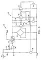
- the sensor load 34 includes a bandgap voltage regulator 50 which provides a regulated voltage to the remainder of the sensor load 34 and to the current reference 28.
- a transducer 52 is connected to the output of the voltage regulator 50, and converts the sensed condition into an electrical signal that is a measure of the sensed condition and that is supplied to an input of a resistively loaded differential amplifier 54.
- the transducer 52 may be a wheatstone bridge which is comprised of resistors fabricated with Permalloy and which converts a differential magnetic flux density into an electrical signal that is fed to the differential amplifier 54.
- This type of transducer in conjunction with a ring magnet, is particularly useful in sensing the speed of rotation of a rotating device such as a wheel. As the ring magnet rotates, its rotating pole pieces produce output pulses from the wheatstone bridge that alternately switch the outputs of the differential amplifier 54 between high and low states.
- the transducer 52 may be arranged otherwise in order to sense rotation or any other condition.
- the differential amplifier 54 together with a comparator 56 and a hysteresis generator 58, form a threshold switch 60.
- the hysteresis generator 58 is a saturated differential amplifier having collectors which pull the bias current I DIFF through one or the other of the load resistors R L of the differential amplifier 54, thus creating an offset voltage which the output of the transducer 52 must overcome before the comparator 56 can switch.
- the hysteresis generator 58 saturates in the opposite condition creating a hysteresis (i.e., a differential) which the transducer 52 must overcome before the comparator 56 can again switch.
- the outputs of the comparator 56 are connected to a differential-to-single-ended amplifier 62 which drives the base of a transistor switch 64.
- the threshold switch 60 switches between its two output states, the base of the transistor switch 64 is operated by the amplifier 62 between a shorted state, in which the base and emitter of the transistor switch 64 are essentially shorted together, and an over driven state.
- the collector of the transistor switch 64 is a high impedance and the transistor switch 64 is open.
- the over driven state the collector of the transistor switch 64 is driven into low impedance saturation and the transistor switch 64 is closed.
- the transistor switch 64 modifies the current I REF provided by the current reference 28 so as to encode the supply current I S between two levels.
- the current reference 28 includes transistors 70 and 72 and resistances 74 and 76.
- the transistor 70 has its collector connected to the junction 30, its emitter connected to the transistor 72, and its base connected to the voltage regulator 50 to receive a bias voltage V BIAS .
- the collector and base of the transistor 72 are tied together so that the transistor 72 functions as a diode.
- the resistance 74 is connected between the emitter of the transistor 72 and the conductor 24, and the resistance 76 is connected between the emitter of the transistor 72 and the collector of the transistor switch 64.
- the circuit of the resistance 76 is opened and closed.
- the resistances 74 and 76 are in parallel such that their combined value is lower than the value of the resistance 74 alone. Therefore, the current I REF assumes its high state. Consequently, the supply current I S assumes its high state.
- the resistance 76 is disconnected from the resistance 74 such that their combined value becomes the value of the resistance 74. Therefore, the current I REF assumes its low state. Consequently, the supply current I S assumes its low state.
- the transistor 70 is controlled by the voltage regulator 50, the sensitivity of the voltage across the resistances 74 and 76 to fluctuations of the supply voltage V S is minimized.
- the sensitivity of the reference current I REF to fluctuations of temperature is minimized by proper selection of the components of the current reference 28.
- the sensitivity of the voltage at the emitter of the transistor 72 to temperature must equal the sensitivity of the resistances 74 and 76 to temperature.
- This equalization can be achieved by forming the resistances 74 and 76 from a material with a temperature coefficient of resistance (TCR) that is nearly proportional to absolute temperature (PTAT) and by choosing the voltage level of V BIAS which results in the voltage at the emitter of the transistor 72 being PTAT.
- TCR temperature coefficient of resistance
- I REF will be substantially insensitive to temperature fluctuations.
- the threshold switch 60 drives the supply current I S between two levels as a function of the output of the transducer 52.
- the supply current I S can be driven to any number of discrete states, or the supply current I S can be controlled so that it is smoothly varying.
- a smoothly varying current is equivalent to a current having a very large number of discrete steps.
Landscapes
- Engineering & Computer Science (AREA)
- General Physics & Mathematics (AREA)
- Physics & Mathematics (AREA)
- Electromagnetism (AREA)
- Radar, Positioning & Navigation (AREA)
- Automation & Control Theory (AREA)
- Continuous-Control Power Sources That Use Transistors (AREA)
- Measurement Of Current Or Voltage (AREA)
- Arrangements For Transmission Of Measured Signals (AREA)
- Measuring Instrument Details And Bridges, And Automatic Balancing Devices (AREA)
- Interface Circuits In Exchanges (AREA)
- Testing Of Short-Circuits, Discontinuities, Leakage, Or Incorrect Line Connections (AREA)
- Measuring Pulse, Heart Rate, Blood Pressure Or Blood Flow (AREA)
- Selective Calling Equipment (AREA)
Abstract
Description
Claims (8)
- A current regulator for a two wire sensor comprising:first and second conductors are arranged to provide a sensor output current;a first resistance and a current reference coupled across the first and second conductors;a second resistance and sensor load terminals coupled across the first and second conductors; and,an amplifier having first and second inputs and an output, wherein the first input is coupled to a first junction between the first resistance and the current reference, wherein the second input is coupled to a second junction between the second resistance and the sensor load terminals, wherein the output is connected so as to control the sensor output current in the first and second conductors, and wherein the amplifier is arranged so that a first voltage at the first junction is substantially equal to a second voltage at the second junction.
- The current regulator of claim 1, wherein a sensor load is coupled to the sensor load terminals, and wherein the sensor load is coupled to the current reference so as to control the sensor output current.
- The current regulator of claim 2, wherein the current reference includes a variable resistance coupled between the first junction and one of the first and second conductors, and wherein the variable resistance is coupled to the sensor load so as to control the sensor output current.
- The current regulator of claim 3, wherein the output is coupled to the second input.
- The current regulator of claim 3, wherein the sensor load includes a switch arranged to switch the variable resistance between only two discrete resistances.
- The current regulator of claim 3, wherein the sensor load includes a switch arranged to switch the variable resistance between a plurality of discrete resistances.
- The current regulator of claim 1 or 3, wherein the amplifier is an operational amplifier.
- The current regulator of claim 1 or 7, wherein the output is coupled to the second input.
Applications Claiming Priority (3)
| Application Number | Priority Date | Filing Date | Title |
|---|---|---|---|
| US09/429,445 US6118260A (en) | 1999-10-28 | 1999-10-28 | Supply current regulator for two-wire sensors |
| US429445 | 1999-10-28 | ||
| EP00973649A EP1254444B1 (en) | 1999-10-28 | 2000-10-19 | Supply current regulator for two-wire sensors |
Related Parent Applications (1)
| Application Number | Title | Priority Date | Filing Date |
|---|---|---|---|
| EP00973649A Division EP1254444B1 (en) | 1999-10-28 | 2000-10-19 | Supply current regulator for two-wire sensors |
Publications (2)
| Publication Number | Publication Date |
|---|---|
| EP1327967A2 true EP1327967A2 (en) | 2003-07-16 |
| EP1327967A3 EP1327967A3 (en) | 2004-12-08 |
Family
ID=23703281
Family Applications (2)
| Application Number | Title | Priority Date | Filing Date |
|---|---|---|---|
| EP00973649A Expired - Lifetime EP1254444B1 (en) | 1999-10-28 | 2000-10-19 | Supply current regulator for two-wire sensors |
| EP03007947A Withdrawn EP1327967A3 (en) | 1999-10-28 | 2000-10-19 | Supply current regulator for two-wire sensors |
Family Applications Before (1)
| Application Number | Title | Priority Date | Filing Date |
|---|---|---|---|
| EP00973649A Expired - Lifetime EP1254444B1 (en) | 1999-10-28 | 2000-10-19 | Supply current regulator for two-wire sensors |
Country Status (18)
| Country | Link |
|---|---|
| US (1) | US6118260A (en) |
| EP (2) | EP1254444B1 (en) |
| JP (1) | JP2003513382A (en) |
| KR (1) | KR20020048985A (en) |
| AT (1) | ATE267433T1 (en) |
| AU (1) | AU769844B2 (en) |
| BR (1) | BR0015074A (en) |
| CA (1) | CA2389073A1 (en) |
| CZ (1) | CZ20021488A3 (en) |
| DE (1) | DE60010935T2 (en) |
| HU (1) | HUP0203687A2 (en) |
| IL (1) | IL149354A0 (en) |
| MX (1) | MXPA02004100A (en) |
| NO (1) | NO20021966L (en) |
| NZ (1) | NZ519205A (en) |
| PL (1) | PL355013A1 (en) |
| TR (1) | TR200201170T2 (en) |
| WO (1) | WO2001031606A1 (en) |
Families Citing this family (9)
| Publication number | Priority date | Publication date | Assignee | Title |
|---|---|---|---|---|
| DE10145520B4 (en) * | 2001-09-14 | 2004-09-09 | Vega Grieshaber Kg | Circuit arrangement for the voltage supply of a two-wire sensor |
| DE10146204A1 (en) * | 2001-09-19 | 2003-04-10 | Grieshaber Vega Kg | Circuit arrangement for the voltage supply of a two-wire sensor |
| GB0227461D0 (en) * | 2002-11-25 | 2002-12-31 | Goodrich Control Sys Ltd | A method of and apparatus for detecting sensor loss in a generator control system |
| JP2006109349A (en) * | 2004-10-08 | 2006-04-20 | Ricoh Co Ltd | Constant current circuit and system power supply device using the constant current circuit |
| US7719411B2 (en) * | 2007-06-12 | 2010-05-18 | Robert Bosch Gmbh | Method and system of transmitting a plurality of movement parameters of a vehicle via a two-wire interface |
| DE102007036580A1 (en) | 2007-08-02 | 2009-02-05 | Endress + Hauser Flowtec Ag | Fieldbus unit for a two-wire fieldbus |
| US8054071B2 (en) | 2008-03-06 | 2011-11-08 | Allegro Microsystems, Inc. | Two-terminal linear sensor |
| DE102008041030A1 (en) * | 2008-08-06 | 2010-02-11 | Robert Bosch Gmbh | Device and method for detecting a measured variable |
| DE102022129856A1 (en) * | 2022-11-11 | 2024-05-16 | Vega Grieshaber Kg | Implementation of a voltage without direct measurement reference |
Family Cites Families (5)
| Publication number | Priority date | Publication date | Assignee | Title |
|---|---|---|---|---|
| US4446417A (en) * | 1982-02-12 | 1984-05-01 | Westinghouse Electric Corp. | Voltage regulator for aircraft generators |
| US5616846A (en) * | 1994-10-27 | 1997-04-01 | Kwasnik; Joseph W. | Method and apparatus for current regulation and temperature compensation |
| US5959372A (en) * | 1997-07-21 | 1999-09-28 | Emerson Electric Co. | Power management circuit |
| DE19756233A1 (en) * | 1997-12-17 | 1999-07-01 | Siemens Ag | Current-voltage regulator |
| US5917312A (en) * | 1998-06-16 | 1999-06-29 | Lucent Technologies Inc. | System and method for voltage positioning a regulator and regulator employing the same |
-
1999
- 1999-10-28 US US09/429,445 patent/US6118260A/en not_active Expired - Lifetime
-
2000
- 2000-10-19 TR TR2002/01170T patent/TR200201170T2/en unknown
- 2000-10-19 JP JP2001534113A patent/JP2003513382A/en not_active Withdrawn
- 2000-10-19 BR BR0015074-6A patent/BR0015074A/en not_active Application Discontinuation
- 2000-10-19 NZ NZ519205A patent/NZ519205A/en unknown
- 2000-10-19 EP EP00973649A patent/EP1254444B1/en not_active Expired - Lifetime
- 2000-10-19 IL IL14935400A patent/IL149354A0/en unknown
- 2000-10-19 EP EP03007947A patent/EP1327967A3/en not_active Withdrawn
- 2000-10-19 HU HU0203687A patent/HUP0203687A2/en unknown
- 2000-10-19 MX MXPA02004100A patent/MXPA02004100A/en not_active Application Discontinuation
- 2000-10-19 KR KR1020027005364A patent/KR20020048985A/en not_active Withdrawn
- 2000-10-19 CA CA002389073A patent/CA2389073A1/en not_active Abandoned
- 2000-10-19 AU AU12142/01A patent/AU769844B2/en not_active Ceased
- 2000-10-19 DE DE60010935T patent/DE60010935T2/en not_active Expired - Lifetime
- 2000-10-19 WO PCT/US2000/028840 patent/WO2001031606A1/en not_active Ceased
- 2000-10-19 PL PL00355013A patent/PL355013A1/en unknown
- 2000-10-19 AT AT00973649T patent/ATE267433T1/en not_active IP Right Cessation
- 2000-10-19 CZ CZ20021488A patent/CZ20021488A3/en unknown
-
2002
- 2002-04-25 NO NO20021966A patent/NO20021966L/en not_active Application Discontinuation
Also Published As
| Publication number | Publication date |
|---|---|
| WO2001031606A1 (en) | 2001-05-03 |
| US6118260A (en) | 2000-09-12 |
| AU769844B2 (en) | 2004-02-05 |
| JP2003513382A (en) | 2003-04-08 |
| BR0015074A (en) | 2003-02-25 |
| NO20021966L (en) | 2002-06-12 |
| IL149354A0 (en) | 2002-11-10 |
| NZ519205A (en) | 2003-07-25 |
| NO20021966D0 (en) | 2002-04-25 |
| EP1254444B1 (en) | 2004-05-19 |
| CZ20021488A3 (en) | 2003-03-12 |
| PL355013A1 (en) | 2004-03-22 |
| AU1214201A (en) | 2001-05-08 |
| MXPA02004100A (en) | 2003-08-20 |
| DE60010935T2 (en) | 2005-08-18 |
| TR200201170T2 (en) | 2002-09-23 |
| ATE267433T1 (en) | 2004-06-15 |
| HUP0203687A2 (en) | 2003-02-28 |
| KR20020048985A (en) | 2002-06-24 |
| EP1327967A3 (en) | 2004-12-08 |
| EP1254444A1 (en) | 2002-11-06 |
| DE60010935D1 (en) | 2004-06-24 |
| CA2389073A1 (en) | 2001-05-03 |
Similar Documents
| Publication | Publication Date | Title |
|---|---|---|
| CA1135529A (en) | Semiconductor pressure detector apparatus with zero-point temperature compensation | |
| KR101243473B1 (en) | Voltage divider circuit and magnetic sensor circuit | |
| CA1048622A (en) | Transistor pair temperature sensor | |
| US4639665A (en) | Sensing system for measuring a parameter | |
| JPH0621799B2 (en) | Magnetoresistive differential sensor device | |
| EP1254444B1 (en) | Supply current regulator for two-wire sensors | |
| EP0382217A2 (en) | Power source circuit and bridge type measuring device with output compensating circuit utilizing the same | |
| US4112356A (en) | Semiconductor gas detector circuit | |
| JP4438222B2 (en) | Physical quantity detection device | |
| Pradhan et al. | An improved lead compensation technique for three-wire resistance temperature detectors | |
| US4025847A (en) | Measurement system including bridge circuit | |
| US6918299B2 (en) | Method and apparatus for improving performance of a force balance accelerometer based on a single-coil velocity geophone | |
| JP2001108480A (en) | Sensor threshold circuit | |
| NZ525537A (en) | Supply current regulator for two-wire sensors | |
| EP0423284B1 (en) | Electronic circuit arrangement | |
| JP2015215316A (en) | Hall element drive circuit | |
| JP3230230B2 (en) | Detector | |
| US3105155A (en) | Magnetic comparator | |
| JPS6111779Y2 (en) | ||
| JPH05273320A (en) | Magnetic sensor | |
| SU1649453A1 (en) | Device for measuring the rate and temperature of nonisothermic flow | |
| JPH0824201B2 (en) | Magnetic semiconductor element temperature compensation circuit | |
| JP2003149273A (en) | Current detector | |
| JPS6126120B2 (en) | ||
| JPH0232584B2 (en) | CHOKURYUKADENRYUKENSHUTSUSOCHI |
Legal Events
| Date | Code | Title | Description |
|---|---|---|---|
| PUAI | Public reference made under article 153(3) epc to a published international application that has entered the european phase |
Free format text: ORIGINAL CODE: 0009012 |
|
| 17P | Request for examination filed |
Effective date: 20030423 |
|
| AC | Divisional application: reference to earlier application |
Ref document number: 1254444 Country of ref document: EP Kind code of ref document: P |
|
| AK | Designated contracting states |
Designated state(s): AT BE CH CY DE DK ES FI FR GB GR IE IT LI LU MC NL PT SE |
|
| PUAL | Search report despatched |
Free format text: ORIGINAL CODE: 0009013 |
|
| AK | Designated contracting states |
Kind code of ref document: A3 Designated state(s): AT BE CH CY DE DK ES FI FR GB GR IE IT LI LU MC NL PT SE |
|
| AKX | Designation fees paid |
Designated state(s): AT BE CH CY DE DK ES FI FR GB GR IE IT LI LU MC NL PT SE |
|
| STAA | Information on the status of an ep patent application or granted ep patent |
Free format text: STATUS: THE APPLICATION IS DEEMED TO BE WITHDRAWN |
|
| 18D | Application deemed to be withdrawn |
Effective date: 20050609 |