EP1326269A1 - Method of producing silicon wafer and silicon wafer - Google Patents
Method of producing silicon wafer and silicon wafer Download PDFInfo
- Publication number
- EP1326269A1 EP1326269A1 EP01965658A EP01965658A EP1326269A1 EP 1326269 A1 EP1326269 A1 EP 1326269A1 EP 01965658 A EP01965658 A EP 01965658A EP 01965658 A EP01965658 A EP 01965658A EP 1326269 A1 EP1326269 A1 EP 1326269A1
- Authority
- EP
- European Patent Office
- Prior art keywords
- wafer
- heat treatment
- oxygen concentration
- resistivity
- silicon
- Prior art date
- Legal status (The legal status is an assumption and is not a legal conclusion. Google has not performed a legal analysis and makes no representation as to the accuracy of the status listed.)
- Ceased
Links
Images

Classifications
-
- C—CHEMISTRY; METALLURGY
- C30—CRYSTAL GROWTH
- C30B—SINGLE-CRYSTAL GROWTH; UNIDIRECTIONAL SOLIDIFICATION OF EUTECTIC MATERIAL OR UNIDIRECTIONAL DEMIXING OF EUTECTOID MATERIAL; REFINING BY ZONE-MELTING OF MATERIAL; PRODUCTION OF A HOMOGENEOUS POLYCRYSTALLINE MATERIAL WITH DEFINED STRUCTURE; SINGLE CRYSTALS OR HOMOGENEOUS POLYCRYSTALLINE MATERIAL WITH DEFINED STRUCTURE; AFTER-TREATMENT OF SINGLE CRYSTALS OR A HOMOGENEOUS POLYCRYSTALLINE MATERIAL WITH DEFINED STRUCTURE; APPARATUS THEREFOR
- C30B29/00—Single crystals or homogeneous polycrystalline material with defined structure characterised by the material or by their shape
- C30B29/02—Elements
- C30B29/06—Silicon
-
- H—ELECTRICITY
- H10—SEMICONDUCTOR DEVICES; ELECTRIC SOLID-STATE DEVICES NOT OTHERWISE PROVIDED FOR
- H10P—GENERIC PROCESSES OR APPARATUS FOR THE MANUFACTURE OR TREATMENT OF DEVICES COVERED BY CLASS H10
- H10P36/00—Gettering within semiconductor bodies
-
- C—CHEMISTRY; METALLURGY
- C30—CRYSTAL GROWTH
- C30B—SINGLE-CRYSTAL GROWTH; UNIDIRECTIONAL SOLIDIFICATION OF EUTECTIC MATERIAL OR UNIDIRECTIONAL DEMIXING OF EUTECTOID MATERIAL; REFINING BY ZONE-MELTING OF MATERIAL; PRODUCTION OF A HOMOGENEOUS POLYCRYSTALLINE MATERIAL WITH DEFINED STRUCTURE; SINGLE CRYSTALS OR HOMOGENEOUS POLYCRYSTALLINE MATERIAL WITH DEFINED STRUCTURE; AFTER-TREATMENT OF SINGLE CRYSTALS OR A HOMOGENEOUS POLYCRYSTALLINE MATERIAL WITH DEFINED STRUCTURE; APPARATUS THEREFOR
- C30B33/00—After-treatment of single crystals or homogeneous polycrystalline material with defined structure
-
- H—ELECTRICITY
- H10—SEMICONDUCTOR DEVICES; ELECTRIC SOLID-STATE DEVICES NOT OTHERWISE PROVIDED FOR
- H10P—GENERIC PROCESSES OR APPARATUS FOR THE MANUFACTURE OR TREATMENT OF DEVICES COVERED BY CLASS H10
- H10P36/00—Gettering within semiconductor bodies
- H10P36/20—Intrinsic gettering, i.e. thermally inducing defects by using oxygen present in the silicon body
Definitions
- the present invention relates to a technique by which a DZ-IG silicon wafer having high resistivity and also having high gettering ability can surely be obtained.
- Silicon wafers of high resistivity produced by the floating zone method have conventionally been used for power devices such as high-voltage power devices and thyristors.
- FZ method floating zone method
- it is difficult to produce a silicon wafer having a large diameter of 200 mm or more by the FZ method and the radial resistivity distribution of usual FZ wafers is inferior to that of CZ wafers. Therefore, silicon wafers produced by the CZ method will be promising in the future, because wafers of excellent radial resistivity distribution can be produced by the CZ method, and in addition, wafers of a large size having a diameter of 200 mm or more can sufficiently be produced by the method.
- the CZ method utilizes a crucible made of quartz, not a small amount of oxygen (interstitial oxygen) is introduced into a silicon crystal.
- oxygen interstitial oxygen
- each of such oxygen atoms is usually electrically neutral, if they are subjected to a heat treatment at a low temperature of around 350 to 500°C, a plurality of them gather to release electrons and become electrically active oxygen donors. Therefore, if a wafer obtained by the CZ method is subsequently subjected to a heat treatment at about 350 to 500°C in the device production process and so forth, there arises a problem that resistivity of a high resistivity CZ wafer is reduced due to the formation of the oxygen donors.
- a silicon single crystal of a low interstitial oxygen concentration produced by the MCZ method or the like as mentioned above suffers from a drawback that the density of bulk defects generated by a heat treatment in the device production process becomes low, and thus sufficient gettering effect will be unlikely to be obtained.
- it is essential to impart gettering effect by a certain amount of oxygen precipitation.
- the method of obtaining a silicon wafer of N-type by generating oxygen donors by a heat treatment and compensating P-type impurities in the wafer to convert it into N-type is a complicated method that requires a heat treatment for a long period of time. Moreover, this method cannot provide a P-type silicon wafers. In addition, this method also has a drawback that resistivity of wafers obtained by this method may vary depending on a subsequent heat treatment. Furthermore, in this method, in case of high interstitial oxygen concentration, it becomes difficult to control the wafer resistivity. Therefore, this method suffers from a drawback that a low initial concentration of interstitial oxygen in a silicon wafer must be used, and thus the gettering effect of the wafer becomes low.
- a method for producing a silicon wafer which comprises growing a silicon single crystal ingot having a resistivity of 100 ⁇ cm or more and an initial interstitial oxygen concentration of 10 to 25 ppma (JEIDA: Japan Electronic Industry Development Association) by the Czochralski method, processing the silicon single crystal ingot into a wafer, and subjecting the wafer to an oxygen precipitation heat treatment so that a residual interstitial oxygen concentration in the wafer should become 8 ppma or less.
- the applicant of the present application also disclosed a method for obtaining a high resistivity DZ-IG wafer by a heat treatment that makes the aforementioned interstitial oxygen concentration 8 ppma or less in the previous application (Japanese Patent Application No. 11-241370).
- a three-step heat treatment is generally used as the DZ-IG treatment applied to a wafer of usual resistivity.
- Supersaturated oxygens in the vicinity of a wafer surface are out-diffused by a first step high temperature heat treatment at 1100°C or higher, a low temperature heat treatment at around 650°C is performed as a second step heat treatment to form oxygen precipitation nuclei, and a moderate temperature heat treatment is performed at about 1000°C as the third step heat treatment to allow growth of the oxide precipitates.
- a three-step heat treatment an oxide precipitate region is formed in the wafer, and thus a DZ layer in which oxide precipitates do not exist is formed in the vicinity of surface of the front side or back side.
- the applicants of the present application applied the same heat treatment as the above heat treatment as the heat treatment for obtaining an interstitial oxygen concentration of 8 ppma or less.
- a high resistivity DZ-IG wafer having a high resistivity of 100 ⁇ cm or more and having a DZ layer free from crystal defects near the surface and an oxide precipitate layer in which oxide precipitates are sufficiently precipitated could be obtained.
- COP is a void of 0.1 ⁇ m order size formed by aggregation of excessive vacancies during the growth of CZ silicon single crystals, and the internal surface thereof is covered with a thin oxide film. Further, it is known that, if a device is formed on a portion where such grown-in defects exist, device characteristics such as oxide dielectric breakdown voltage are degraded.
- the present invention was accomplished in order to solve these problems, and its object is to provide a method for producing a silicon wafer in which a DZ layer of high quality made defect free not only for oxide precipitates but also for COPs is formed in the vicinity of the wafer surface, oxide precipitates are formed in the bulk portion at a sufficient density and thereby high gettering ability can be obtained, and which can maintain high resistivity even after the wafer is subjected to a heat treatment for device production, and thereby provide a high resistivity DZ-IG wafer of high quality at a thus-far unknown level, which can serve as an alternative of SOI wafer for mobile communications.
- the present invention provides a method for producing a silicon wafer, which comprises growing a silicon single crystal ingot having a resistivity of 100 ⁇ cm or more and an initial interstitial oxygen concentration of 10 to 25 ppma and doped with nitrogen by the Czochralski method, processing the silicon single crystal ingot into a wafer, and subjecting the wafer to a heat treatment so that a residual interstitial oxygen concentration in the wafer should become 8 ppma or less.
- the transition region between the DZ layer and the oxide precipitate region can be made to have a narrow and sharp profile, and the amount of interstitial oxygen in the whole transition region can be made small.
- the influence of oxygen acting as donor can be reduced.
- the present invention also provides a method for producing a silicon wafer, which comprises growing a silicon single crystal ingot having a resistivity of 100 ⁇ cm or more and an initial interstitial oxygen concentration of 8 ppma or less and doped with nitrogen by the Czochralski method, processing the silicon single crystal ingot into a wafer, and subjecting the wafer to a heat treatment to form an oxide precipitate layer in a bulk portion of the wafer.
- the oxygen precipitation is more promoted when the wafer is subjected to an oxygen precipitation heat treatment compared with a wafer not doped with nitrogen, even if the wafer is a wafer of low oxygen content having an initial interstitial oxygen concentration of 8 ppma or less, and thus it becomes possible to form oxide precipitates at a sufficient density.
- the wafer contains oxygen at a low concentration, the oxide films on the internal surfaces of COPs formed during the crystal growth become thin, and it becomes easy to eliminate COPs by a heat treatment.
- the method also has an advantage that the problem of low resistance of the wafer to slip dislocations generated by a heat treatment due to the low oxygen concentration in a wafer not doped with nitrogen can also be covered by the use of the milder heat treatment conditions (low temperature and short time).
- nitrogen is preferably doped at a concentration of 1 x 10 12 to 5 x 10 15 number/cm 3 .
- the nitrogen concentration should be less than 1 x 10 14 number/cm 3 . This is because, if the nitrogen concentration is 1 x 10 14 number/cm 3 or more, the amount of oxygen-nitrogen donors formed by a heat treatment at around 600°C increases, and they may reduce the resistivity.
- the heat treatment is preferably performed at a temperature of 1000 to 1200°C for 1 to 20 hours in hydrogen gas, argon gas or a mixed gas atmosphere of hydrogen gas and argon gas.
- the heat treatment is performed in hydrogen gas, argon gas or a mixed gas atmosphere thereof as described above, grown-in defects at the wafer surface and in the vicinity of the wafer surface can be effectively eliminated, and the oxide precipitates in the bulk portion can be grown at the same time.
- the heat treatment temperature is lower than 1000°C, a heat treatment for a long period of time exceeding 20 hours is required in order to sufficiently eliminate the grown-in defects.
- the grown-in defects can be sufficiently eliminated by a heat treatment for about 1 hour at a heat treatment temperature of 1200°C, if the temperature exceeds 1200°C, the oxygen precipitation nuclei formed by the effect of the nitrogen doping during the crystal growth become likely to melt again, and thus it becomes difficult to obtain a sufficient oxide precipitate density after the heat treatment. Therefore, the heat treatment temperature is preferably 1000 to 1200°C.
- a silicon wafer produced by the production method of the present invention described above has a high resistivity of 100 ⁇ cm or more and a low interstitial oxygen concentration of 8 ppma or less. Therefore, it can be a high resistivity DZ-IG wafer of high quality in which resistivity is not reduced by oxygen acting as donor during the device production process, and which contains substantially no grown-in defect in the DZ layer near the wafer surface.
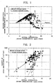
- Fig. 1 is a graph representing experimental results showing the relationship between the initial interstitial oxygen concentration and the residual interstitial oxygen concentration of a CZ wafer subjected to a usual oxygen precipitation heat treatment.
- Fig. 2 is a graph representing experimental results showing the relationship between the initial interstitial oxygen concentration and the density of precipitates of a CZ wafer subjected to a usual oxygen precipitation heat treatment.
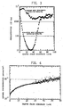
- Fig. 3 is a graph showing the relationship between the depth from surface and the resistivities before and after heat treatment in a conventional silicon wafer.
- Fig. 4 is a graph showing the relationship between the depth from surface and the absolute value of oxygen concentration in a conventional silicon wafer.
- Fig. 5 is a schematic view showing precipitate distribution along the depth direction in a conventional silicon wafer.
- the inventors of the present invention applied a three-step heat treatment usually performed as a heat treatment for obtaining an interstitial oxygen concentration of 8 ppma or less to a CZ silicon wafer of high resistivity as a trial.
- the heat treatment of the third step for growing oxide precipitates was performed by divided two stages at temperatures of 800°C and 1000°C.
- the inventors of the present invention measured and examined distribution of absolute value of oxygen concentration along the depth direction in a wafer after the three-step heat treatment, in which the resistivity decreased, by using a secondary ion mass spectroscopy (SIMS) apparatus (Fig. 4). Further, the wafer was subjected to angle polishing and preferential etching, and then distribution of oxide precipitates (etch pits) along the depth direction was observed. The results are schematically shown in Fig. 5.
- SIMS secondary ion mass spectroscopy
- a region of about 20 ⁇ m from the surface is the DZ layer
- a deeper region of a depth of about 30 ⁇ m or more from the surface is the oxide precipitate layer
- a region between them of a depth of about 20 to 30 ⁇ m from the surface is the transition region (a region that does not fully become a DZ layer, in which a few oxide precipitates exist) in the wafer referred to in Fig. 4.
- a region around the transition region corresponded to a region in which resistivity was extremely decreased after the heat treatment simulating a device production heat treatment.
- the interstitial oxygen concentration in this region was measured later by infrared absorption spectroscopy, it was found to be a portion where the interstitial oxygen concentration exceeded 8 ppma (4 x 10 17 atoms/cm 3 ).
- the interstitial oxygen concentration of not only the DZ layer and the oxide precipitate layer but also the transition region between the both should be made to be 8 ppma or less, or if the aforementioned transition region could be made to have a width as narrow as possible and a profile as sharp as possible, the amount of interstitial oxygen as the whole transition region would become small, and thus the influence of oxygen that became donor could also be made small.
- the inventors of the present invention investigated production conditions for a silicon wafer that satisfy these requirements.
- they conceived doping of a silicon single crystal with nitrogen during the growth of the crystal by the CZ method. That is, it has been pointed out that, if nitrogen is doped in a silicon single crystal, the aggregation of oxygen atoms in the silicon is promoted, and thus the oxide precipitate density increases (T. Abe and H. Takeno, Mat. Res. Soc. Symp. Proc. Vol. 262, 3, 1992). It is thought that this effect is obtained because the aggregation process of oxygen atoms is shifted from that consisting of homogenous nucleus formation to that consisting of heterogenous nucleus formation utilizing nitrogen impurities as nuclei. Furthermore, it is also known that, if nitrogen is doped in a single crystal, sizes of crystal defects such as COPs become small.
- a silicon single crystal is doped with nitrogen during the growth thereof, formation and growth of oxygen precipitation nuclei can be attained to a certain extent during the crystal growth, thus it is expected that the precipitation of interstitial oxygen is promoted also in the transition region between the DZ layer and the oxide precipitate layer to sufficiently reduce the interstitial oxygen concentration, and it is considered that the width of the transition region can be narrowed so that the region should have a sharp profile. Further, it is considered that, since sizes of grown-in defects such as COPs are made small by the nitrogen doping, it becomes easier to eliminate them by a subsequent heat treatment. Therefore, the inventors of the present invention performed the following experiments concerning nitrogen-doped CZ wafers.
- Fig. 1 shows experimental results representing relationship between the initial interstitial oxygen concentration and the residual interstitial oxygen concentration in various CZ wafers having an initial interstitial oxygen concentration of 8 to 21 ppma after they were subjected to usual heat treatments for oxygen precipitation, i.e., a heat treatment at 780°C for 3 hours and a heat treatment at 1000°C for 16 hours under a nitrogen atmosphere (containing 3% of oxygen).
- a heat treatment at 780°C for 3 hours i.e., a heat treatment at 780°C for 3 hours and a heat treatment at 1000°C for 16 hours under a nitrogen atmosphere (containing 3% of oxygen).
- Two kinds of the nitrogen concentrations i.e., 1 x 10 13 to 9 x 10 13 number/cm 3 and no nitrogen doping, were used.
- Fig. 2 shows experimental results representing relationship between the initial interstitial oxygen concentration and the density of precipitates in various CZ wafers having an initial interstitial oxygen concentration of 4 to 19 ppma after they are subjected to usual heat treatments for oxygen precipitation, i.e., a heat treatment at 780°C for 3 hours and a heat treatment at 1000°C for 16 hours under a nitrogen atmosphere (containing 3% of oxygen), angle polishing and preferential etching, in which the measured density of precipitates in the oxygen precipitation region was converted into volume density.
- Two kinds of the nitrogen concentrations i.e., 1 x 10 13 to 9 x 10 13 number/cm 3 and no nitrogen doping, were used.
- the oxide precipitate density is markedly increased by the nitrogen doping, even if the initial interstitial oxygen concentration is the same. It can be seen that, in particular, even with a low initial interstitial oxygen concentration of 8 ppma or less, a precipitate density of 1 x 10 8 number/cm 3 can be obtained by the nitrogen doping.
- oxide precipitates are not substantially formed in a non-nitrogen-doped wafer of a low oxygen concentration having an initial interstitial oxygen concentration of 8 ppma or less, but when nitrogen was doped, oxygen precipitation nuclei (oxide precipitates) stable at a high temperature had been already formed in the as-grown state, and therefore oxide precipitates having sizes detectable as oxide precipitates were obtained even by an extremely small degree of nucleus growth in such an extent that the growth could not be detected as an amount of precipitated oxygen after the subsequent heat treatment.
- the inventors of the present invention considered that, if elimination of COPs and formation of oxide precipitates were performed simultaneously under conditions under which COPs were easily eliminated, and oxide precipitates are sufficiently formed, i.e., by using a temperature not so high as the DZ formation heat treatment of the conventional three-step heat treatment (high temperature heat treatment) instead of the heat treatments used in the aforementioned experiments, the transition region could be made to have a narrow width and a sharp profile, as a result, high resistivity could be maintained, and the desired CZ silicon wafer could eventually be obtained, and they accomplished the present invention.
- a silicon single crystal ingot is pulled by the known CZ method or the known MCZ method where a single crystal is pulled while a magnetic field is applied to a melt in the CZ method to control convection of the silicon melt, so that the silicon single crystal ingot should have a desired high resistivity of 100 ⁇ cm or more and an initial interstitial oxygen concentration of 10 to 25 ppma.
- These pulling methods are methods comprising bringing a seed crystal into contact with a melt of polycrystalline silicon raw material contained in a quartz crucible and slowly pulling the seed crystal with rotation to allow growth of a single crystal ingot of a desired diameter.
- a desired initial interstitial oxygen concentration can be obtained by using conventional techniques.
- a crystal having a desired oxygen concentration can be obtained by suitably adjusting parameters such as rotational speed of the crucible, flow rate of introduced gas, atmospheric pressure, temperature distribution and convection of silicon melt and strength of the magnetic field to be applied.
- the parameters to be controlled during the crystal growth are similar to those for the case where the interstitial oxygen concentration is 10 to 25 ppma (also referred to as “high oxygen concentration” hereafter) is pulled as mentioned above.
- the MCZ method is usually used.
- the simultaneous doping with nitrogen as well as oxygen can be easily performed by preliminarily adding nitride such as wafers having nitride films into the raw material polycrystal contained in a quartz crucible.
- concentration of nitrogen to be doped in a pulled crystal can be calculated from the amount of nitride introduced into the raw material polycrystal or crucible, the segregation coefficient of nitrogen and so forth.
- the CZ silicon single crystal ingot obtained as described above is sliced by using a cutting machine such as a wire saw or inner diameter slicer, and subjected to steps of chamfering, lapping, etching, polishing and so forth to be processed into CZ silicon single crystal wafers according to conventional techniques.
- a cutting machine such as a wire saw or inner diameter slicer
- steps of chamfering, lapping, etching, polishing and so forth to be processed into CZ silicon single crystal wafers according to conventional techniques.
- these steps are mere examples, and there may be used various other steps such as cleaning step and heat treatment step.
- the steps are used with suitable modification including the alteration of the order of steps, omission of some steps and so forth according to the purpose.
- a heat treatment that provides a residual interstitial oxygen concentration of 8 ppma or less is applied.
- the heat treatment that provides a residual interstitial oxygen concentration of 8 ppma or less used in this case cannot be necessarily specified, because the residual interstitial oxygen concentration varies depending on the initial interstitial oxygen concentration and thermal history during crystal growth of a wafer to be subjected to a heat treatment. However, it can be determined by experiments according to the initial interstitial oxygen concentration, thermal history and so forth.
- the heat treatment for eliminating COPs is preferably a heat treatment at a high temperature in hydrogen gas, argon gas or a mixed gas thereof.
- the heat treatment temperature is preferably 1000 to 1200°C. Even with such a relatively low temperature, COPS can be sufficiently eliminated, because the sizes of COPs are made small by the effect of the nitrogen doping, and interstitial oxygen can also be reduced by out-diffusion thereof. Further, if hydrogen gas, argon gas or a mixed gas thereof is used, the out-diffusion profile of oxygen abruptly changes at the wafer surface, and thus a transition region having a sharper profile can be formed.
- the aforementioned heat treatment can also be dividedly performed, for example, with two stages at 1200°C and 1000°C, to sufficiently eliminate COPs at a high temperature of the first stage, and then sufficiently grow oxide precipitates at a low temperature of the second stage.
- COPs can be easily eliminated by a heat treatment at a temperature as high as possible within a range that provides sufficient formation of oxide precipitates.
- the temperature is preferably 1000 to 1200°C.
- These heat treatments can be performed by using a usual vertical type furnace or a usual horizontal type furnace (diffusion furnace), which enables a simultaneous heat treatment of many wafers.
- Silicon wafers having nitride films were introduced into raw material polycrystal, and a nitrogen-doped silicon single crystal was pulled by the CZ method (without applying magnetic field).
- the silicon single crystal was processed by a usual method to produce a CZ silicon wafer having a diameter of 200 mm, an initial interstitial concentration of 18 ppma (JEIDA), a nitrogen concentration of 8 x 10 13 number/cm 3 (calculated value) and a resistivity of 2500 ⁇ cm.
- This wafer was subjected to a heat treatment at 1100°C for 2 hours and a heat treatment at 1000°C for 16 hours under a 100% argon atmosphere and further subjected to heat treatments simulating a device production process (heat treatments at 1200°C for 1 hour and at 450°C for 5 hours) under a nitrogen atmosphere (mixed with 3% of oxygen) in a vertical type heat treatment furnace.
- heat treatments at 1200°C for 1 hour and at 450°C for 5 hours
- nitrogen atmosphere mixed with 3% of oxygen
- the wafer after the heat treatments was subjected to angle lapping, and then resistivity was measured by the spreading resistance measurement method for a portion from the surface to a depth of 100 ⁇ m. As a result, it was confirmed that every region in the wafer had a resistivity of 2000 ⁇ cm or more.
- the surface undergone angle polishing was subjected to preferential etching and observed by using a optical microscope. As a result, the transition region had a narrow width of about 5 ⁇ m, i.e., a sharp profile, and the defect density in the oxygen precipitation region was a sufficient value, i.e., 5 to 8 x 10 9 number/cm 3 . That is, it can be seen that the silicon wafer of Example 1 was a DZ-IG wafer scarcely influenced by the resistivity reduction due to the oxygen donor and having sufficient gettering ability.
- the surface of the wafer after the heat treatments was polished by about 3 ⁇ m, and density of COPs existing on the polished surface and having a size of 0.12 ⁇ m or more as the diameter were measured by using a particle counter (SP1, produced by KLA Tencor Corporation).
- SP1 produced by KLA Tencor Corporation
- the measured COP density was an extremely low density, i.e., 0.06 number/cm 2 .
- a silicon single crystal was pulled with the same conditions as those of Example 1 except that nitrogen was not doped, and processed by a usual method to produce a CZ silicon wafer having a diameter of 200 mm, an initial interstitial concentration of 18 ppma (JEIDA) and a resistivity of 2500 ⁇ cm.
- JEIDA initial interstitial concentration of 18 ppma
- This wafer was subjected to a three-step heat treatment (DZ-IG treatment) comprising a heat treatment at 1150°C for 4 hours, a heat treatment at 650°C for 6 hours and a heat treatment at 1000°C for 16 hours under a nitrogen atmosphere (mixed with 3% of oxygen) and further subjected to heat treatments simulating a device production process (heat treatments at 1200°C for 1 hour and at 450°C for 5 hours) in a vertical type heat treatment furnace.
- DZ-IG treatment three-step heat treatment
- the residual interstitial oxygen concentration was measured by infrared absorption spectroscopy for the whole wafer, and it was confirmed that the residual interstitial oxygen concentration in the wafer was 8 ppma or less.
- the wafer after the heat treatments was subjected to angle lapping, and then resistivity was measured by the spreading resistance measurement method for a portion from the surface to a depth of 100 ⁇ m. As a result, it was confirmed that the resistivity was decreased to ten and several ⁇ cm in a region of a depth of 20 to 40 ⁇ m from the surface. Subsequently, the surface undergone angle polishing was subjected to preferential etching and observed by using a opical microscope. As a result, the region in which resistivity was decreased substantially corresponded to the transition region.
- the interstitial oxygen concentration was confirmed again by infrared absorption spectroscopy only for the transition region, it was found that the region is a portion where the interstitial oxygen concentration exceeded 8 ppma (4 x 10 17 atom/cm 3 ). Based on this, it is considered that the amount of interstitial oxygen becoming donor was large in that portion, thus the conductivity type was reversed from p-type into n-type, and therefore the resistivity was further decreased.
- the measurement of the interstitial oxygen concentration in the transition region by infrared absorption spectroscopy can be performed by, for example, a measurement method of using a bonded wafer obtained by eliminating the DZ layer by polishing, bonding the obtained surface to an FZ wafer and eliminating the oxide precipitate layer.
- the surface of the wafer after the heat treatments was polished by about 3 ⁇ m, and density of COPs existing on the polished surface and having a size of 0.12 ⁇ m or more as the diameter were measured by using a particle counter (SP1, produced by KLA Tencor Corporation).
- SP1 produced by KLA Tencor Corporation
- the measured COP density was 4.3 number/cm 2 , which was substantially the same density as the density before the heat treatments.
- Silicon wafers having nitride films were introduced raw material polycrystal, and a nitrogen-doped silicon single crystal was pulled by the MCZ method.
- the silicon single crystal was processed by a usual method to produce a CZ silicon wafer having a diameter of 200 mm, an initial interstitial concentration of 6 ppma (JEIDA), a nitrogen concentration of 9 x 10 13 number/cm 3 (calculated value) and a resistivity of 1500 ⁇ cm.
- This wafer was subjected to a heat treatment at 800°C for 4 hours under a nitrogen atmosphere and a heat treatment at 1100°C for 16 hours under an argon atmosphere (mixed with 3% of hydrogen) and further subjected to heat treatments simulating a device production process (heat treatments at 1200°C for 1 hour and at 450°C for 5 hours) in a vertical type heat treatment furnace.
- heat treatments at 1200°C for 1 hour and at 450°C for 5 hours in a vertical type heat treatment furnace.
- the residual interstitial oxygen concentration was measured by infrared absorption spectroscopy for the whole wafer, and it was confirmed that the residual interstitial oxygen concentration in the wafer was 8 ppma or less.
- the wafer after the heat treatments was subjected to angle lapping, and resistivity was measured by the spreading resistance measurement method for a portion from the surface to a depth of 100 ⁇ m. As a result, it was confirmed that every region in the wafer had a resistivity of 1000 ⁇ cm or more.
- the surface undergone angle polishing was subjected to preferential etching and observed by using a optical microscope. As a result, the defect density in the oxide precipitate region was a sufficient value, i.e., 1 to 5 x 10 8 number/cm 3 . That is, it can be seen that the silicon wafer of Example 2 was also a DZ-IG wafer scarcely influenced by the resistivity reduction due to the oxygen donor and having sufficient gettering ability, even though the silicon single crystal was grown with a low oxygen concentration.
- the surface of the wafer after the heat treatments was polished by about 3 ⁇ m, and density of COPs existing on the polished surface and having a size of 0.12 ⁇ m or more as the diameter were measured by using a particle counter (SP1, produced by KLA Tencor Corporation).
- SP1 produced by KLA Tencor Corporation
- the measured COP density was extremely low density, i.e., 0.1 number/cm 2 .
- a silicon single crystal was pulled with the same conditions as those of Example 2 except that nitrogen was not doped, and processed by a usual method to produce a CZ silicon wafer having a diameter of 200 mm, an initial interstitial concentration of 6 ppma (JEIDA) and a resistivity of 1500 ⁇ cm.
- JEIDA initial interstitial concentration of 6 ppma
- This wafer was subjected to a three-step heat treatment (DZ-IG treatment) comprising a heat treatment at 1150°C for 4 hours, a heat treatment at 650°C for 6 hours and a heat treatment at 1000°C for 16 hours under a nitrogen atmosphere (mixed with 3% of oxygen) and further subjected to heat treatments simulating a device production process (heat treatments at 1200°C for 1 hour and at 450°C for 5 hours) in a vertical type heat treatment furnace.
- DZ-IG treatment three-step heat treatment
- the residual interstitial oxygen concentration was measured by infrared absorption spectroscopy for the whole wafer, and it was confirmed that the residual interstitial oxygen concentration in the wafer was 8 ppma or less.
- the wafer after the heat treatments was subjected to angle lapping, and resistivity was measured by the spreading resistance measurement method for a portion from the surface to a depth of 100 ⁇ m. As a result, it was confirmed that every region in the wafer had a resistivity of 1000 ⁇ cm or more.
- the defect density in the oxide precipitate region was found to be extremely low, i.e., 1 to 5 x 10 6 number/cm 3 .
- the silicon wafer of Comparative Example 2 was a wafer not substantially influenced by the resistivity reduction due to the oxygen donor, it was a wafer that did not have sufficient gettering ability, since the silicon single crystal was grown with a low oxygen concentration, and thus oxygen precipitation was unlikely to occur in the bulk portion.
- the surface of the wafer after the heat treatments was polished by about 3 ⁇ m, and density of COPs existing on the polished surface and having a size of 0.12 ⁇ m or more as the diameter were measured by using a particle counter (SP1, produced by KLA Tencor Corporation).
- SP1 produced by KLA Tencor Corporation
- the measured COP density was 4.0 number/cm 2 , which was substantially the same density as the density before the heat treatments.
Landscapes
- Chemical & Material Sciences (AREA)
- Engineering & Computer Science (AREA)
- Crystallography & Structural Chemistry (AREA)
- Materials Engineering (AREA)
- Metallurgy (AREA)
- Organic Chemistry (AREA)
- Crystals, And After-Treatments Of Crystals (AREA)
- Liquid Deposition Of Substances Of Which Semiconductor Devices Are Composed (AREA)
Abstract
The present invention provides a method for
producing a silicon wafer, which comprises growing a
silicon single crystal ingot having a resistivity of
100 Ω·cm or more and an initial interstitial oxygen
concentration of 10 to 25 ppma and doped with
nitrogen by the Czochralski method, processing the
silicon single crystal ingot into a wafer, and
subjecting the wafer to a heat treatment so that a
residual interstitial oxygen concentration in the
wafer should become 8 ppma or less, and a method for
producing a silicon wafer, which comprises growing a
silicon single crystal ingot having a resistivity of
100 Ω·cm or more and an initial interstitial oxygen
concentration of 8 ppma or less and doped with
nitrogen by the Czochralski method, processing the
silicon single crystal ingot into a wafer, and
subjecting the wafer to a heat treatment to form an
oxide precipitate layer in a bulk portion of the
wafer, as well as silicon wafers produced by these
production methods. Thus, there is provided a DZ-IG
silicon wafer in which a DZ layer of high quality is
formed, and which can maintain high resistivity even
if the wafer is subjected to a heat treatment for
device production.
Description
The present invention relates to a technique by
which a DZ-IG silicon wafer having high resistivity
and also having high gettering ability can surely be
obtained.
Silicon wafers of high resistivity produced by
the floating zone method (FZ method) have
conventionally been used for power devices such as
high-voltage power devices and thyristors. However,
it is difficult to produce a silicon wafer having a
large diameter of 200 mm or more by the FZ method,
and the radial resistivity distribution of usual FZ
wafers is inferior to that of CZ wafers. Therefore,
silicon wafers produced by the CZ method will be
promising in the future, because wafers of excellent
radial resistivity distribution can be produced by
the CZ method, and in addition, wafers of a large
size having a diameter of 200 mm or more can
sufficiently be produced by the method.
In recent years, in particular, reduction of
parasitic capacity is required in semiconductor
devices for mobile communications and the latest C-MOS
devices. For this reason, a silicon wafer of
high resistivity and a large diameter comes to be
needed. Moreover, the effect of using a high
resistivity substrate on reduction of transmission
loss of signals and parasitic capacity in Schottky
barrier diodes has been reported. Furthermore,
although the so-called SOI (Silicon On Insulator)
wafer may be used in order to obtain further higher
performance of the aforementioned semiconductor
devices, it is required to use a wafer of high
resistivity produced by the CZ method as a base wafer
even when semiconductor devices are produced by using
the SOI wafer in order to obtain a larger diameter of
wafer or solve the problem of transmission loss of
signals or the like.
However, since the CZ method utilizes a
crucible made of quartz, not a small amount of oxygen
(interstitial oxygen) is introduced into a silicon
crystal. Although each of such oxygen atoms is
usually electrically neutral, if they are subjected
to a heat treatment at a low temperature of around
350 to 500°C, a plurality of them gather to release
electrons and become electrically active oxygen
donors. Therefore, if a wafer obtained by the CZ
method is subsequently subjected to a heat treatment
at about 350 to 500°C in the device production
process and so forth, there arises a problem that
resistivity of a high resistivity CZ wafer is reduced
due to the formation of the oxygen donors.
In order to prevent the resistivity reduction
due to the above oxygen donors and obtain a silicon
wafer of high resistivity, methods for producing a
silicon single crystal having a low interstitial
oxygen concentration from an initial stage of the
crystal growth by the magnetic field-applied CZ
method (MCZ method) were proposed (refer to Japanese
Patent Publication (Kokoku) No. 8-10695 and Japanese
Patent Laid-open Publication (Kokai) No. 5-58788).
Further, there has also been proposed a method
conversely utilizing the phenomenon of the oxygen
donor formation, wherein a P-type silicon wafer of a
low impurity concentration and low oxygen
concentration is subjected to a heat treatment at 400
to 500°C to generate oxygen donors, and P-type
impurities in the P-type silicon wafer is compensated
by these oxygen donors so that the wafer should be
converted into N-type to produce an N-type silicon
wafer of high resistivity (refer to Japanese Patent
Publication No. 8-10695).
However, a silicon single crystal of a low
interstitial oxygen concentration produced by the MCZ
method or the like as mentioned above suffers from a
drawback that the density of bulk defects generated
by a heat treatment in the device production process
becomes low, and thus sufficient gettering effect
will be unlikely to be obtained. In devices of a
high integration degree, it is essential to impart
gettering effect by a certain amount of oxygen
precipitation.
Further, the method of obtaining a silicon
wafer of N-type by generating oxygen donors by a heat
treatment and compensating P-type impurities in the
wafer to convert it into N-type is a complicated
method that requires a heat treatment for a long
period of time. Moreover, this method cannot provide
a P-type silicon wafers. In addition, this method
also has a drawback that resistivity of wafers
obtained by this method may vary depending on a
subsequent heat treatment. Furthermore, in this
method, in case of high interstitial oxygen
concentration, it becomes difficult to control the
wafer resistivity. Therefore, this method suffers
from a drawback that a low initial concentration of
interstitial oxygen in a silicon wafer must be used,
and thus the gettering effect of the wafer becomes
low.
In order to solve these problems, the
applicants of the present application proposed, in a
previous application (Japanese Patent Application No.
11-241370, PCT/JP00/01124), a method for producing a
silicon wafer, which comprises growing a silicon
single crystal ingot having a resistivity of 100 Ω·
cm or more and an initial interstitial oxygen
concentration of 10 to 25 ppma (JEIDA: Japan
Electronic Industry Development Association) by the
Czochralski method, processing the silicon single
crystal ingot into a wafer, and subjecting the wafer
to an oxygen precipitation heat treatment so that a
residual interstitial oxygen concentration in the
wafer should become 8 ppma or less. According to
this method, a CZ wafer of high resistivity of which
resistivity is unlikely to decrease even when the
wafer is subjected to a heat treatment for device
production. Therefore, if this wafer is used as, for
example, a base wafer of SOI wafer, devices of
extremely high performance for mobile communications
can be obtained.
On the other hand, it is considered that, in
order to realize a wafer having performance of the
same level as the SOI wafer by using a bulk wafer, of
which production cost is more inexpensive compared
with SOI wafer, so to speak "high resistivity DZ-IG
wafer" of a structure having a DZ layer (Denuded Zone
layer) sufficiently made defect free on a surface of
such a high resistivity CZ wafer is required.
Although there has conventionally been the so-called
DZ-IG wafer, which is obtained by subjecting a CZ
silicon wafer having usual resistivity to a DZ-IG
(Intrinsic Gettering) treatment, there has not been
conceived to apply this technique to a high
resistivity CZ wafer at all. Therefore, the
applicant of the present application also disclosed a
method for obtaining a high resistivity DZ-IG wafer
by a heat treatment that makes the aforementioned
interstitial oxygen concentration 8 ppma or less in
the previous application (Japanese Patent Application
No. 11-241370).
As the DZ-IG treatment applied to a wafer of
usual resistivity, a three-step heat treatment is
generally used. Supersaturated oxygens in the
vicinity of a wafer surface are out-diffused by a
first step high temperature heat treatment at 1100°C
or higher, a low temperature heat treatment at around
650°C is performed as a second step heat treatment to
form oxygen precipitation nuclei, and a moderate
temperature heat treatment is performed at about
1000°C as the third step heat treatment to allow
growth of the oxide precipitates. By such a three-step
heat treatment, an oxide precipitate region is
formed in the wafer, and thus a DZ layer in which
oxide precipitates do not exist is formed in the
vicinity of surface of the front side or back side.
Therefore, the applicants of the present
application applied the same heat treatment as the
above heat treatment as the heat treatment for
obtaining an interstitial oxygen concentration of 8
ppma or less. As a result, it was found that a high
resistivity DZ-IG wafer having a high resistivity of
100 Ω·cm or more and having a DZ layer free from
crystal defects near the surface and an oxide
precipitate layer in which oxide precipitates are
sufficiently precipitated could be obtained.
It was considered that such a high resistivity
DZ-IG wafer could sufficiently serve as an
alternative of SOI wafers for mobile communications.
However, subsequent investigations revealed that, if
such a DZ-IG wafer was subjected to a heat treatment
during the device production process, the resistivity
near the wafer surface was extremely reduced as the
case may be, and thus sufficient high resistivity may
not be obtained.
Further, it was also found that, although the
DZ layer formed by such a heat treatment was surely
made defect free as for defects originated from oxide
precipitates, grown-in defects called COP (Crystal
Originated Particle) were not eliminated and still
remained.
COP is a void of 0.1 µm order size formed by
aggregation of excessive vacancies during the growth
of CZ silicon single crystals, and the internal
surface thereof is covered with a thin oxide film.
Further, it is known that, if a device is formed on a
portion where such grown-in defects exist, device
characteristics such as oxide dielectric breakdown
voltage are degraded.
The present invention was accomplished in order
to solve these problems, and its object is to provide
a method for producing a silicon wafer in which a DZ
layer of high quality made defect free not only for
oxide precipitates but also for COPs is formed in the
vicinity of the wafer surface, oxide precipitates are
formed in the bulk portion at a sufficient density
and thereby high gettering ability can be obtained,
and which can maintain high resistivity even after
the wafer is subjected to a heat treatment for device
production, and thereby provide a high resistivity
DZ-IG wafer of high quality at a thus-far unknown
level, which can serve as an alternative of SOI wafer
for mobile communications.
In order to achieve the aforementioned object,
the present invention provides a method for producing
a silicon wafer, which comprises growing a silicon
single crystal ingot having a resistivity of 100 Ω·
cm or more and an initial interstitial oxygen
concentration of 10 to 25 ppma and doped with
nitrogen by the Czochralski method, processing the
silicon single crystal ingot into a wafer, and
subjecting the wafer to a heat treatment so that a
residual interstitial oxygen concentration in the
wafer should become 8 ppma or less.
If nitrogen is doped in a silicon single
crystal as described above, sizes of grown-in defects
(COPS) become small, and it becomes easy to eliminate
them by a heat treatment. In addition, formation and
growth of oxygen precipitation nuclei can be attained
to a certain degree during the crystal growth. Thus,
it becomes possible to form a DZ layer of high
quality by a heat treatment at a temperature lower
than that of the conventional DZ-IG treatment by a
three-step heat treatment (formation of DZ layer
(high temperature) + formation of precipitation
nuclei (low temperature) + growth of precipitates
(moderate temperature)), and it also becomes possible
to grow oxide precipitates of a sufficient density in
the bulk portion by a heat treatment for a short
period of time. Therefore, the transition region
between the DZ layer and the oxide precipitate region
can be made to have a narrow and sharp profile, and
the amount of interstitial oxygen in the whole
transition region can be made small. Thus, the
influence of oxygen acting as donor can be reduced.
Furthermore, it also becomes possible to enlarge the
acceptable range of the initial interstitial oxygen
concentration that can provide an interstitial oxygen
concentration of 8 ppma (JEIDA: Japan Electronic
Industry Development Association Standard) or less
for a specific heat treatment.
The present invention also provides a method
for producing a silicon wafer, which comprises
growing a silicon single crystal ingot having a
resistivity of 100 Ω·cm or more and an initial
interstitial oxygen concentration of 8 ppma or less
and doped with nitrogen by the Czochralski method,
processing the silicon single crystal ingot into a
wafer, and subjecting the wafer to a heat treatment
to form an oxide precipitate layer in a bulk portion
of the wafer.
If nitrogen is doped in a silicon single
crystal as described above, the oxygen precipitation
is more promoted when the wafer is subjected to an
oxygen precipitation heat treatment compared with a
wafer not doped with nitrogen, even if the wafer is a
wafer of low oxygen content having an initial
interstitial oxygen concentration of 8 ppma or less,
and thus it becomes possible to form oxide
precipitates at a sufficient density. Moreover,
since the wafer contains oxygen at a low
concentration, the oxide films on the internal
surfaces of COPs formed during the crystal growth
become thin, and it becomes easy to eliminate COPs by
a heat treatment. For these reasons, it becomes
possible to form a DZ layer of high quality and oxide
precipitates at a sufficient density in the bulk
portion by a heat treatment at a relatively lower
temperature for a shorter period of time compared
with those used in the conventional techniques.
Furthermore, since the interstitial oxygen
concentration is originally 8 ppma or less,
substantially no fluctuation of resistivity due to
oxygen acting as donor is caused in the device
production process. Moreover, the method also has an
advantage that the problem of low resistance of the
wafer to slip dislocations generated by a heat
treatment due to the low oxygen concentration in a
wafer not doped with nitrogen can also be covered by
the use of the milder heat treatment conditions (low
temperature and short time).
In the aforementioned methods, nitrogen is
preferably doped at a concentration of 1 x 10¹² to 5
x 1015 number/cm3.
This is because, if the nitrogen concentration
is less than 1 x 10¹² number/cm3, the effect is not so
remarkable compared with a case not using the
nitrogen doping, and if it exceeds 5 x 10¹⁵ number/cm3,
the single crystallization during the pulling of the
crystal may be inhibited, or it may make continuous
operation unstable. More preferably, the nitrogen
concentration should be less than 1 x 10¹⁴ number/cm3.
This is because, if the nitrogen concentration is 1 x
1014 number/cm3 or more, the amount of oxygen-nitrogen
donors formed by a heat treatment at around 600°C
increases, and they may reduce the resistivity. That
is, it is known that about 10% of the doped nitrogen
contributes to the formation of oxygen-nitrogen
donors, and a doping amount of 1 x 10¹⁴ number/cm3 may
form 1 x 10¹³ number/cm3 of oxygen-nitrogen donors.
If all of these donors are activated, there is caused
fluctuation of the resistivity in the order of
several hundreds Ω·cm. However, it can be conversely
said that, if the amount of the generated donors is
the above level or less, they show substantially no
influence.
Further, in the aforementioned method, the heat
treatment is preferably performed at a temperature of
1000 to 1200°C for 1 to 20 hours in hydrogen gas,
argon gas or a mixed gas atmosphere of hydrogen gas
and argon gas.
If the heat treatment is performed in hydrogen
gas, argon gas or a mixed gas atmosphere thereof as
described above, grown-in defects at the wafer
surface and in the vicinity of the wafer surface can
be effectively eliminated, and the oxide precipitates
in the bulk portion can be grown at the same time.
In this case, if the heat treatment temperature is
lower than 1000°C, a heat treatment for a long period
of time exceeding 20 hours is required in order to
sufficiently eliminate the grown-in defects. Further,
although the grown-in defects can be sufficiently
eliminated by a heat treatment for about 1 hour at a
heat treatment temperature of 1200°C, if the
temperature exceeds 1200°C, the oxygen precipitation
nuclei formed by the effect of the nitrogen doping
during the crystal growth become likely to melt again,
and thus it becomes difficult to obtain a sufficient
oxide precipitate density after the heat treatment.
Therefore, the heat treatment temperature is
preferably 1000 to 1200°C.
A silicon wafer produced by the production
method of the present invention described above has a
high resistivity of 100 Ω·cm or more and a low
interstitial oxygen concentration of 8 ppma or less.
Therefore, it can be a high resistivity DZ-IG wafer
of high quality in which resistivity is not reduced
by oxygen acting as donor during the device
production process, and which contains substantially
no grown-in defect in the DZ layer near the wafer
surface.
As explained above, according to the present
invention, there can be obtained a CZ silicon wafer
in which fluctuation of resistivity due to
interstitial oxygen acting as donor is suppressed
even after the wafer is subjected to a heat treatment
for device production. This effect is extremely
effective for a high resistivity CZ wafer having a
resistivity of 100 Ω·cm or more, and it enables use
of the wafer as an alternative of SOI wafer for
mobile communications.
Fig. 1 is a graph representing experimental
results showing the relationship between the initial
interstitial oxygen concentration and the residual
interstitial oxygen concentration of a CZ wafer
subjected to a usual oxygen precipitation heat
treatment.
Fig. 2 is a graph representing experimental
results showing the relationship between the initial
interstitial oxygen concentration and the density of
precipitates of a CZ wafer subjected to a usual
oxygen precipitation heat treatment.
Fig. 3 is a graph showing the relationship
between the depth from surface and the resistivities
before and after heat treatment in a conventional
silicon wafer.
Fig. 4 is a graph showing the relationship
between the depth from surface and the absolute value
of oxygen concentration in a conventional silicon
wafer.
Fig. 5 is a schematic view showing precipitate
distribution along the depth direction in a
conventional silicon wafer.
Hereafter, the present invention will be
explained in detail.
As described above, in order to obtain a "high
resistivity DZ-IG wafer" that can realize, as a bulk
wafer, performance at a level equivalent to that of
an SOI wafer for mobile communications utilizing a
high resistivity wafer as the base wafer, the
inventors of the present invention applied a three-step
heat treatment usually performed as a heat
treatment for obtaining an interstitial oxygen
concentration of 8 ppma or less to a CZ silicon wafer
of high resistivity as a trial. The heat treatment
of the third step for growing oxide precipitates was
performed by divided two stages at temperatures of
800°C and 1000°C.
As a result, in the wafer immediately after the
three-step heat treatment, a DZ layer was formed in
the vicinity of the wafer surface while the high
resistivity was maintained, and an IG layer (oxide
precipitate region) was formed in the bulk portion.
Thus, a desired high resistivity DZ-IG wafer was
obtained (Fig. 3 (a)). However, when a heat
treatment simulating a device production heat
treatment was applied to this wafer, it was found
that the resistivity might extremely decreased in the
vicinity of the wafer surface as the case may be (Fig.
3 (b)).
It was expected that the resistivity decrease
was caused because interstitial oxygen existing in
the wafer became donor. Therefore, the inventors of
the present invention measured and examined
distribution of absolute value of oxygen
concentration along the depth direction in a wafer
after the three-step heat treatment, in which the
resistivity decreased, by using a secondary ion mass
spectroscopy (SIMS) apparatus (Fig. 4). Further, the
wafer was subjected to angle polishing and
preferential etching, and then distribution of oxide
precipitates (etch pits) along the depth direction
was observed. The results are schematically shown in
Fig. 5.
From the results shown in Figs. 4 and 5, it can
be seen that a region of about 20 µm from the surface
is the DZ layer, a deeper region of a depth of about
30 µm or more from the surface is the oxide
precipitate layer, and a region between them of a
depth of about 20 to 30 µm from the surface is the
transition region (a region that does not fully
become a DZ layer, in which a few oxide precipitates
exist) in the wafer referred to in Fig. 4. A region
around the transition region corresponded to a region
in which resistivity was extremely decreased after
the heat treatment simulating a device production
heat treatment. When the interstitial oxygen
concentration in this region was measured later by
infrared absorption spectroscopy, it was found to be
a portion where the interstitial oxygen concentration
exceeded 8 ppma (4 x 10¹⁷ atoms/cm3).
Furthermore, when COPs in a region of a depth
of several micrometers from the surface were measured
by using a particle counter before and after the
three-step heat treatment, there is almost no change
was observed, and thus it was confirmed that COPs
remained in the wafer surface portion.
That is, it is considered that, even if the
interstitial oxygen in the DZ layer near the surface
is out-diffused, and the interstitial oxygen
concentration in the bulk portion becomes
sufficiently low due to precipitation of oxygen as
oxide precipitates, the interstitial oxygen
concentration is still high in the transition region
between them even after the three-step heat treatment,
and therefore the resistivity is decreased by oxygen
becoming donor.
Therefore, it was considered that, for the
purpose of surely obtaining a high resistivity DZ-IG
wafer, the interstitial oxygen concentration of not
only the DZ layer and the oxide precipitate layer but
also the transition region between the both should be
made to be 8 ppma or less, or if the aforementioned
transition region could be made to have a width as
narrow as possible and a profile as sharp as possible,
the amount of interstitial oxygen as the whole
transition region would become small, and thus the
influence of oxygen that became donor could also be
made small. In addition, it was also considered that
it was necessary to decrease COPs in the DZ layer.
Therefore, the inventors of the present
invention investigated production conditions for a
silicon wafer that satisfy these requirements. As a
result, they conceived doping of a silicon single
crystal with nitrogen during the growth of the
crystal by the CZ method. That is, it has been
pointed out that, if nitrogen is doped in a silicon
single crystal, the aggregation of oxygen atoms in
the silicon is promoted, and thus the oxide
precipitate density increases (T. Abe and H. Takeno,
Mat. Res. Soc. Symp. Proc. Vol. 262, 3, 1992). It is
thought that this effect is obtained because the
aggregation process of oxygen atoms is shifted from
that consisting of homogenous nucleus formation to
that consisting of heterogenous nucleus formation
utilizing nitrogen impurities as nuclei. Furthermore,
it is also known that, if nitrogen is doped in a
single crystal, sizes of crystal defects such as COPs
become small.
Therefore, if a silicon single crystal is doped
with nitrogen during the growth thereof, formation
and growth of oxygen precipitation nuclei can be
attained to a certain extent during the crystal
growth, thus it is expected that the precipitation of
interstitial oxygen is promoted also in the
transition region between the DZ layer and the oxide
precipitate layer to sufficiently reduce the
interstitial oxygen concentration, and it is
considered that the width of the transition region
can be narrowed so that the region should have a
sharp profile. Further, it is considered that, since
sizes of grown-in defects such as COPs are made small
by the nitrogen doping, it becomes easier to
eliminate them by a subsequent heat treatment.
Therefore, the inventors of the present invention
performed the following experiments concerning
nitrogen-doped CZ wafers.
Fig. 1 shows experimental results representing
relationship between the initial interstitial oxygen
concentration and the residual interstitial oxygen
concentration in various CZ wafers having an initial
interstitial oxygen concentration of 8 to 21 ppma
after they were subjected to usual heat treatments
for oxygen precipitation, i.e., a heat treatment at
780°C for 3 hours and a heat treatment at 1000°C for
16 hours under a nitrogen atmosphere (containing 3%
of oxygen). Two kinds of the nitrogen concentrations,
i.e., 1 x 10¹³ to 9 x 10¹³ number/cm3 and no nitrogen
doping, were used.
From the results shown in Fig. 1, it can be
seen that if nitrogen is not doped, the residual
interstitial oxygen concentration cannot be made 8
ppma or less after the aforementioned heat treatments
unless the initial interstitial oxygen concentration
is 19 ppma or more, whereas if nitrogen is doped, the
range of acceptable initial interstitial oxygen
concentration is enlarged to the range of 15 ppma or
more. Further, it was confirmed that, by using a
longer heat treatment time, the range of acceptable
initial interstitial oxygen concentration could be
enlarged to the range of 10 ppma or more.
Fig. 2 shows experimental results representing
relationship between the initial interstitial oxygen
concentration and the density of precipitates in
various CZ wafers having an initial interstitial
oxygen concentration of 4 to 19 ppma after they are
subjected to usual heat treatments for oxygen
precipitation, i.e., a heat treatment at 780°C for 3
hours and a heat treatment at 1000°C for 16 hours
under a nitrogen atmosphere (containing 3% of oxygen),
angle polishing and preferential etching, in which
the measured density of precipitates in the oxygen
precipitation region was converted into volume
density. Two kinds of the nitrogen concentrations,
i.e., 1 x 10¹³ to 9 x 10¹³ number/cm3 and no nitrogen
doping, were used.
From the results shown in Fig. 2, it can be
seen that the oxide precipitate density is markedly
increased by the nitrogen doping, even if the initial
interstitial oxygen concentration is the same. It
can be seen that, in particular, even with a low
initial interstitial oxygen concentration of 8 ppma
or less, a precipitate density of 1 x 10⁸ number/cm3
can be obtained by the nitrogen doping.
Based on the results shown in Fig. 1 mentioned
above, it is considered that it is expected that
oxide precipitates are not substantially formed in a
non-nitrogen-doped wafer of a low oxygen
concentration having an initial interstitial oxygen
concentration of 8 ppma or less, but when nitrogen
was doped, oxygen precipitation nuclei (oxide
precipitates) stable at a high temperature had been
already formed in the as-grown state, and therefore
oxide precipitates having sizes detectable as oxide
precipitates were obtained even by an extremely small
degree of nucleus growth in such an extent that the
growth could not be detected as an amount of
precipitated oxygen after the subsequent heat
treatment.
From these results, it is expected that, as for
wafers obtained from a single crystal having an
initial interstitial oxygen concentration of about 10
to 25 ppma, if the crystal is grown with nitrogen
doping, the oxygen precipitation is promoted during
the subsequent heat treatment for oxygen
precipitation, thus the residual interstitial oxygen
concentration can be reduced also in the transition
region, and a sufficiently narrow and sharp profile
of the transition region can be obtained. Further,
it can be seen that, as also for wafers obtained from
a single crystal having an initial interstitial
oxygen concentration of 8 ppma or less, if nitrogen
is doped, sufficient oxygen precipitation can be
obtained by the subsequent heat treatment for oxygen,
and sufficient gettering effect can be secured.
Further, although the quality of the DZ layer,
especially the presence or absence of COP, was not
evaluated in the experiments described above, it is
known that sizes of COPs are made smaller by nitrogen
doping, and thus it becomes easier to eliminate them
by a heat treatment. Therefore, the inventors of the
present invention considered that, if elimination of
COPs and formation of oxide precipitates were
performed simultaneously under conditions under which
COPs were easily eliminated, and oxide precipitates
are sufficiently formed, i.e., by using a temperature
not so high as the DZ formation heat treatment of the
conventional three-step heat treatment (high
temperature heat treatment) instead of the heat
treatments used in the aforementioned experiments,
the transition region could be made to have a narrow
width and a sharp profile, as a result, high
resistivity could be maintained, and the desired CZ
silicon wafer could eventually be obtained, and they
accomplished the present invention.
The present inventions will be further
explained hereafter. However, the present invention
is not limited by these explanations.
First, a silicon single crystal ingot is pulled
by the known CZ method or the known MCZ method where
a single crystal is pulled while a magnetic field is
applied to a melt in the CZ method to control
convection of the silicon melt, so that the silicon
single crystal ingot should have a desired high
resistivity of 100 Ω·cm or more and an initial
interstitial oxygen concentration of 10 to 25 ppma.
These pulling methods are methods comprising bringing
a seed crystal into contact with a melt of
polycrystalline silicon raw material contained in a
quartz crucible and slowly pulling the seed crystal
with rotation to allow growth of a single crystal
ingot of a desired diameter. A desired initial
interstitial oxygen concentration can be obtained by
using conventional techniques. For example, a
crystal having a desired oxygen concentration can be
obtained by suitably adjusting parameters such as
rotational speed of the crucible, flow rate of
introduced gas, atmospheric pressure, temperature
distribution and convection of silicon melt and
strength of the magnetic field to be applied.
In order to pull a silicon single crystal
having an initial interstitial oxygen concentration
of 8 ppma or less (also referred to as "low oxygen
concentration" hereafter), the parameters to be
controlled during the crystal growth are similar to
those for the case where the interstitial oxygen
concentration is 10 to 25 ppma (also referred to as
"high oxygen concentration" hereafter) is pulled as
mentioned above. However, in order to stably pull
such a crystal of low oxygen concentration, the MCZ
method is usually used.
The simultaneous doping with nitrogen as well
as oxygen can be easily performed by preliminarily
adding nitride such as wafers having nitride films
into the raw material polycrystal contained in a
quartz crucible. The concentration of nitrogen to be
doped in a pulled crystal can be calculated from the
amount of nitride introduced into the raw material
polycrystal or crucible, the segregation coefficient
of nitrogen and so forth.
The CZ silicon single crystal ingot obtained as
described above is sliced by using a cutting machine
such as a wire saw or inner diameter slicer, and
subjected to steps of chamfering, lapping, etching,
polishing and so forth to be processed into CZ
silicon single crystal wafers according to
conventional techniques. Of course, these steps are
mere examples, and there may be used various other
steps such as cleaning step and heat treatment step.
Further, the steps are used with suitable
modification including the alteration of the order of
steps, omission of some steps and so forth according
to the purpose.
Then, to a wafer of high oxygen concentration,
a heat treatment that provides a residual
interstitial oxygen concentration of 8 ppma or less
is applied. The heat treatment that provides a
residual interstitial oxygen concentration of 8 ppma
or less used in this case cannot be necessarily
specified, because the residual interstitial oxygen
concentration varies depending on the initial
interstitial oxygen concentration and thermal history
during crystal growth of a wafer to be subjected to a
heat treatment. However, it can be determined by
experiments according to the initial interstitial
oxygen concentration, thermal history and so forth.
In addition, in the present invention, not only
the formation of oxide precipitates by a heat
treatment, but also elimination of COPs by a heat
treatment must be considered. The heat treatment for
eliminating COPs is preferably a heat treatment at a
high temperature in hydrogen gas, argon gas or a
mixed gas thereof. However, at an unduly high
temperature, there arise problems that oxide
precipitates become unlikely to be formed, and the
width of the transition region is broadened.
Therefore, the heat treatment temperature is
preferably 1000 to 1200°C. Even with such a
relatively low temperature, COPS can be sufficiently
eliminated, because the sizes of COPs are made small
by the effect of the nitrogen doping, and
interstitial oxygen can also be reduced by out-diffusion
thereof. Further, if hydrogen gas, argon
gas or a mixed gas thereof is used, the out-diffusion
profile of oxygen abruptly changes at the wafer
surface, and thus a transition region having a
sharper profile can be formed.
The aforementioned heat treatment can also be
dividedly performed, for example, with two stages at
1200°C and 1000°C, to sufficiently eliminate COPs at
a high temperature of the first stage, and then
sufficiently grow oxide precipitates at a low
temperature of the second stage.
On the other hand, as for a wafer of low oxygen
concentration, change of resistivity depending on the
width of the transition region need not be considered,
COPs can be easily eliminated by a heat treatment at
a temperature as high as possible within a range that
provides sufficient formation of oxide precipitates.
However, in order to obtain sufficient oxygen
precipitates, the temperature is preferably 1000 to
1200°C.
These heat treatments can be performed by using
a usual vertical type furnace or a usual horizontal
type furnace (diffusion furnace), which enables a
simultaneous heat treatment of many wafers.
The present invention will be specifically
explained hereafter with reference to the following
examples of the present invention and comparative
examples. However, the present invention is not
limited by these.
Silicon wafers having nitride films were
introduced into raw material polycrystal, and a
nitrogen-doped silicon single crystal was pulled by
the CZ method (without applying magnetic field). The
silicon single crystal was processed by a usual
method to produce a CZ silicon wafer having a
diameter of 200 mm, an initial interstitial
concentration of 18 ppma (JEIDA), a nitrogen
concentration of 8 x 10¹³ number/cm3 (calculated
value) and a resistivity of 2500 Ω·cm.
This wafer was subjected to a heat treatment at
1100°C for 2 hours and a heat treatment at 1000°C for
16 hours under a 100% argon atmosphere and further
subjected to heat treatments simulating a device
production process (heat treatments at 1200°C for 1
hour and at 450°C for 5 hours) under a nitrogen
atmosphere (mixed with 3% of oxygen) in a vertical
type heat treatment furnace. For the silicon wafer
obtained as described above, the residual
interstitial oxygen concentration was measured by
infrared absorption spectroscopy for the whole wafer,
and it was confirmed that the residual interstitial
oxygen concentration in the wafer was 8 ppma or less.
Thereafter, the wafer after the heat treatments
was subjected to angle lapping, and then resistivity
was measured by the spreading resistance measurement
method for a portion from the surface to a depth of
100 µm. As a result, it was confirmed that every
region in the wafer had a resistivity of 2000 Ω·cm
or more. Subsequently, the surface undergone angle
polishing was subjected to preferential etching and
observed by using a optical microscope. As a result,
the transition region had a narrow width of about 5
µm, i.e., a sharp profile, and the defect density in
the oxygen precipitation region was a sufficient
value, i.e., 5 to 8 x 10⁹ number/cm3. That is, it can
be seen that the silicon wafer of Example 1 was a DZ-IG
wafer scarcely influenced by the resistivity
reduction due to the oxygen donor and having
sufficient gettering ability.
Further, the surface of the wafer after the
heat treatments was polished by about 3 µm, and
density of COPs existing on the polished surface and
having a size of 0.12 µm or more as the diameter were
measured by using a particle counter (SP1, produced
by KLA Tencor Corporation). The measured COP density
was an extremely low density, i.e., 0.06 number/cm2.
A silicon single crystal was pulled with the
same conditions as those of Example 1 except that
nitrogen was not doped, and processed by a usual
method to produce a CZ silicon wafer having a
diameter of 200 mm, an initial interstitial
concentration of 18 ppma (JEIDA) and a resistivity of
2500 Ω·cm.
This wafer was subjected to a three-step heat
treatment (DZ-IG treatment) comprising a heat
treatment at 1150°C for 4 hours, a heat treatment at
650°C for 6 hours and a heat treatment at 1000°C for
16 hours under a nitrogen atmosphere (mixed with 3%
of oxygen) and further subjected to heat treatments
simulating a device production process (heat
treatments at 1200°C for 1 hour and at 450°C for 5
hours) in a vertical type heat treatment furnace.
For the silicon wafer obtained as described above,
the residual interstitial oxygen concentration was
measured by infrared absorption spectroscopy for the
whole wafer, and it was confirmed that the residual
interstitial oxygen concentration in the wafer was 8
ppma or less.
Thereafter, the wafer after the heat treatments
was subjected to angle lapping, and then resistivity
was measured by the spreading resistance measurement
method for a portion from the surface to a depth of
100 µm. As a result, it was confirmed that the
resistivity was decreased to ten and several Ω·cm in
a region of a depth of 20 to 40 µm from the surface.
Subsequently, the surface undergone angle polishing
was subjected to preferential etching and observed by
using a opical microscope. As a result, the region
in which resistivity was decreased substantially
corresponded to the transition region. The
interstitial oxygen concentration was confirmed again
by infrared absorption spectroscopy only for the
transition region, it was found that the region is a
portion where the interstitial oxygen concentration
exceeded 8 ppma (4 x 10¹⁷ atom/cm3). Based on this,
it is considered that the amount of interstitial
oxygen becoming donor was large in that portion, thus
the conductivity type was reversed from p-type into
n-type, and therefore the resistivity was further
decreased. The measurement of the interstitial
oxygen concentration in the transition region by
infrared absorption spectroscopy can be performed by,
for example, a measurement method of using a bonded
wafer obtained by eliminating the DZ layer by
polishing, bonding the obtained surface to an FZ
wafer and eliminating the oxide precipitate layer.
Further, the surface of the wafer after the
heat treatments was polished by about 3 µm, and
density of COPs existing on the polished surface and
having a size of 0.12 µm or more as the diameter were
measured by using a particle counter (SP1, produced
by KLA Tencor Corporation). The measured COP density
was 4.3 number/cm2, which was substantially the same
density as the density before the heat treatments.
Silicon wafers having nitride films were
introduced raw material polycrystal, and a nitrogen-doped
silicon single crystal was pulled by the MCZ
method. The silicon single crystal was processed by
a usual method to produce a CZ silicon wafer having a
diameter of 200 mm, an initial interstitial
concentration of 6 ppma (JEIDA), a nitrogen
concentration of 9 x 10¹³ number/cm3 (calculated
value) and a resistivity of 1500 Ω·cm.
This wafer was subjected to a heat treatment at
800°C for 4 hours under a nitrogen atmosphere and a
heat treatment at 1100°C for 16 hours under an argon
atmosphere (mixed with 3% of hydrogen) and further
subjected to heat treatments simulating a device
production process (heat treatments at 1200°C for 1
hour and at 450°C for 5 hours) in a vertical type
heat treatment furnace. For the silicon wafer
obtained as described above, the residual
interstitial oxygen concentration was measured by
infrared absorption spectroscopy for the whole wafer,
and it was confirmed that the residual interstitial
oxygen concentration in the wafer was 8 ppma or less.
Thereafter, the wafer after the heat treatments
was subjected to angle lapping, and resistivity was
measured by the spreading resistance measurement
method for a portion from the surface to a depth of
100 µm. As a result, it was confirmed that every
region in the wafer had a resistivity of 1000 Ω·cm
or more. Subsequently, the surface undergone angle
polishing was subjected to preferential etching and
observed by using a optical microscope. As a result,
the defect density in the oxide precipitate region
was a sufficient value, i.e., 1 to 5 x 10⁸ number/cm3.
That is, it can be seen that the silicon wafer of
Example 2 was also a DZ-IG wafer scarcely influenced
by the resistivity reduction due to the oxygen donor
and having sufficient gettering ability, even though
the silicon single crystal was grown with a low
oxygen concentration.
Further, the surface of the wafer after the
heat treatments was polished by about 3 µm, and
density of COPs existing on the polished surface and
having a size of 0.12 µm or more as the diameter were
measured by using a particle counter (SP1, produced
by KLA Tencor Corporation). The measured COP density
was extremely low density, i.e., 0.1 number/cm2.
A silicon single crystal was pulled with the
same conditions as those of Example 2 except that
nitrogen was not doped, and processed by a usual
method to produce a CZ silicon wafer having a
diameter of 200 mm, an initial interstitial
concentration of 6 ppma (JEIDA) and a resistivity of
1500 Ω·cm.
This wafer was subjected to a three-step heat
treatment (DZ-IG treatment) comprising a heat
treatment at 1150°C for 4 hours, a heat treatment at
650°C for 6 hours and a heat treatment at 1000°C for
16 hours under a nitrogen atmosphere (mixed with 3%
of oxygen) and further subjected to heat treatments
simulating a device production process (heat
treatments at 1200°C for 1 hour and at 450°C for 5
hours) in a vertical type heat treatment furnace.
For the silicon wafer obtained as described above,
the residual interstitial oxygen concentration was
measured by infrared absorption spectroscopy for the
whole wafer, and it was confirmed that the residual
interstitial oxygen concentration in the wafer was 8
ppma or less.
Thereafter, the wafer after the heat treatments
was subjected to angle lapping, and resistivity was
measured by the spreading resistance measurement
method for a portion from the surface to a depth of
100 µm. As a result, it was confirmed that every
region in the wafer had a resistivity of 1000 Ω·cm
or more. However, when the surface undergone angle
polishing was subjected to preferential etching and
observed by using a optical microscope, the defect
density in the oxide precipitate region was found to
be extremely low, i.e., 1 to 5 x 10⁶ number/cm3. That
is, it can be seen that, although the silicon wafer
of Comparative Example 2 was a wafer not
substantially influenced by the resistivity reduction
due to the oxygen donor, it was a wafer that did not
have sufficient gettering ability, since the silicon
single crystal was grown with a low oxygen
concentration, and thus oxygen precipitation was
unlikely to occur in the bulk portion.
Further, the surface of the wafer after the
heat treatments was polished by about 3 µm, and
density of COPs existing on the polished surface and
having a size of 0.12 µm or more as the diameter were
measured by using a particle counter (SP1, produced
by KLA Tencor Corporation). The measured COP density
was 4.0 number/cm2, which was substantially the same
density as the density before the heat treatments.
The present invention is not limited to the
embodiments described above. The above-described
embodiments are mere examples, and those having the
substantially same configuration as that described in
the appended claims and providing the similar
functions and advantages are included in the scope of
the present invention.
Claims (5)
- A method for producing a silicon wafer, which comprises growing a silicon single crystal ingot having a resistivity of 100 Ω·cm or more and an initial interstitial oxygen concentration of 10 to 25 ppma and doped with nitrogen by the Czochralski method, processing the silicon single crystal ingot into a wafer, and subjecting the wafer to a heat treatment so that a residual interstitial oxygen concentration in the wafer should become 8 ppma or less.
- A method for producing a silicon wafer, which comprises growing a silicon single crystal ingot having a resistivity of 100 Ω·cm or more and an initial interstitial oxygen concentration of 8 ppma or less and doped with nitrogen by the Czochralski method, processing the silicon single crystal ingot into a wafer, and subjecting the wafer to a heat treatment to form an oxide precipitate layer in a bulk portion of the wafer.
- The method according to Claim 1 or 2, wherein nitrogen is doped at a concentration of 1 x 10¹² to 5 x 10¹⁵ number/cm3.
- The method according to any one of Claims 1 to 3, wherein the heat treatment is performed at a temperature of 1000 to 1200°C for 1 to 20 hours in hydrogen gas, argon gas or a mixed gas atmosphere of hydrogen gas and argon gas.
- A silicon wafer produced by the production method according to any one of Claims 1 to 4.
Applications Claiming Priority (3)
| Application Number | Priority Date | Filing Date | Title |
|---|---|---|---|
| JP2000286068A JP4463957B2 (en) | 2000-09-20 | 2000-09-20 | Silicon wafer manufacturing method and silicon wafer |
| JP2000286068 | 2000-09-20 | ||
| PCT/JP2001/008005 WO2002025716A1 (en) | 2000-09-20 | 2001-09-14 | Method of producing silicon wafer and silicon wafer |
Publications (2)
| Publication Number | Publication Date |
|---|---|
| EP1326269A1 true EP1326269A1 (en) | 2003-07-09 |
| EP1326269A4 EP1326269A4 (en) | 2007-06-06 |
Family
ID=18770041
Family Applications (1)
| Application Number | Title | Priority Date | Filing Date |
|---|---|---|---|
| EP01965658A Ceased EP1326269A4 (en) | 2000-09-20 | 2001-09-14 | SILICON WAFER AND METHOD FOR MANUFACTURING SAME |
Country Status (6)
| Country | Link |
|---|---|
| US (1) | US7147711B2 (en) |
| EP (1) | EP1326269A4 (en) |
| JP (1) | JP4463957B2 (en) |
| KR (1) | KR100786881B1 (en) |
| TW (1) | TW546422B (en) |
| WO (1) | WO2002025716A1 (en) |
Cited By (4)
| Publication number | Priority date | Publication date | Assignee | Title |
|---|---|---|---|---|
| US7560163B2 (en) | 2006-01-31 | 2009-07-14 | Sumco Corporation | Silicon wafer and method for producing same |
| EP1758154A4 (en) * | 2004-06-15 | 2009-10-28 | Shinetsu Handotai Kk | PROCESS FOR PRODUCING SILICON PLATE AND SILICON PLATE |
| US7893434B2 (en) | 2006-01-31 | 2011-02-22 | Sumco Corporation | High frequency diode and method for producing same |
| EP2339052A1 (en) * | 2009-12-28 | 2011-06-29 | Siltronic AG | Silicon wafer and manufacturing method thereof |
Families Citing this family (41)
| Publication number | Priority date | Publication date | Assignee | Title |
|---|---|---|---|---|
| KR100917087B1 (en) * | 2000-09-19 | 2009-09-15 | 엠이엠씨 일렉트로닉 머티리얼즈 인코포레이티드 | Nitrogen-doped silicon substantially free of oxidation induced stacking faults |
| JP4567251B2 (en) * | 2001-09-14 | 2010-10-20 | シルトロニック・ジャパン株式会社 | Silicon semiconductor substrate and manufacturing method thereof |
| JP2004111722A (en) * | 2002-09-19 | 2004-04-08 | Toshiba Corp | Semiconductor device |
| JP3731053B2 (en) * | 2002-12-18 | 2006-01-05 | 独立行政法人 宇宙航空研究開発機構 | Method for measuring diffusion coefficient in conductive melt and apparatus for measuring diffusion coefficient in conductive melt |
| JP4218681B2 (en) * | 2003-07-29 | 2009-02-04 | 信越半導体株式会社 | Silicon single crystal substrate manufacturing method, resistance characteristic measuring method, and resistance characteristic guarantee method |
| JP2006093645A (en) * | 2004-08-24 | 2006-04-06 | Toshiba Ceramics Co Ltd | Silicon wafer manufacturing method |
| JP2006294691A (en) * | 2005-04-06 | 2006-10-26 | Toshiba Corp | Semiconductor substrate, semiconductor device and manufacturing method thereof |
| JP4743010B2 (en) * | 2005-08-26 | 2011-08-10 | 株式会社Sumco | Silicon wafer surface defect evaluation method |
| FR2899380B1 (en) * | 2006-03-31 | 2008-08-29 | Soitec Sa | METHOD FOR REVELATING CRYSTALLINE DEFECTS IN A MASSIVE SUBSTRATE |
| US8378384B2 (en) * | 2007-09-28 | 2013-02-19 | Infineon Technologies Ag | Wafer and method for producing a wafer |
| JP5584959B2 (en) * | 2008-05-07 | 2014-09-10 | 株式会社Sumco | Silicon wafer manufacturing method |
| WO2009148779A2 (en) | 2008-05-29 | 2009-12-10 | The Board Of Trustees Of The University Of Illinois | Heavily doped metal oxides and methods for making the same |
| KR20100036155A (en) * | 2008-09-29 | 2010-04-07 | 매그나칩 반도체 유한회사 | Silicon wafer and fabrication method thereof |
| JP2010170081A (en) * | 2008-12-25 | 2010-08-05 | Tokuyama Corp | Optical element for far infrared ray |
| JP5922860B2 (en) * | 2009-06-19 | 2016-05-24 | 株式会社Sumco | Manufacturing method of high resistance silicon wafer |
| JP5922858B2 (en) * | 2009-03-03 | 2016-05-24 | 株式会社Sumco | Manufacturing method of high resistance silicon wafer |
| JP2011054655A (en) * | 2009-08-31 | 2011-03-17 | Sumco Corp | Silicon wafer for high-frequency device and manufacturing method thereof |
| FR2953640B1 (en) * | 2009-12-04 | 2012-02-10 | S O I Tec Silicon On Insulator Tech | METHOD FOR MANUFACTURING A SEMICONDUCTOR TYPE STRUCTURE ON INSULATION, WITH REDUCED ELECTRICAL LOSSES AND CORRESPONDING STRUCTURE |
| US8173535B2 (en) * | 2009-12-21 | 2012-05-08 | Omnivision Technologies, Inc. | Wafer structure to reduce dark current |
| DE102010034002B4 (en) | 2010-08-11 | 2013-02-21 | Siltronic Ag | Silicon wafer and process for its production |
| JP2012059849A (en) * | 2010-09-08 | 2012-03-22 | Shin Etsu Handotai Co Ltd | Silicon epitaxial wafer and manufacturing method thereof |
| JP5764937B2 (en) * | 2011-01-24 | 2015-08-19 | 信越半導体株式会社 | Manufacturing method of silicon single crystal wafer |
| US8536035B2 (en) * | 2012-02-01 | 2013-09-17 | International Business Machines Corporation | Silicon-on-insulator substrate and method of forming |
| US9945048B2 (en) * | 2012-06-15 | 2018-04-17 | Taiwan Semiconductor Manufacturing Company, Ltd. | Semiconductor structure and method |
| WO2014041736A1 (en) * | 2012-09-13 | 2014-03-20 | パナソニック株式会社 | Nitride semiconductor structure |
| EP3175021A1 (en) | 2014-07-31 | 2017-06-07 | Sunedison Semiconductor Limited | Nitrogen doped and vacancy dominated silicon ingot and thermally treated wafer formed therefrom having radially uniformly distributed oxygen precipitation density and size |
| EP3221885B1 (en) | 2014-11-18 | 2019-10-23 | GlobalWafers Co., Ltd. | High resistivity semiconductor-on-insulator wafer and a method of manufacturing |
| US10224233B2 (en) | 2014-11-18 | 2019-03-05 | Globalwafers Co., Ltd. | High resistivity silicon-on-insulator substrate comprising a charge trapping layer formed by He-N2 co-implantation |
| CN114496732B (en) | 2015-06-01 | 2023-03-03 | 环球晶圆股份有限公司 | Method for making silicon germanium on insulator |
| JP6447439B2 (en) * | 2015-09-28 | 2019-01-09 | 信越半導体株式会社 | Manufacturing method of bonded SOI wafer |
| JP6749394B2 (en) | 2015-11-20 | 2020-09-02 | グローバルウェーハズ カンパニー リミテッドGlobalWafers Co.,Ltd. | Method for producing smooth semiconductor surface |
| KR102439602B1 (en) * | 2016-06-08 | 2022-09-01 | 글로벌웨이퍼스 씨오., 엘티디. | Single-crystal silicon ingots with high resistivity and wafers with improved mechanical strength |
| US10269617B2 (en) | 2016-06-22 | 2019-04-23 | Globalwafers Co., Ltd. | High resistivity silicon-on-insulator substrate comprising an isolation region |
| JP6645408B2 (en) * | 2016-12-09 | 2020-02-14 | 信越半導体株式会社 | Silicon single crystal manufacturing method and silicon single crystal wafer |
| JP2019094224A (en) | 2017-11-21 | 2019-06-20 | 信越半導体株式会社 | Method for growing silicon single crystal |
| CN118943075A (en) | 2018-06-08 | 2024-11-12 | 环球晶圆股份有限公司 | Method for transferring a silicon thin layer |
| US10943813B2 (en) | 2018-07-13 | 2021-03-09 | Globalwafers Co., Ltd. | Radio frequency silicon on insulator wafer platform with superior performance, stability, and manufacturability |
| US11739437B2 (en) * | 2018-12-27 | 2023-08-29 | Globalwafers Co., Ltd. | Resistivity stabilization measurement of fat neck slabs for high resistivity and ultra-high resistivity single crystal silicon ingot growth |
| WO2021030236A2 (en) | 2019-08-09 | 2021-02-18 | Leading Edge Equipment Technologies, Inc. | Producing a ribbon or wafer with regions of low oxygen concentration |
| US12359343B2 (en) | 2019-08-09 | 2025-07-15 | Blue Origin Manufacturing, LLC | Wafer with regions of low oxygen concentration |
| CN121442831A (en) * | 2023-02-23 | 2026-01-30 | 隆基绿能科技股份有限公司 | A single solar cell and battery module |
Family Cites Families (20)
| Publication number | Priority date | Publication date | Assignee | Title |
|---|---|---|---|---|
| JPS5856344A (en) * | 1981-09-29 | 1983-04-04 | Fujitsu Ltd | Manufacture of semiconductor device |
| JPH0244799B2 (en) | 1981-10-26 | 1990-10-05 | Sony Corp | KETSUSHOSEICHOHOHO |
| JPS62202528A (en) * | 1986-03-03 | 1987-09-07 | Toshiba Corp | Manufacture of semiconductor substrate |
| JPH0810695B2 (en) * | 1986-10-02 | 1996-01-31 | ソニー株式会社 | Manufacturing method of semiconductor substrate |
| JP2732967B2 (en) * | 1991-08-30 | 1998-03-30 | 信越化学工業株式会社 | Method for manufacturing high-resistance silicon wafer |
| TW589415B (en) * | 1998-03-09 | 2004-06-01 | Shinetsu Handotai Kk | Method for producing silicon single crystal wafer and silicon single crystal wafer |
| JP3771737B2 (en) * | 1998-03-09 | 2006-04-26 | 信越半導体株式会社 | Method for producing silicon single crystal wafer |
| EP0959154B1 (en) * | 1998-05-22 | 2010-04-21 | Shin-Etsu Handotai Co., Ltd | A method for producing an epitaxial silicon single crystal wafer and the epitaxial single crystal wafer |
| DE19823962A1 (en) * | 1998-05-28 | 1999-12-02 | Wacker Siltronic Halbleitermat | Method of manufacturing a single crystal |
| JP3800006B2 (en) * | 1998-08-31 | 2006-07-19 | 信越半導体株式会社 | Manufacturing method of silicon single crystal wafer and silicon single crystal wafer |
| WO2000012787A1 (en) * | 1998-08-31 | 2000-03-09 | Shin-Etsu Handotai Co., Ltd. | Silicon single crystal wafer, epitaxial silicon wafer, and method for producing them |
| JP3975605B2 (en) * | 1998-11-17 | 2007-09-12 | 信越半導体株式会社 | Silicon single crystal wafer and method for producing silicon single crystal wafer |
| US6284384B1 (en) * | 1998-12-09 | 2001-09-04 | Memc Electronic Materials, Inc. | Epitaxial silicon wafer with intrinsic gettering |
| JP2002538070A (en) * | 1999-03-04 | 2002-11-12 | ワッカー ジルトロニック ゲゼルシャフト フュア ハルプライターマテリアーリエン アクチエンゲゼルシャフト | Semiconductor disk having epitaxial silicon thin layer and manufacturing method |
| JP2000256092A (en) * | 1999-03-04 | 2000-09-19 | Shin Etsu Handotai Co Ltd | Silicon wafer |
| EP1087041B1 (en) * | 1999-03-16 | 2009-01-07 | Shin-Etsu Handotai Co., Ltd | Production method for silicon wafer and silicon wafer |
| DE19925044B4 (en) * | 1999-05-28 | 2005-07-21 | Siltronic Ag | Semiconductor wafer with crystal lattice defects and method of making the same |
| JP2001144275A (en) * | 1999-08-27 | 2001-05-25 | Shin Etsu Handotai Co Ltd | Manufacturing method of bonded SOI wafer and bonded SOI wafer |
| JP4224966B2 (en) * | 1999-10-15 | 2009-02-18 | 信越半導体株式会社 | Manufacturing method of silicon single crystal wafer, manufacturing method of epitaxial wafer, evaluation method of silicon single crystal wafer |
| US6673147B2 (en) * | 2001-12-06 | 2004-01-06 | Seh America, Inc. | High resistivity silicon wafer having electrically inactive dopant and method of producing same |
-
2000
- 2000-09-20 JP JP2000286068A patent/JP4463957B2/en not_active Expired - Lifetime
-
2001
- 2001-09-14 KR KR1020037004006A patent/KR100786881B1/en not_active Expired - Lifetime
- 2001-09-14 WO PCT/JP2001/008005 patent/WO2002025716A1/en not_active Ceased
- 2001-09-14 US US10/380,818 patent/US7147711B2/en not_active Expired - Lifetime
- 2001-09-14 EP EP01965658A patent/EP1326269A4/en not_active Ceased
- 2001-09-19 TW TW090123114A patent/TW546422B/en not_active IP Right Cessation
Cited By (6)
| Publication number | Priority date | Publication date | Assignee | Title |
|---|---|---|---|---|
| EP1758154A4 (en) * | 2004-06-15 | 2009-10-28 | Shinetsu Handotai Kk | PROCESS FOR PRODUCING SILICON PLATE AND SILICON PLATE |
| US7560163B2 (en) | 2006-01-31 | 2009-07-14 | Sumco Corporation | Silicon wafer and method for producing same |
| US7621996B2 (en) | 2006-01-31 | 2009-11-24 | Sumco Corporation | Silicon wafer and method for producing same |
| US7893434B2 (en) | 2006-01-31 | 2011-02-22 | Sumco Corporation | High frequency diode and method for producing same |
| US7919776B2 (en) | 2006-01-31 | 2011-04-05 | Sumco Corporation | High frequency diode and method for producing same |
| EP2339052A1 (en) * | 2009-12-28 | 2011-06-29 | Siltronic AG | Silicon wafer and manufacturing method thereof |
Also Published As
| Publication number | Publication date |
|---|---|
| US7147711B2 (en) | 2006-12-12 |
| EP1326269A4 (en) | 2007-06-06 |
| US20040003769A1 (en) | 2004-01-08 |
| JP4463957B2 (en) | 2010-05-19 |
| KR100786881B1 (en) | 2007-12-20 |
| TW546422B (en) | 2003-08-11 |
| WO2002025716A1 (en) | 2002-03-28 |
| JP2002100632A (en) | 2002-04-05 |
| KR20030031192A (en) | 2003-04-18 |
Similar Documents
| Publication | Publication Date | Title |
|---|---|---|
| US7147711B2 (en) | Method of producing silicon wafer and silicon wafer | |
| US6858094B2 (en) | Silicon wafer and silicon epitaxial wafer and production methods therefor | |
| US6478883B1 (en) | Silicon single crystal wafer, epitaxial silicon wafer, and methods for producing them | |
| US6162708A (en) | Method for producing an epitaxial silicon single crystal wafer and the epitaxial silicon single crystal wafer | |
| JP3626364B2 (en) | Epitaxial silicon single crystal wafer manufacturing method and epitaxial silicon single crystal wafer | |
| US7704318B2 (en) | Silicon wafer, SOI substrate, method for growing silicon single crystal, method for manufacturing silicon wafer, and method for manufacturing SOI substrate | |
| US7915145B2 (en) | Silicon substrate and manufacturing method thereof | |
| KR20010031444A (en) | Method for producing silicon single crystal wafer and silicon single crystal wafer | |
| US20030104222A1 (en) | Silicon wafer and epitaxial silicon wafer | |
| EP1493179A1 (en) | Process for controlling denuded zone depth in an ideal oxygen precipitating silicon wafer | |
| JP3975605B2 (en) | Silicon single crystal wafer and method for producing silicon single crystal wafer | |
| EP1154048B1 (en) | Method of manufacture of a silicon epitaxial wafer | |
| EP1308544A1 (en) | SILICON SINGLE CRYSTAL WAFER HAVING VOID DENUDED ZONE ON THE SUFRACE AND DIAMETER OF ABOVE 300 mm AND ITS PRODUCTION METHOD | |
| JP3771737B2 (en) | Method for producing silicon single crystal wafer | |
| JP3861524B2 (en) | Silicon wafer and manufacturing method thereof | |
| EP2159828B1 (en) | Silicon wafer and method for producing the same | |
| JP2009073684A (en) | Epitaxial wafer manufacturing method | |
| EP1669478A2 (en) | Nitrogen-doped silicon substantially free of oxidation induced stacking faults | |
| JP2005064406A (en) | Epitaxial silicon single crystal wafer and method of manufacturing the same |
Legal Events
| Date | Code | Title | Description |
|---|---|---|---|
| PUAI | Public reference made under article 153(3) epc to a published international application that has entered the european phase |
Free format text: ORIGINAL CODE: 0009012 |
|
| 17P | Request for examination filed |
Effective date: 20030331 |
|
| AK | Designated contracting states |
Designated state(s): AT BE CH CY DE DK ES FI FR GB GR IE IT LI LU MC NL PT SE TR |
|
| RBV | Designated contracting states (corrected) |
Designated state(s): DE FR GB |
|
| A4 | Supplementary search report drawn up and despatched |
Effective date: 20070507 |
|
| 17Q | First examination report despatched |
Effective date: 20071012 |
|
| RAP1 | Party data changed (applicant data changed or rights of an application transferred) |
Owner name: SHIN-ETSU HANDOTAI CO., LTD. |
|
| STAA | Information on the status of an ep patent application or granted ep patent |
Free format text: STATUS: THE APPLICATION HAS BEEN REFUSED |
|
| 18R | Application refused |
Effective date: 20090709 |