EP1326198A2 - Illumination detection method and apparatus for led printbars - Google Patents
Illumination detection method and apparatus for led printbars Download PDFInfo
- Publication number
- EP1326198A2 EP1326198A2 EP02028810A EP02028810A EP1326198A2 EP 1326198 A2 EP1326198 A2 EP 1326198A2 EP 02028810 A EP02028810 A EP 02028810A EP 02028810 A EP02028810 A EP 02028810A EP 1326198 A2 EP1326198 A2 EP 1326198A2
- Authority
- EP
- European Patent Office
- Prior art keywords
- led
- printbar
- output
- photodetector
- leds
- Prior art date
- Legal status (The legal status is an assumption and is not a legal conclusion. Google has not performed a legal analysis and makes no representation as to the accuracy of the status listed.)
- Granted
Links
Images


Classifications
-
- B—PERFORMING OPERATIONS; TRANSPORTING
- B41—PRINTING; LINING MACHINES; TYPEWRITERS; STAMPS
- B41J—TYPEWRITERS; SELECTIVE PRINTING MECHANISMS, i.e. MECHANISMS PRINTING OTHERWISE THAN FROM A FORME; CORRECTION OF TYPOGRAPHICAL ERRORS
- B41J2/00—Typewriters or selective printing mechanisms characterised by the printing or marking process for which they are designed
- B41J2/435—Typewriters or selective printing mechanisms characterised by the printing or marking process for which they are designed characterised by selective application of radiation to a printing material or impression-transfer material
- B41J2/447—Typewriters or selective printing mechanisms characterised by the printing or marking process for which they are designed characterised by selective application of radiation to a printing material or impression-transfer material using arrays of radiation sources
- B41J2/45—Typewriters or selective printing mechanisms characterised by the printing or marking process for which they are designed characterised by selective application of radiation to a printing material or impression-transfer material using arrays of radiation sources using light-emitting diode [LED] or laser arrays
-
- G—PHYSICS
- G06—COMPUTING OR CALCULATING; COUNTING
- G06K—GRAPHICAL DATA READING; PRESENTATION OF DATA; RECORD CARRIERS; HANDLING RECORD CARRIERS
- G06K15/00—Arrangements for producing a permanent visual presentation of the output data, e.g. computer output printers
- G06K15/02—Arrangements for producing a permanent visual presentation of the output data, e.g. computer output printers using printers
- G06K15/12—Arrangements for producing a permanent visual presentation of the output data, e.g. computer output printers using printers by photographic printing, e.g. by laser printers
- G06K15/1238—Arrangements for producing a permanent visual presentation of the output data, e.g. computer output printers using printers by photographic printing, e.g. by laser printers simultaneously exposing more than one point
- G06K15/1242—Arrangements for producing a permanent visual presentation of the output data, e.g. computer output printers using printers by photographic printing, e.g. by laser printers simultaneously exposing more than one point on one main scanning line
- G06K15/1247—Arrangements for producing a permanent visual presentation of the output data, e.g. computer output printers using printers by photographic printing, e.g. by laser printers simultaneously exposing more than one point on one main scanning line using an array of light sources, e.g. a linear array
Definitions
- Printbars are used in printer systems to identify regions on a paper in which a marking material, such as a toner, is to be deposited.
- Modern printers often use an array of LEDs on a printbar to mark areas on which to deposit the toner. Each area identified by an LED corresponds to a "pixel" of deposited toner. For an ideal printed image, these pixels should be of uniform in size.
- each LED on a printbar outputs an intensity that is similar to other LEDs on the printbar.
- the LED printbars are corrected for non-uniformities between different LEDs in the printbar.
- each LED in the printbar starts aging at a different rate.
- the different rates of aging and other changes to the LEDs and the drive systems results in a slow deterioration of printer output as non-uniformities increases in time causing more uneven print results.
- service personnel are typically called to replace the printbar.
- a sy stem incorporated into a printer, to monitor the LED printbar and automatically correct for deterioration of the LEDs is described.
- the system includes at least one detector integrated into the printer to detect the output intensity of each LED in the printbar. Each LED output is compared to a reference output. When a LED output varies from the reference by more than a predetermined amount, a power supply that provides power to the LED is adjusted to cause the LED to output the referenced intensity.
- Figure 1 shows a printbar 104 as used in a printer system 100.
- the printbar receives a signal from a source of images, such as a computer 108.
- the printbar is moved over a photoreceptor plane 112 that receives the light output of the printbar and generated an electrical charge at each point that receives light from an LED.
- the output of the LEDs is adjusted to such that the light output of the printbar corresponds to a line of an image.
- a charge pattern is created on the photoreceptors that corresponds to the image to be printed.
- a marking material source 116 deposits a marking material such as a toner over the photoreceptor plane 112.
- the marking material adheres to the charged areas of the photoreceptor plane.
- Heat from a heat source 116 melts the marking material causing adhesion of the marking material to substrate 120, such as paper, that receives the marking material. (Pat, could you explain a little more how the charge pattern is transferred from the photoreceptors to the substrate upon which the toner is deposited?)
- Figure 2 shows a cross section of one embodiment of printbar 104.
- a printbar housing 216 and printbar cover 220 support a lens array 224.
- Lens array 224 is typically a Selfoc Lens array (SLA) that images the light output 228 of LED chips 212 onto photoreceptors in a photoreceptor plane 232.
- SLA Selfoc Lens array
- the photoreceptors develop a charge according to the intensity of the light received from LED chips 21.
- the charge is transferred to a substrate to be marked.
- the charge attracts marking material deposited on the substrate to be marked.
- SLA Selfoc Lens array
- driver circuits also control the individual drive current to each LED element.
- the drive current to each LED is adjusted to correct for non-uniform light output from the different LEDs in the printbar.
- the non-uniform outputs typically result from slight differences in LED parameters that occur during the fabrication process. For example some LEDs may have slightly thicker active regions than other LEDs. Before correction, these non-uniformities typically result in a 20 to 30% variation in light intensity output among different LED chips at a given current input. Even when differences in process parameters are minimized by forming different LEDs on the same chip, the different LEDs within the same chip typically still have a 5 to 10% variation in light intensity at a given input current.
- each LED typically corresponds to a pixel.
- the toner deposited per pixel is a function of the LED output corresponding to the pixel. Relatively minor variation of even 5 to 10% can result in a noticeable decline in print quality because the human eye is very sensitive to intensity differences over small distances.
- each driver circuit is also adjusted to correct for the variations.
- the output of each LED is measured at the SLA image plane.
- the output of the driver circuit is then adjusted to bring the light intensity output by each LED to a certain predetermined value within the illumination uniformity specification (typically within 1% to 2.5% of a desired intensity value).
- a calibration current the amount of drive current used to achieve the correct illumination level, is measured and stored.
- Detector 236 is typically a photodetector that outputs a current, the current being a function of the number of photons (light intensity) above a certain wavelength that reaches the photodetector.
- a detector match current output by detector 236 when the LED receives a calibration current that results in the detector outputting the desired intensity of light in the SLA image plane is stored in memory. The output of detector 236 will be used for adjustments to the LED in the field.
- each LED may output different intensities that correspond to the different gray levels of a pixel being printed.
- the adjustment in intensity is achieved by scaling the driver circuit output current.
- the actual current received by the LED to print a pixel is thus a scaling of the calibrated current. For example, when a pixel darkness is 50% of the darkest printed pixel, a scaling factor of 50% is multiplied to the calibrated current corresponding to the LED.
- the scaling factor is the same for all LEDs, only the calibration current differs from pixel to pixel.
- the LED output at a given driver current usually declines.
- the rate of decline of different LEDs in the printbar is not uniform.
- the LED printbar is replaced even though the LEDs may still have a significant period of useful life.
- a LED printbar can range in price from $100 to $2,000, thus replacing a LED printbar with significant potential remaining life is a large waste of resources.
- the invention avoids such replacement by periodically recalibrating the printbar using the stored photodetector outputs. The recalibration process using the photodetector is described in the flow chart and description accompanying Figure 8.
- Figure 2 shows a single detector 236 corresponding to each LED, in order to save on fabrication costs, it is possible to implement the system of the present invention using fewer discrete photodetectors.
- Figure 3 shows using a discrete photodetectors 300, 304, 308, each photodetector corresponding to a LED chip such as LED chip 312 which corresponds to photodetector 300.
- Each LED chip such as LED chip 312 includes a plurality of LEDs such as LED 316, 320, 324.
- Alternate embodiments may be implemented that use one discrete photodetector for every two or more LED chips.
- reducing the number of discrete detectors increases the solid angle from which light will be received from associated LEDs because the LEDs will be spread over a wider area.
- the radiation pattern output by each LED may not be uniform in different directions, thus LEDs directly under the detector may provide more accurate reading relating to the decrease in output in the photoreceptor plane then LEDs located a significant distance off axis of the detector.
- the number of photodetectors should be kept sufficient such that the detection of LED output occurs over a reasonable dynamic range.
- strip photodetector 404 runs along the printbar 408 parallel to the series of LEDs. The output of each LED can then be individually measured by keeping all LEDs off and switching only one LED on at a particular point in time. The output of strip photodetector 404 is then measured with the only one LED on.
- Figure 2 shows photodetector 236 mounted directly to the cover of the printbar, alternate locations for the photodetector are also possible.
- the position on the cover is ideal for receiving light from the LED, however, fabrication may be simplified by mounting the detector on the circuit board as shown in Figure 5.
- a driver circuit 504 mounted on printed circuit board 508 provides power to a LED 512 on LED chip 516.
- Light 520 output from LED 512 is focused by a lens array 524 onto a photoreceptor plane 528.
- significant light is also reflected from printbar cover 532 as well as printbar housing 536. The reflected light is detected by a photodetector 540 mounted on printed circuit board 508.
- Figure 6 shows the use of a plurality of discrete photodetectors 604, 608, 612 mounted on a printed circuit board adjacent to LED chips 616, 620, 624.
- the number of photodetectors may be reduced such that a single discrete photodetector can correspond to several LED chips.
- a single strip photodetector 704 running parallel to a series of LED chips 708, 712, 716 can be used to detect the output of the LED chips.
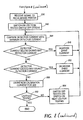
- Figure 8 is a flow chart describing the procedures used to readjust the calibration current after the printbar has been in use for a period of time. Blocks of the flowchart correspond to the initial set up of the system usually done during assembly of the printbar. Blocks of the flowchart correspond to recalibration of the printbar after a period of printing.
- the light output from a LED is detected at a photoreceptor plane.
- the light from the LED is compared to a desired reference light intensity in block 808.
- the reference light intensity is the same for all LEDs on the printbar. If the light output by the LED exceeds the reference light intensity, the current provided by the driver circuit is reduced in block 812. If the light output by the LED is less then the reference light intensity, the current provided by the driver circuit is increased in block 816.
- the calibration current provided by the driver circuit is stored in a memory location in block 820 for future reference. The driver current stored in the memory location is the maximum current provided by the driver circuit to the LED.
- the output of a photodetector typically a detector match current, is also recorded. The detector match current is the output of the photodetector when the LED outputs the reference light intensity at the photoreceptor plane.
- the printbar is installed inside the printer.
- the printbar is subject to normal use in block 832.
- Such normal use may include, but is not limited to receiving a signal from an imaging source such as a computer and causing the printbar to illuminate a media such that a charge distribution on the media matches the image from the imaging source.
- the charge distribution distributes a marking material over the substrate such that the marking material distribution matches the image from the imaging source.
- a signal is transmitted to recalibrate the printbar.
- a signal may be generated upon each power up of the printbar, or more typically, the signal may be generated after an extended period of printing.
- a signal to recalibrate the printbar is received, only one LED is switched on and all remaining LEDs are switched off in block 840.
- a comparison circuit compares the output of photodetector with the detector match current stored in memory in block 844.
- an ideal starting current is the calibration current for the LED, typically this calibration current was determined during printbar assembly or the last recalibration of the printbar.
- the drive circuit increases the current to the LED in block 848 to increase the LED output.
- the driver circuit decreases the drive current to the LED in block 852.
- the drive current used becomes the new calibration current for the LED.
- the new calibration current value replaces the calibration current value stored in memory.
- block 860 it is determined if this is the last LED to be tested in the printbar. When it is not the last LED to be tested, the tested LED is turned off, and the next LED to be tested in the printbar is turned on in box 864. The procedure beginning with box 844 is then repeated with a corresponding photodetector for the next LED to be tested. The procedure continues until every LED in the printbar has been tested. In the event that the LEDs have reached a point that regardless of drive current, the LED cannot output signal sufficient to cause the photodetector to output sufficient current, a warning may be provided to the user that the printbar should be replaced. In order to facilitate understanding of the invention, a number of details have been provided.
Landscapes
- Physics & Mathematics (AREA)
- Optics & Photonics (AREA)
- Engineering & Computer Science (AREA)
- General Engineering & Computer Science (AREA)
- General Physics & Mathematics (AREA)
- Theoretical Computer Science (AREA)
- Health & Medical Sciences (AREA)
- General Health & Medical Sciences (AREA)
- Toxicology (AREA)
- Printers Or Recording Devices Using Electromagnetic And Radiation Means (AREA)
- Facsimile Heads (AREA)
- Led Device Packages (AREA)
- Led Devices (AREA)
- Facsimile Scanning Arrangements (AREA)
- Fax Reproducing Arrangements (AREA)
Abstract
Description
- Printbars are used in printer systems to identify regions on a paper in which a marking material, such as a toner, is to be deposited. Modern printers often use an array of LEDs on a printbar to mark areas on which to deposit the toner. Each area identified by an LED corresponds to a "pixel" of deposited toner. For an ideal printed image, these pixels should be of uniform in size.
- In order to ensure uniformity of the pixels on a printed material, it is important that each LED on a printbar outputs an intensity that is similar to other LEDs on the printbar. During assembly, the LED printbars are corrected for non-uniformities between different LEDs in the printbar. However, almost immediately after being set in the factor, each LED in the printbar starts aging at a different rate. The different rates of aging and other changes to the LEDs and the drive systems results in a slow deterioration of printer output as non-uniformities increases in time causing more uneven print results. When non-uniformities reach an unacceptable level, service personnel are typically called to replace the printbar.
- A sy stem, incorporated into a printer, to monitor the LED printbar and automatically correct for deterioration of the LEDs is described. The system includes at least one detector integrated into the printer to detect the output intensity of each LED in the printbar. Each LED output is compared to a reference output. When a LED output varies from the reference by more than a predetermined amount, a power supply that provides power to the LED is adjusted to cause the LED to output the referenced intensity.
-
- Figure 1 shows a printer system including a printbar, that provides a system to monitor the output of the printbar.
- Figure 2 shows one embodiment of a cross section of a LED printbar including an illumination detection mechanism.
- Figure 3 shows an arrangement where each photodetector corresponds to a LED chip including multiple LEDs,
- Figure 4 shows an arrangement where a single strip photodetector is used in place of multiple discrete photodetectors.
- Figure 5 shows an arrangement an arrangement where the photodetector is mounted on a circuit board upon which the LED is mounted.
- Figure 6 shows the use of multiple photodetectors mounted as illustrated in Figure 5.
- Figure 7 shows the use of a single strip photodetector mounted on a circuit board upon which the LED is mounted.
- Figure 8 is a flow chart that describes that describes the method of detecting and adjusting power in a LED printbar.
-
- Figure 1 shows a
printbar 104 as used in aprinter system 100. The printbar receives a signal from a source of images, such as acomputer 108. The printbar is moved over aphotoreceptor plane 112 that receives the light output of the printbar and generated an electrical charge at each point that receives light from an LED. The output of the LEDs is adjusted to such that the light output of the printbar corresponds to a line of an image. As the printbar moves over the photoreceptor plane, a charge pattern is created on the photoreceptors that corresponds to the image to be printed. - After generation of a charge pattern on
photoreceptor plane 112, a markingmaterial source 116 deposits a marking material such as a toner over thephotoreceptor plane 112. The marking material adheres to the charged areas of the photoreceptor plane. Heat from aheat source 116 melts the marking material causing adhesion of the marking material tosubstrate 120, such as paper, that receives the marking material. (Pat, could you explain a little more how the charge pattern is transferred from the photoreceptors to the substrate upon which the toner is deposited?) - Figure 2 shows a cross section of one embodiment of
printbar 104. A plurality of integrated circuit (IC)driver chips 204 mounted on a printed circuit board 208 controls the output of a plurality ofLED chips 212. Aprintbar housing 216 andprintbar cover 220 support alens array 224.Lens array 224 is typically a Selfoc Lens array (SLA) that images thelight output 228 ofLED chips 212 onto photoreceptors in aphotoreceptor plane 232. The photoreceptors develop a charge according to the intensity of the light received from LED chips 21. The charge is transferred to a substrate to be marked. The charge attracts marking material deposited on the substrate to be marked. - Besides switching each LED on and off, driver circuits also control the individual drive current to each LED element. When initially fabricated, the drive current to each LED is adjusted to correct for non-uniform light output from the different LEDs in the printbar. The non-uniform outputs typically result from slight differences in LED parameters that occur during the fabrication process. For example some LEDs may have slightly thicker active regions than other LEDs. Before correction, these non-uniformities typically result in a 20 to 30% variation in light intensity output among different LED chips at a given current input. Even when differences in process parameters are minimized by forming different LEDs on the same chip, the different LEDs within the same chip typically still have a 5 to 10% variation in light intensity at a given input current.
- In printing applications, each LED typically corresponds to a pixel. The toner deposited per pixel is a function of the LED output corresponding to the pixel. Relatively minor variation of even 5 to 10% can result in a noticeable decline in print quality because the human eye is very sensitive to intensity differences over small distances.
- To correct for these variations, each driver circuit is also adjusted to correct for the variations. During final assembly on the production line, the output of each LED is measured at the SLA image plane. The output of the driver circuit is then adjusted to bring the light intensity output by each LED to a certain predetermined value within the illumination uniformity specification (typically within 1% to 2.5% of a desired intensity value). Thus a calibration current, the amount of drive current used to achieve the correct illumination level, is measured and stored.
- During fabrication of the LED printbar, the light that reaches a
detector 236 when a corresponding LED receives a corresponding calibration current is measured and recorded.Detector 236 is typically a photodetector that outputs a current, the current being a function of the number of photons (light intensity) above a certain wavelength that reaches the photodetector. A detector match current output bydetector 236 when the LED receives a calibration current that results in the detector outputting the desired intensity of light in the SLA image plane is stored in memory. The output ofdetector 236 will be used for adjustments to the LED in the field. - When printing an image, each LED may output different intensities that correspond to the different gray levels of a pixel being printed. The adjustment in intensity is achieved by scaling the driver circuit output current. The actual current received by the LED to print a pixel is thus a scaling of the calibrated current. For example, when a pixel darkness is 50% of the darkest printed pixel, a scaling factor of 50% is multiplied to the calibrated current corresponding to the LED. The scaling factor is the same for all LEDs, only the calibration current differs from pixel to pixel.
- As the printbar undergoes thermal changes and ages, the LED output at a given driver current usually declines. The rate of decline of different LEDs in the printbar is not uniform. In traditional systems, when the differing rates of decline result in output intensity differences between adjacent LEDs exceeding acceptable specifications, the LED printbar is replaced even though the LEDs may still have a significant period of useful life. A LED printbar can range in price from $100 to $2,000, thus replacing a LED printbar with significant potential remaining life is a large waste of resources. The invention avoids such replacement by periodically recalibrating the printbar using the stored photodetector outputs. The recalibration process using the photodetector is described in the flow chart and description accompanying Figure 8.
- Although Figure 2 shows a
single detector 236 corresponding to each LED, in order to save on fabrication costs, it is possible to implement the system of the present invention using fewer discrete photodetectors. Figure 3 shows using adiscrete photodetectors photodetector 300. Each LED chip such as LED chip 312 includes a plurality of LEDs such asLED - Alternate embodiments may be implemented that use one discrete photodetector for every two or more LED chips. However, reducing the number of discrete detectors increases the solid angle from which light will be received from associated LEDs because the LEDs will be spread over a wider area. The radiation pattern output by each LED may not be uniform in different directions, thus LEDs directly under the detector may provide more accurate reading relating to the decrease in output in the photoreceptor plane then LEDs located a significant distance off axis of the detector. Thus, when the number of photodetectors should be kept sufficient such that the detection of LED output occurs over a reasonable dynamic range.
- One method of avoiding the problem of discrete photodetectors located significantly off axis from the LED being detected is to utilize a strip photodetector as shown in Figure 4. In figure 4, a
strip photodetector 404 runs along theprintbar 408 parallel to the series of LEDs. The output of each LED can then be individually measured by keeping all LEDs off and switching only one LED on at a particular point in time. The output ofstrip photodetector 404 is then measured with the only one LED on. - Although, Figure 2 shows
photodetector 236 mounted directly to the cover of the printbar, alternate locations for the photodetector are also possible. The position on the cover is ideal for receiving light from the LED, however, fabrication may be simplified by mounting the detector on the circuit board as shown in Figure 5. - In Figure 5, a
driver circuit 504 mounted on printedcircuit board 508 provides power to aLED 512 onLED chip 516.Light 520 output fromLED 512 is focused by alens array 524 onto aphotoreceptor plane 528. However, significant light is also reflected fromprintbar cover 532 as well asprintbar housing 536. The reflected light is detected by aphotodetector 540 mounted on printedcircuit board 508. - Figure 6 shows the use of a plurality of
discrete photodetectors LED chips single strip photodetector 704 running parallel to a series ofLED chips - Figure 8 is a flow chart describing the procedures used to readjust the calibration current after the printbar has been in use for a period of time. Blocks of the flowchart correspond to the initial set up of the system usually done during assembly of the printbar. Blocks of the flowchart correspond to recalibration of the printbar after a period of printing.
- In
block 804, the light output from a LED is detected at a photoreceptor plane. The light from the LED is compared to a desired reference light intensity inblock 808. The reference light intensity is the same for all LEDs on the printbar. If the light output by the LED exceeds the reference light intensity, the current provided by the driver circuit is reduced inblock 812. If the light output by the LED is less then the reference light intensity, the current provided by the driver circuit is increased inblock 816. When the light output by the LED is within a specified tolerance of the reference light intensity at the photoreceptor, the calibration current provided by the driver circuit is stored in a memory location inblock 820 for future reference. The driver current stored in the memory location is the maximum current provided by the driver circuit to the LED. Inblock 824, the output of a photodetector, typically a detector match current, is also recorded. The detector match current is the output of the photodetector when the LED outputs the reference light intensity at the photoreceptor plane. - In
block 828, the printbar is installed inside the printer. The printbar is subject to normal use inblock 832. Such normal use may include, but is not limited to receiving a signal from an imaging source such as a computer and causing the printbar to illuminate a media such that a charge distribution on the media matches the image from the imaging source. The charge distribution distributes a marking material over the substrate such that the marking material distribution matches the image from the imaging source. - In
block 836, a signal is transmitted to recalibrate the printbar. Such a signal may be generated upon each power up of the printbar, or more typically, the signal may be generated after an extended period of printing. When a signal to recalibrate the printbar is received, only one LED is switched on and all remaining LEDs are switched off inblock 840. - In
block 844, a comparison circuit compares the output of photodetector with the detector match current stored in memory inblock 844. Typically, an ideal starting current is the calibration current for the LED, typically this calibration current was determined during printbar assembly or the last recalibration of the printbar. When the output of the photodetector is below the stored maximum detector current for the LED being tested, the drive circuit increases the current to the LED inblock 848 to increase the LED output. When the comparison circuit determines that the output of the photodetector exceeds the detector match current stored in memory, the driver circuit decreases the drive current to the LED inblock 852. When the comparison circuit determines that the output of the photodetector matches the stored detector match current value within a specified tolerance, the drive current used becomes the new calibration current for the LED. Inblock 856, the new calibration current value replaces the calibration current value stored in memory. - In
block 860, it is determined if this is the last LED to be tested in the printbar. When it is not the last LED to be tested, the tested LED is turned off, and the next LED to be tested in the printbar is turned on inbox 864. The procedure beginning withbox 844 is then repeated with a corresponding photodetector for the next LED to be tested. The procedure continues until every LED in the printbar has been tested. In the event that the LEDs have reached a point that regardless of drive current, the LED cannot output signal sufficient to cause the photodetector to output sufficient current, a warning may be provided to the user that the printbar should be replaced.
In order to facilitate understanding of the invention, a number of details have been provided. For example, various positioning of the intensity detectors, and even example materials that may be used to fabricate the intensity detectors have been recited. These details are provided to facilitate an understand of the invention and to provide example embodiments, but are not intended to limit the scope of the invention which should only be limited by the claims as given below.
Claims (8)
- An improved printbar comprising:a plurality of light emitting diodes to provide light to an imaging device;at least one photodetector to detect the power output of each LED in the plurality of LEDs; and,an adjustable power supply configured to allow individual adjustment of power provided to each LED in the plurality of LEDs, the power provided to the LED adjusted based on the feedback from the at least one photodetector.
- The improved printbar of claim 1 wherein the at least one photodetector is multiplexed in time to determine the output of a first LED in the plurality of LEDs at a first time and to determine the output of a second LED in the plurality of LEDs at a second time.
- The improved printbar of claim 1 wherein the improved printbar includes at least tow photodetectors.
- T he i mproved p rintbar of claim 3 w herein each p hotodetector corresponds to a LED chip .
- The improved printbar of claim 1 wherein the adjustable power supply changes the amount of current provided to the LED.
- The improved printbar of claim 1 further comprising:a storage device to store a calibration current for each LED, the calibration current being the current to be provided to the LED to cause the LED to output a predetermined intensity of light at a photoreceptor plane.
- A method of calibrating a printbar in a printer comprising the operations of:utilizing a printbar to output an image;determining when the printbar needs to be recalibrated;detecting at a photodetector integrated into said printer, the output of a Light emitting diode on the printbar and adjusting a current provided to the Light emitting diode until the intensity of light detected by the photodetector matches a reference intensity determined during assembly of the printbar.
- The method of claim 7 further comprising the operation of:replacing a reference current value stored in memory with a revised reference current value, the revised reference current value indicating the new current provided to the light emitting diode that causes the intensity of light detected by the photodetector to match the reference intensity determined during assembly of the printbar.
Applications Claiming Priority (2)
| Application Number | Priority Date | Filing Date | Title |
|---|---|---|---|
| US25484 | 2001-12-26 | ||
| US10/025,484 US6828538B2 (en) | 2001-12-26 | 2001-12-26 | Illumination detection method for LED printbars |
Publications (3)
| Publication Number | Publication Date |
|---|---|
| EP1326198A2 true EP1326198A2 (en) | 2003-07-09 |
| EP1326198A3 EP1326198A3 (en) | 2004-05-12 |
| EP1326198B1 EP1326198B1 (en) | 2014-02-26 |
Family
ID=21826344
Family Applications (1)
| Application Number | Title | Priority Date | Filing Date |
|---|---|---|---|
| EP02028810.6A Expired - Lifetime EP1326198B1 (en) | 2001-12-26 | 2002-12-23 | Illumination detection method and apparatus for led printbars |
Country Status (3)
| Country | Link |
|---|---|
| US (1) | US6828538B2 (en) |
| EP (1) | EP1326198B1 (en) |
| JP (1) | JP2003266791A (en) |
Cited By (2)
| Publication number | Priority date | Publication date | Assignee | Title |
|---|---|---|---|---|
| CN103995449A (en) * | 2013-02-20 | 2014-08-20 | 柯尼卡美能达株式会社 | Optical writing device and image forming apparatus |
| US10068165B2 (en) | 2013-04-12 | 2018-09-04 | Cardlab Aps | Card, an assembly, a method of assembling the card and a method of outputting information |
Families Citing this family (20)
| Publication number | Priority date | Publication date | Assignee | Title |
|---|---|---|---|---|
| JP2005519789A (en) * | 2002-03-12 | 2005-07-07 | ヒューレット−パッカード インディゴ ベスローテン フェンノートシャップ | Printing device with LED print head |
| US20050280694A1 (en) * | 2004-05-20 | 2005-12-22 | Seiko Epson Corporation | Line head and image forming apparatus incorporating the same |
| EP1598200A3 (en) * | 2004-05-21 | 2009-05-06 | Seiko Epson Corporation | Line head and image forming apparatus incorporating the same |
| US20060203078A1 (en) * | 2005-03-11 | 2006-09-14 | Naugler W E Jr | Feedback control apparatus and method for an emissive printhead |
| US7053920B1 (en) * | 2005-03-11 | 2006-05-30 | Nuelight Corporation | Feedback control apparatus and method for an emissive printhead |
| US7230222B2 (en) * | 2005-08-15 | 2007-06-12 | Avago Technologies Ecbu Ip (Singapore) Pte. Ltd. | Calibrated LED light module |
| US20070201231A1 (en) * | 2005-10-03 | 2007-08-30 | Infocus Corporation | System and method for resetting a light counter |
| JP2007261064A (en) * | 2006-03-28 | 2007-10-11 | Matsushita Electric Ind Co Ltd | Image forming apparatus |
| JP4877239B2 (en) * | 2006-03-28 | 2012-02-15 | パナソニック電工株式会社 | Method for manufacturing light emitting device |
| JP5010198B2 (en) * | 2006-07-26 | 2012-08-29 | パナソニック株式会社 | Light emitting device |
| JP5010199B2 (en) * | 2006-07-26 | 2012-08-29 | パナソニック株式会社 | Light emitting device |
| JP2009010045A (en) * | 2007-06-26 | 2009-01-15 | Panasonic Electric Works Co Ltd | Light emitting device |
| US8042910B2 (en) * | 2008-05-29 | 2011-10-25 | Hewlett-Packard Development Company, L.P. | Replaceable printbar assembly |
| US20100007588A1 (en) * | 2008-07-09 | 2010-01-14 | Adaptive Micro Systems Llc | System and method for led degradation and temperature compensation |
| JP4798249B2 (en) * | 2009-03-31 | 2011-10-19 | カシオ計算機株式会社 | Exposure apparatus, light amount correction method for exposure apparatus, and image forming apparatus |
| JP2012119589A (en) * | 2010-12-02 | 2012-06-21 | Canon Inc | Emission control device and control method |
| US8570543B2 (en) * | 2011-02-16 | 2013-10-29 | Xerox Corporation | Device and method for improving xerographic voltage uniformity for an image recording apparatus |
| WO2013159812A1 (en) | 2012-04-24 | 2013-10-31 | Hewlett-Packard Development Company, L.P. | Printing system and method of operation |
| TWI477404B (en) * | 2012-06-08 | 2015-03-21 | Nisho Image Tech Inc | Compensation and check method for light quantity of light-emitting device |
| JP7009856B2 (en) * | 2017-09-11 | 2022-01-26 | コニカミノルタ株式会社 | Optical writing device and image forming device equipped with it |
Family Cites Families (7)
| Publication number | Priority date | Publication date | Assignee | Title |
|---|---|---|---|---|
| US4588883A (en) | 1983-11-18 | 1986-05-13 | Eastman Kodak Company | Monolithic devices formed with an array of light emitting diodes and a detector |
| US4897672A (en) | 1987-07-02 | 1990-01-30 | Fujitsu Limited | Method and apparatus for detecting and compensating light emission from an LED array |
| GB8722944D0 (en) | 1987-09-30 | 1987-11-04 | Plessey Co Plc | Calibration system for led array |
| US5016027A (en) | 1989-12-04 | 1991-05-14 | Hewlett-Packard Company | Light output power monitor for a LED printhead |
| US5917534A (en) | 1995-06-29 | 1999-06-29 | Eastman Kodak Company | Light-emitting diode arrays with integrated photodetectors formed as a monolithic device and methods and apparatus for using same |
| JPH10243171A (en) * | 1997-02-25 | 1998-09-11 | Brother Ind Ltd | Image reading device |
| JP2000033731A (en) * | 1998-07-17 | 2000-02-02 | Citizen Watch Co Ltd | Calibration device of light emitting element in optical printer |
-
2001
- 2001-12-26 US US10/025,484 patent/US6828538B2/en not_active Expired - Fee Related
-
2002
- 2002-12-23 EP EP02028810.6A patent/EP1326198B1/en not_active Expired - Lifetime
- 2002-12-24 JP JP2002371339A patent/JP2003266791A/en active Pending
Non-Patent Citations (1)
| Title |
|---|
| None |
Cited By (4)
| Publication number | Priority date | Publication date | Assignee | Title |
|---|---|---|---|---|
| CN103995449A (en) * | 2013-02-20 | 2014-08-20 | 柯尼卡美能达株式会社 | Optical writing device and image forming apparatus |
| US9335652B2 (en) | 2013-02-20 | 2016-05-10 | Konica Minolta, Inc. | Optical writing device and image forming apparatus |
| CN103995449B (en) * | 2013-02-20 | 2016-09-21 | 柯尼卡美能达株式会社 | Optical writing device and image processing system |
| US10068165B2 (en) | 2013-04-12 | 2018-09-04 | Cardlab Aps | Card, an assembly, a method of assembling the card and a method of outputting information |
Also Published As
| Publication number | Publication date |
|---|---|
| US6828538B2 (en) | 2004-12-07 |
| US20030116694A1 (en) | 2003-06-26 |
| EP1326198A3 (en) | 2004-05-12 |
| EP1326198B1 (en) | 2014-02-26 |
| JP2003266791A (en) | 2003-09-24 |
Similar Documents
| Publication | Publication Date | Title |
|---|---|---|
| EP1326198B1 (en) | Illumination detection method and apparatus for led printbars | |
| EP0307994B1 (en) | An exposure device with an aging correction system for a led printer | |
| JPH0696294B2 (en) | Electrophotographic printing apparatus having exposure energy correction device for optical character generator | |
| US5016027A (en) | Light output power monitor for a LED printhead | |
| US5668587A (en) | Automatic LED printbar uniformity and adjustment | |
| US4857944A (en) | Recalibration system for LED array | |
| US7804513B2 (en) | Optical writing unit, image forming apparatus, process cartridge, and method of adjusting light intensity | |
| US20050174420A1 (en) | Method and apparatus for measuring forward voltage drop of light emitting element, light source apparatus, and thermal printer | |
| US7068295B2 (en) | Optical writing unit, a driving method thereof, and an image forming apparatus | |
| US4998118A (en) | LED printhead with post lens optical feedback and method of controlling same | |
| US6713754B1 (en) | Device and method for exposing visual data on light-sensitive recording material | |
| JP2003220728A (en) | Method for correcting exposure nonuniformity and led printing bar | |
| CN103488067A (en) | Light quantity compensation inspection method for light emitting device | |
| US8724082B2 (en) | Semiconductor laser driver and image forming apparatus incorporating same | |
| US7123278B2 (en) | Led printer and image forming apparatus including the same | |
| JP5217364B2 (en) | Reflection characteristic measuring device | |
| JP4816006B2 (en) | Print head and image forming apparatus | |
| JP2004148688A (en) | Optical printhead correction method, optical printhead, and image forming apparatus | |
| JP2004098390A (en) | Image forming apparatus | |
| JP2007182073A (en) | Adjusting method for exposure device for electronic photograph printer, and exposure device | |
| US7791629B2 (en) | Exposure device, printing apparatus employing an exposure device and method for adjusting a non-impact printing apparatus | |
| JP2008093835A (en) | Print head and image forming apparatus | |
| EP1607902B1 (en) | Adjustment of exposure power in a LED printer | |
| JP2006255976A (en) | Image forming device, and control method for printing head | |
| JP2005081701A (en) | Method for correcting quantity of light of led print head, and image forming apparatus employing it |
Legal Events
| Date | Code | Title | Description |
|---|---|---|---|
| PUAI | Public reference made under article 153(3) epc to a published international application that has entered the european phase |
Free format text: ORIGINAL CODE: 0009012 |
|
| AK | Designated contracting states |
Designated state(s): AT BE BG CH CY CZ DE DK EE ES FI FR GB GR IE IT LI LU MC NL PT SE SI SK TR |
|
| AX | Request for extension of the european patent |
Extension state: AL LT LV MK RO |
|
| PUAL | Search report despatched |
Free format text: ORIGINAL CODE: 0009013 |
|
| AK | Designated contracting states |
Kind code of ref document: A3 Designated state(s): AT BE BG CH CY CZ DE DK EE ES FI FR GB GR IE IT LI LU MC NL PT SE SI SK TR |
|
| AX | Request for extension of the european patent |
Extension state: AL LT LV MK RO |
|
| RIC1 | Information provided on ipc code assigned before grant |
Ipc: 7G 06K 15/12 A |
|
| 17P | Request for examination filed |
Effective date: 20041112 |
|
| AKX | Designation fees paid |
Designated state(s): DE FR GB |
|
| 17Q | First examination report despatched |
Effective date: 20050411 |
|
| GRAP | Despatch of communication of intention to grant a patent |
Free format text: ORIGINAL CODE: EPIDOSNIGR1 |
|
| INTG | Intention to grant announced |
Effective date: 20130712 |
|
| GRAS | Grant fee paid |
Free format text: ORIGINAL CODE: EPIDOSNIGR3 |
|
| GRAA | (expected) grant |
Free format text: ORIGINAL CODE: 0009210 |
|
| AK | Designated contracting states |
Kind code of ref document: B1 Designated state(s): DE FR GB |
|
| REG | Reference to a national code |
Ref country code: GB Ref legal event code: FG4D |
|
| REG | Reference to a national code |
Ref country code: DE Ref legal event code: R096 Ref document number: 60246008 Country of ref document: DE Effective date: 20140403 |
|
| REG | Reference to a national code |
Ref country code: DE Ref legal event code: R097 Ref document number: 60246008 Country of ref document: DE |
|
| PLBE | No opposition filed within time limit |
Free format text: ORIGINAL CODE: 0009261 |
|
| STAA | Information on the status of an ep patent application or granted ep patent |
Free format text: STATUS: NO OPPOSITION FILED WITHIN TIME LIMIT |
|
| 26N | No opposition filed |
Effective date: 20141127 |
|
| REG | Reference to a national code |
Ref country code: DE Ref legal event code: R097 Ref document number: 60246008 Country of ref document: DE Effective date: 20141127 |
|
| REG | Reference to a national code |
Ref country code: FR Ref legal event code: PLFP Year of fee payment: 14 |
|
| PGFP | Annual fee paid to national office [announced via postgrant information from national office to epo] |
Ref country code: DE Payment date: 20151119 Year of fee payment: 14 Ref country code: GB Payment date: 20151125 Year of fee payment: 14 |
|
| PGFP | Annual fee paid to national office [announced via postgrant information from national office to epo] |
Ref country code: FR Payment date: 20151123 Year of fee payment: 14 |
|
| REG | Reference to a national code |
Ref country code: DE Ref legal event code: R119 Ref document number: 60246008 Country of ref document: DE |
|
| GBPC | Gb: european patent ceased through non-payment of renewal fee |
Effective date: 20161223 |
|
| REG | Reference to a national code |
Ref country code: FR Ref legal event code: ST Effective date: 20170831 |
|
| PG25 | Lapsed in a contracting state [announced via postgrant information from national office to epo] |
Ref country code: FR Free format text: LAPSE BECAUSE OF NON-PAYMENT OF DUE FEES Effective date: 20170102 |
|
| PG25 | Lapsed in a contracting state [announced via postgrant information from national office to epo] |
Ref country code: DE Free format text: LAPSE BECAUSE OF NON-PAYMENT OF DUE FEES Effective date: 20170701 Ref country code: GB Free format text: LAPSE BECAUSE OF NON-PAYMENT OF DUE FEES Effective date: 20161223 |