EP1326081A2 - Zero-cross detection circuit - Google Patents
Zero-cross detection circuit Download PDFInfo
- Publication number
- EP1326081A2 EP1326081A2 EP02028867A EP02028867A EP1326081A2 EP 1326081 A2 EP1326081 A2 EP 1326081A2 EP 02028867 A EP02028867 A EP 02028867A EP 02028867 A EP02028867 A EP 02028867A EP 1326081 A2 EP1326081 A2 EP 1326081A2
- Authority
- EP
- European Patent Office
- Prior art keywords
- zero
- cross detection
- transistor
- detection circuit
- power supply
- Prior art date
- Legal status (The legal status is an assumption and is not a legal conclusion. Google has not performed a legal analysis and makes no representation as to the accuracy of the status listed.)
- Granted
Links
Images



Classifications
-
- H—ELECTRICITY
- H03—ELECTRONIC CIRCUITRY
- H03K—PULSE TECHNIQUE
- H03K5/00—Manipulating of pulses not covered by one of the other main groups of this subclass
- H03K5/153—Arrangements in which a pulse is delivered at the instant when a predetermined characteristic of an input signal is present or at a fixed time interval after this instant
- H03K5/1536—Zero-crossing detectors
-
- G—PHYSICS
- G01—MEASURING; TESTING
- G01R—MEASURING ELECTRIC VARIABLES; MEASURING MAGNETIC VARIABLES
- G01R19/00—Arrangements for measuring currents or voltages or for indicating presence or sign thereof
- G01R19/175—Indicating the instants of passage of current or voltage through a given value, e.g. passage through zero
-
- H—ELECTRICITY
- H02—GENERATION; CONVERSION OR DISTRIBUTION OF ELECTRIC POWER
- H02M—APPARATUS FOR CONVERSION BETWEEN AC AND AC, BETWEEN AC AND DC, OR BETWEEN DC AND DC, AND FOR USE WITH MAINS OR SIMILAR POWER SUPPLY SYSTEMS; CONVERSION OF DC OR AC INPUT POWER INTO SURGE OUTPUT POWER; CONTROL OR REGULATION THEREOF
- H02M1/00—Details of apparatus for conversion
- H02M1/08—Circuits specially adapted for the generation of control voltages for semiconductor devices incorporated in static converters
- H02M1/083—Circuits specially adapted for the generation of control voltages for semiconductor devices incorporated in static converters for the ignition at the zero crossing of the voltage or the current
Definitions
- the present invention relates to a zero-cross detection circuit for detecting a point at which an input alternating-current (AC) voltage crosses a predetermined voltage (0 V). More particularly, the present invention relates to a zero-cross detection circuit which is connected to a full-wave rectifying and smoothing circuit powered from a commercial AC power supply for full-wave rectification and smoothing, and which is also connected to a switching regulator for separating and stepping down the output from the full-wave rectifying and smoothing circuit to output a desired DC voltage.
- AC alternating-current
- Fig. 10 is a circuit diagram of a power supply circuit using a commercial AC power input, in particular, showing a zero-cross detection circuit in the related art for detecting a point at which an input AC voltage crosses zero volts, and a rectifying and smoothing circuit and a switching regulator which are connected to the zero-cross detection circuit.
- lines Line1 and Line2 are connected to a commercial AC power supply through a filter circuit (not shown).
- the full-wave rectifying and smoothing circuit is formed of diodes D11, D12, D13, and D14, and a smoothing capacitor C11.
- the switching regulator which is the self-excitation type is formed of components indicated by Q21, Q22, C21, C22, C31, C32, D31, IC31, R21 to R27, R31 to R35, and PC21.
- the switching regulator is insulated by a transformer T21, and generates a constant voltage of +24 V.
- the zero-cross detection circuit is formed of components indicated by Q41, C41, C42, D41, R41, R43, R44, R45, and PC41.
- a low-voltage output terminal of the full-wave rectifying and smoothing circuit is connected to the emitter of the n-p-n transistor Q41, and the resistor R43 is connected between the base and emitter of the transistor Q41.
- the resistor R43 and the capacitor C41 are connected in parallel with each other, and the resistor R41 is connected between the capacitor C41 and the line Line1.
- a half-wave rectifying circuit is formed of the resistors R41 and R43 in the zero-cross detection circuit, and the diode D13, and the output of the half-wave rectifying circuit is applied between the base and emitter of the transistor Q41. If the potential of the line Line1 is higher than the potential of the line Line2, a current flows in the resistor R41; otherwise, no current flows in the resistor R41.
- the resistances of the resistors R41 and R43 are set to suitable values so that the collector potential in the transistor Q41 can substantially change according to the potential magnitude of the lines Line1 and Line2.
- the high/low edges of the collector potential in the transistor Q41 correspond to zero crossings, and a zero-cross signal ZEROX is transmitted to the secondary of the transformer T21 via the photocoupler PC41.
- the capacitor C41 is a capacitor for removing noise, and is not essential to the zero-cross detection circuit.
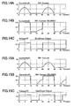
- Figs. 11A to 11C and 12A to 12C are signal waveforms of the components in the zero-cross detection circuit.
- Figs. 11A to 11C and 12A to 12C the x-axis represents time.
- Fig. 11A shows the potential of the line Line1 with respect to a ground GND
- Fig. 11B shows the potential of the line Line2 with respect to the ground GND
- Fig. 11C shows the difference in potential between the lines Line1 and Line2.
- Fig. 12A shows a current flowing in the resistor R41
- Fig. 12B shows an enlarged version of the y-axis in Fig. 12A
- Fig. 12C shows the phototransistor collector potential in the secondary of the photocoupler PC41, that is, the zero-cross signal ZEROX.
- the voltage is stepped down from the output (+24 V) of the switching regulator to +3.3 V.
- Fig. 13 shows another zero-cross detection circuit in the related art.
- the zero-cross detection circuits shown in Figs. 10 and 13 are different from each other in that the zero-cross detection circuit shown in Fig. 13 further includes capacitors C12 and C13.
- the capacitors C12 and C13 are connected to the high-voltage output terminal and the low-voltage output terminal of the full-wave rectifying and smoothing circuit, respectively, and the node between the capacitors C12 and C13 is grounded.
- a capacitor (a so-called Y-capacitor) of approximately several thousand picofarads is connected between a commercial AC power supply line and a ground GND.
- the capacitors C12 and C13 are Y-capacitors.
- a Y-capacitor may be connected to an input terminal of a full-wave rectifying circuit, it is more effective for the terminal noise suppression purpose to connect a Y-capacitor to an output terminal of a full-wave rectifying circuit.
- the configuration shown in Fig. 13 is often used.
- Figs. 14A to 14C are signal waveforms of the components in the zero-cross detection circuit when the Y-capacitors in the circuit shown in Fig. 13 have a relatively small capacitance. Since the waveforms indicating the potential of the line Line1 with respect to the ground GND, the potential of the line Line2 with respect to the ground GND, and the difference in potential between the lines Line1 and Line2 are the same as those shown in Figs. 11A to 11C, a description thereof is omitted.
- Fig. 14A shows a current flowing in the resistor R41
- Fig. 14B shows an enlarged version of the y-axis in Fig. 14A
- Fig. 14C shows the phototransistor collector potential in the secondary of the photocoupler PC41, that is, the zero-cross signal ZEROX.
- a zero-cross signal ZEROX can be successfully generated.
- Figs. 15A to 15C are signal waveforms of the components in the zero-cross detection circuit when the Y-capacitors in the circuit shown in Fig. 13 have a relatively large capacitance. Since the waveforms indicating the potential of the line Line1 with respect to the ground GND, the potential of the line Line2 with respect to the ground GND, and the difference in potential between the lines Line1 and Line2 are the same as those shown in Figs. 11A to 11C, a description thereof is omitted.
- Fig. 15A shows a current flowing in the resistor R41
- Fig. 15B shows an enlarged version of the y-axis in Fig. 15A
- Fig. 15C shows the phototransistor collector potential in the secondary of the photocoupler PC41, that is, the zero-cross signal ZEROX.
- Figs. 15A to 15C if the Y-capacitors have a large capacitance, the zero-cross signal ZEROX shown in Fig. 15C does not indicate a correct zero-cross point.
- This current flows in the Y-capacitors C12 and C13 towards the ground GND.
- the potential of either the line Line1 or Line2, whichever is lower, is used as the low-voltage output potential of the full-wave rectifying and smoothing circuit with respect to the ground GND. This exhibits a half-wave rectified waveform.
- the high-voltage output potential of the full-wave rectifying and smoothing circuit with respect to the ground GND is produced by adding the capacitance potential stored in the capacitor C11 to the low-voltage output potential, and, if a DC component is removed, the output would be equal to the half-wave rectified waveform.
- a current flowing in the Y-capacitors C12 and C13 is therefore produced by differentiating the voltage of the half-wave rectified waveform.
- This current flows in the rectifier diodes D11 to D14 when those diodes are conducting, and otherwise flows in the resistor R41. Since the full-wave rectifying and smoothing circuit is capacitor-input, the rectifier diodes D11 to D14 have a small conduction angle and do not conduct most of the time.
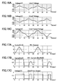
- Figs. 16A to 16C and 17A to 17C are signal waveforms of the components in the zero-cross detection circuit when the commercial AC power supply on which the third harmonic is superposed exhibits an undesirable waveform in the circuit shown in Fig. 13.
- Fig. 16A shows the potential of the line Line1 with respect to the ground GND
- Fig. 16B shows the potential of the line Line2 with respect to the ground GND
- Fig. 16C shows the difference in potential between the lines Line1 and Line2.
- Fig. 17A shows a current flowing in the resistor R41
- Fig. 17B shows an enlarged version of the y-axis in Fig. 17A
- Fig. 17C shows the phototransistor collector potential in the secondary of the photocoupler PC41, that is, the zero-cross signal ZEROX.
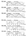
- Figs. 18A to 18C and 19A to 19C are signal waveforms of the components in the zero-cross detection circuit when the commercial AC power supply which has a 60° phase difference rather than a 180° phase difference exhibits an undesirable waveform in the circuit shown in Fig. 13.
- Fig. 18A shows the potential of the line Line1 with respect to the ground GND
- Fig. 18B shows the potential of the line Line2 with respect to the ground GND
- Fig. 18C shows the difference in potential between the lines Line1 and Line2.
- Fig. 19A shows a current flowing in the resistor R41
- Fig. 19B shows an enlarged version of the y-axis in Fig. 19A
- Fig. 19C shows the phototransistor collector potential in the secondary of the photocoupler PC41, that is, the zero-cross signal ZEROX.
- the harmonic component is also superposed on the output potential of the full-wave rectifying and smoothing circuit with respect to the ground GND.
- the harmonic distortion causes a current shown as the waveform between 15 and 20 msec in Fig. 17B to flow in the resistor R41.
- the difference in potential between the lines Line1 and Line2 is phase-shifted with respect to the output potential of the full-wave rectifying and smoothing circuit with respect to the ground GND, thus causing a current shown as the waveform between about 15 and 20 msec in Fig. 19B to flow in the resistor R41.
- the current flowing in the resistor R41 is zero at about 18 msec because the rectifier diodes D11 and D14 are conducting, and the current at this time is supplied to the Y-capacitors C11 and C12 via the diode D14.
- a zero-cross detection circuit is connected to a power supply device which includes a full-wave rectifying and smoothing circuit, two capacitors, and a switching regulator.
- the full-wave rectifying and smoothing circuit is powered via first and second lines from a commercial AC power supply for full-wave rectification and smoothing.
- the two capacitors have first ends connected to high-voltage and low-voltage output terminals of the full-wave rectifying and smoothing circuit, respectively, and second ends connected to a ground.
- the switching regulator separates and steps down the output from the full-wave rectifying and smoothing circuit to output a desired DC voltage.
- the zero-cross detection circuit includes a transistor of which the emitter is connected to the low-voltage output terminal of the full-wave rectifying and smoothing circuit for outputting a zero-cross detection signal from the collector; a first resistor connected between the base and emitter of the transistor; a second resistor connected between the first line and the base of the transistor; and a third resistor connected between the second line and the emitter of the transistor.
- the third resistor has substantially the same resistance as that of the second resistor.
- the zero-cross detection circuit according to the present invention can be correctly operated when the above-noted Y-capacitors are provided after a full-wave rectifying and smoothing circuit for the terminal noise suppression purpose. Furthermore, if the commercial AC power supply exhibits an undesirable waveform, the zero-cross detection circuit can reliably generate a zero-cross signal.
- the zero-cross detection circuit includes a diode connected between the base and emitter of the transistor in such a manner that the anode of the diode is connected to the emitter of the transistor.
- a diode may be connected between the first line and the second resistor in such a manner that the anode of the diode is connected to the first line.
- the second resistor and the diode may be replaced.
- Another diode may be connected between the second line and the third resistor in such a manner that the anode of the second diode is connected to the second line.
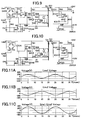
- Fig. 1 is a circuit diagram of a power supply device using a commercial AC power supply, showing a zero-cross circuit according to a first embodiment of the present invention, and a rectifying and smoothing circuit and a switching regulator which are connected to the zero-cross detection circuit.
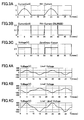
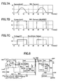
- Figs. 2A to 2C are waveforms of a normal commercial AC power supply.
- Figs. 3A to 3C are signal waveforms of the components in the zero-cross detection circuit shown in Fig. 1 when the Y-capacitors have a large capacitance.
- Figs. 4A to 4C are waveforms of an undesired commercial AC power supply which involves a third harmonic component.
- Figs. 5A to 5C are signal waveforms of the components in the zero-cross detection circuit shown in Fig. 1 when the third harmonic is superposed on the commercial AC power supply.
- Figs. 6A to 6C are waveforms of an undesired commercial AC power supply which has a 60° phase difference.
- Figs. 7A to 7C are signal waveforms of the components in the zero-cross detection circuit shown in Fig. 1 when the commercial AC power supply has a 60° phase difference.
- Fig. 8 is a circuit diagram of a power supply device including a zero-cross detection circuit according to a second embodiment of the present invention.
- Fig. 9 is a circuit diagram of a power supply device including a zero-cross detection circuit according to a third embodiment of the present invention.
- Fig. 10 is a circuit diagram of a power supply device using a commercial AC power input, showing a zero-cross detection circuit in the related art, and a rectifying and smoothing circuit and a switching regulator which are connected to the zero-cross detection circuit.
- Figs. 11A to 11C are waveforms of a normal AC power supply.
- Figs. 12A to 12C are signal waveforms of the components in the zero-cross detection circuit shown in Fig. 10.
- Fig. 13 is a circuit diagram of another zero-cross detection circuit in the related art.
- Figs. 14A to 14C are signal waveforms of components in the zero-cross detection circuit shown in Fig. 13 when Y-capacitors have a relatively small capacitance.
- Figs. 15A to 15C are signal waveforms of the components in the zero-cross detection circuit shown in Fig. 13 when the Y-capacitors have a relatively large capacitance.
- Figs. 16A to 16C are waveforms of an undesired commercial AC power supply which involves a third harmonic component.
- Figs. 17A to 17C are signal waveforms of the components in the zero-cross detection circuit shown in Fig. 13 when the commercial AC power supply on which the third harmonic is superposed exhibits an undesirable waveform.
- Figs. 18A to 18C are waveforms of an undesired commercial AC power supply which has a 60° phase difference.
- Figs. 19A to 19C are signal waveforms of the components in the zero-cross detection circuit shown in Fig. 13 when the commercial AC power supply which has a 60° phase difference exhibits an undesirable waveform.
- Fig. 1 is a circuit diagram of a power supply device including a zero-cross detection circuit according to a first embodiment of the present invention.
- the power supply device includes a zero-cross detection circuit, a rectifying and smoothing circuit, and a switching regulator, as in the circuit configuration shown in Fig. 13.
- the switching regulator of the self-excitation type is formed of components indicated by Q21, Q22, C21, C22, C31, C32, D31, IC31, R21 to R27, R31 to R35, and PC21.
- the zero-cross detection circuit is formed of components indicated by Q41, C41, C42, D41, R41 to R45, and PC41.
- the switching regulator includes a transformer T21 for separating and stepping down the DC output from the full-wave rectifying and smoothing circuit to output a desired DC voltage.
- the zero-cross detection circuit according to the present invention is different from that shown in Fig. 13 in that a resistor R42 is connected between the line Line2 and the low-voltage output terminal of the full-wave rectifying and smoothing circuit, i.e., the emitter of the transistor Q41.
- the resistor R42 allows a current to flow, and therefore allows a current flowing in the Y-capacitors (capacitors C12 and C13) to flow to the resistor R42. This hinders an unwanted current caused by the Y-capacitors from flowing to the resistor R41. Therefore, when the Y-capacitors have a large capacitance or when the commercial AC power supply exhibits an undesirable waveform, a zero-cross signal can be reliably generated.
- the resistor R42 is provided in a circuit portion which is an input to the zero-cross detection circuit from the line Line2. This allows an unwanted current caused by the Y-capacitors to bypass the zero-cross detection circuit, thereby reliably generating a zero-cross signal in the zero-cross detection circuit.
- the resistors R41 and R42 have substantially the same resistance in view of the following two points:
- Figs. 2A to 2C and 3A to 3C are signal waveforms of the components in the zero-cross detection circuit shown in Fig. 1 when the Y-capacitors have a large capacitance.
- Figs. 2A to 2C and 3A to 3C the x-axis represents time.
- Fig. 2A shows the potential of the line Line1 with respect to a ground GND
- Fig. 2B shows the potential of the line Line2 with respect to the ground GND
- Fig. 2C shows the difference in potential between the lines Line1 and Line2.
- Fig. 3A shows a current flowing in the resistor R41
- Fig. 3B shows an enlarged version of the y-axis in Fig. 3A
- Fig. 3C shows the phototransistor collector potential in the secondary of the photocoupler PC41, that is, the zero-cross signal ZEROX.
- Figs. 4A to 4C and 5A to 5C are signal waveforms of the components in the zero-cross detection circuit shown in Fig. 1 when the third harmonic is superposed on the commercial AC power supply.
- Figs. 6A to 6C and 7A to 7C are signal waveforms of the components in the zero-cross detection circuit shown in Fig. 1 when the commercial AC power supply has a 60° phase difference.
- a current flowing in the resistor R41 does not exhibit an undesirable waveform, thus allowing a correct zero-cross signal ZEROX to be generated, as shown in Figs. 3C, 5C, and 7C.
- Fig. 8 is a circuit diagram of a power supply device including a zero-cross detection circuit according to a second embodiment of the present invention.
- the second embodiment has substantially the same basic structure as the first embodiment, but includes a diode D42 connected between the base and emitter of the transistor Q41 in such a manner that the anode of the diode D42 is connected to the emitter of the transistor Q41.
- the diode D42 prevents a reverse bias from being applied between the base and emitter of the transistor Q41 if noise is present in the commercial AC power supply.
- Fig. 9 is a circuit diagram of a power supply device including a zero-cross detection circuit according to a third embodiment of the present invention.
- the third embodiment has substantially the same basic structure as the first embodiment, but includes a diode D43 connected in series with the resistor R41 in such a manner that the anode of the diode D43 is connected to the line Line1.
- the diode D43 also prevents a reverse bias from being applied between the base and emitter of the transistor Q41 if noise is caused in the commercial AC power supply.
- a diode which is the same as the diode D43 may be further connected between the line Line2 and the resistor R42 in such a manner that the anode of the additional diode is connected to the line Line2, thus making the resistors R41 and R42 symmetric.
- a zero-cross detection circuit includes a transistor of which the emitter is connected to the low-voltage output terminal of the full-wave rectifying and smoothing circuit for outputting a zero-cross detection signal from the collector; a first resistor is connected between the base and emitter of the transistor; a second resistor is connected between one of the power supply lines and the base of the transistor; and a third resistor is connected between the other power supply line and the emitter of the transistor.
Landscapes
- Physics & Mathematics (AREA)
- Engineering & Computer Science (AREA)
- Power Engineering (AREA)
- General Physics & Mathematics (AREA)
- Nonlinear Science (AREA)
- Measurement Of Current Or Voltage (AREA)
- Dc-Dc Converters (AREA)
Abstract
Description
The configuration shown in Fig. 13 is often used.
A current flowing in the Y-capacitors C12 and C13 is therefore produced by differentiating the voltage of the half-wave rectified waveform.
Claims (6)
- A zero-cross detection circuit connected to a power supply device, the power supply device including:said zero-cross detection circuit comprising:a full-wave rectifying and smoothing circuit powered via first and second lines from a commercial AC power supply for full-wave rectification and smoothing;two capacitors having first ends connected to a high-voltage output terminal and a low-voltage output terminal of the full-wave rectifying and smoothing circuit, respectively, and second ends connected to a ground; anda switching regulator for separating and stepping down the output from the full-wave rectifying and smoothing circuit to output a desired DC voltage,a transistor, having an emitter, a base, and a collector, of which the emitter is connected to the low-voltage output terminal of the full-wave rectifying and smoothing circuit for outputting a zero-cross detection signal from the collector;a first resistor connected between the base and emitter of the transistor;a second resistor connected between the first line and the base of the transistor; anda third resistor connected between the second line and the emitter of the transistor.
- A zero-cross detection circuit according to claim 1, wherein the third resistor has substantially the same resistance as that of the second resistor.
- A zero-cross detection circuit according to claim 1, further comprising a diode, having an anode and a cathode, connected between the base and emitter of the transistor in such a manner that the anode of the diode is connected to the emitter of the transistor.
- A zero-cross detection circuit according to claim 1, further comprising a diode, having an anode and a cathode, connected in series with the second resistor in such a manner that the anode of the diode is connected closer to the first line than to the transistor.
- A zero-cross detection circuit according to claim 4, further comprising a second diode, having an anode and a cathode, connected in series with the third resistor in such a manner that the anode of the second diode is connected closer to the second line than to the transistor.
- A zero-cross detection circuit according to claim 1, wherein the transistor is an n-p-n transistor.
Applications Claiming Priority (2)
| Application Number | Priority Date | Filing Date | Title |
|---|---|---|---|
| JP2001400778A JP3728245B2 (en) | 2001-12-28 | 2001-12-28 | Zero cross detection circuit |
| JP2001400778 | 2001-12-28 |
Publications (3)
| Publication Number | Publication Date |
|---|---|
| EP1326081A2 true EP1326081A2 (en) | 2003-07-09 |
| EP1326081A3 EP1326081A3 (en) | 2008-12-10 |
| EP1326081B1 EP1326081B1 (en) | 2010-10-06 |
Family
ID=19189673
Family Applications (1)
| Application Number | Title | Priority Date | Filing Date |
|---|---|---|---|
| EP02028867A Expired - Lifetime EP1326081B1 (en) | 2001-12-28 | 2002-12-23 | Zero-cross detection circuit |
Country Status (5)
| Country | Link |
|---|---|
| US (1) | US6664817B2 (en) |
| EP (1) | EP1326081B1 (en) |
| JP (1) | JP3728245B2 (en) |
| CN (1) | CN1248401C (en) |
| DE (1) | DE60237873D1 (en) |
Cited By (1)
| Publication number | Priority date | Publication date | Assignee | Title |
|---|---|---|---|---|
| US20140028354A1 (en) * | 2012-04-18 | 2014-01-30 | Huawei Technologies Co., Ltd. | Zero-crossing detection method and circuit |
Families Citing this family (13)
| Publication number | Priority date | Publication date | Assignee | Title |
|---|---|---|---|---|
| FR2873243A1 (en) * | 2004-07-13 | 2006-01-20 | St Microelectronics Sa | ADAPTABLE POWER CIRCUIT |
| EP1645885A1 (en) * | 2004-10-08 | 2006-04-12 | Abb Research Ltd. | Method for the determination of current zero crossing in an inverter |
| CA2623061A1 (en) * | 2007-03-02 | 2008-09-02 | Sean C. Carroll | Zero crossing circuit |
| JP5203643B2 (en) * | 2007-07-04 | 2013-06-05 | キヤノン株式会社 | Zero cross detection circuit, zero cross signal output circuit and power supply |
| JP5497751B2 (en) * | 2008-05-23 | 2014-05-21 | フィッシャー コントロールズ インターナショナル エルエルシー | Optical isolator multi-voltage detection circuit |
| KR101445842B1 (en) | 2008-05-29 | 2014-10-01 | 페어차일드코리아반도체 주식회사 | Converter |
| JP2010050820A (en) * | 2008-08-22 | 2010-03-04 | Oki Data Corp | Zero cross detection device and image forming apparatus |
| JP5932321B2 (en) * | 2011-12-12 | 2016-06-08 | キヤノン株式会社 | Power supply having zero cross detection circuit and image forming apparatus |
| JP5984404B2 (en) * | 2012-01-31 | 2016-09-06 | キヤノン株式会社 | Power supply and power failure detection device |
| EP2624422B1 (en) | 2012-01-31 | 2019-08-28 | Canon Kabushiki Kaisha | Power source, power failure detection apparatus, and image forming apparatus |
| TWI569563B (en) * | 2015-10-22 | 2017-02-01 | Multifunction Power Converter | |
| CN114924113B (en) * | 2022-04-02 | 2025-05-16 | 上海南芯半导体科技股份有限公司 | An inductor current zero-crossing detection device for a switching power supply |
| CN117478140B (en) * | 2023-12-26 | 2024-03-15 | 四川莱福德科技有限公司 | High-precision full-voltage alternating current-direct current sampling circuit and method for LED power supply |
Family Cites Families (6)
| Publication number | Priority date | Publication date | Assignee | Title |
|---|---|---|---|---|
| JPS5953673B2 (en) * | 1977-08-09 | 1984-12-26 | ソニー株式会社 | power circuit |
| JPS598430A (en) * | 1982-07-05 | 1984-01-17 | Nec Corp | Zero cross control circuit |
| JPH0656946B2 (en) * | 1984-06-26 | 1994-07-27 | 富士ゼロックス株式会社 | Zero Volt Detection Signal Generation Circuit in Zero Volt Switching Circuit |
| US5218509A (en) * | 1986-05-30 | 1993-06-08 | Robertshaw Controls Company | Electrically operated control device and system for an appliance and method of operating the same |
| JPH10333490A (en) * | 1997-05-30 | 1998-12-18 | Canon Inc | Image forming apparatus and power control method |
| US6272025B1 (en) * | 1999-10-01 | 2001-08-07 | Online Power Supply, Inc. | Individual for distributed non-saturated magnetic element(s) (referenced herein as NSME) power converters |
-
2001
- 2001-12-28 JP JP2001400778A patent/JP3728245B2/en not_active Expired - Fee Related
-
2002
- 2002-12-20 US US10/323,925 patent/US6664817B2/en not_active Expired - Lifetime
- 2002-12-23 DE DE60237873T patent/DE60237873D1/en not_active Expired - Lifetime
- 2002-12-23 EP EP02028867A patent/EP1326081B1/en not_active Expired - Lifetime
- 2002-12-25 CN CN02159558.5A patent/CN1248401C/en not_active Expired - Fee Related
Cited By (1)
| Publication number | Priority date | Publication date | Assignee | Title |
|---|---|---|---|---|
| US20140028354A1 (en) * | 2012-04-18 | 2014-01-30 | Huawei Technologies Co., Ltd. | Zero-crossing detection method and circuit |
Also Published As
| Publication number | Publication date |
|---|---|
| US6664817B2 (en) | 2003-12-16 |
| DE60237873D1 (en) | 2010-11-18 |
| CN1430064A (en) | 2003-07-16 |
| JP2003199343A (en) | 2003-07-11 |
| EP1326081A3 (en) | 2008-12-10 |
| JP3728245B2 (en) | 2005-12-21 |
| EP1326081B1 (en) | 2010-10-06 |
| US20030122591A1 (en) | 2003-07-03 |
| CN1248401C (en) | 2006-03-29 |
Similar Documents
| Publication | Publication Date | Title |
|---|---|---|
| EP1326081B1 (en) | Zero-cross detection circuit | |
| EP0715780B1 (en) | Bridge rectifier circuit having active switches and an active control circuit | |
| JP2002330589A (en) | Circuit that converts AC voltage to DC voltage | |
| CN102652391B (en) | Reverse recovery current prevention device, and motor driving device | |
| JP7379131B2 (en) | power converter | |
| US5740026A (en) | Controlled input circuit for an SCR to accept either AC or DC voltage | |
| JP2000116133A (en) | Waveform shaping circuit | |
| AU2004310594B2 (en) | Electric power converter apparatus | |
| JP3402031B2 (en) | DC power supply | |
| TWI239709B (en) | Rectifier circuit matched for power factor correction | |
| CN100525037C (en) | High voltage power generator | |
| EP0140418A1 (en) | Active double-sided rectifier circuit | |
| JP3417149B2 (en) | Power supply | |
| KR20000001444A (en) | SINGLE PHASE ACTIVE RECTIFIER FOR power FACTOR CONTROL | |
| JP2003235266A (en) | Three-phase full-wave rectifier | |
| JPH08214540A (en) | Power input circuit | |
| JPH06327148A (en) | Power supply circuit | |
| JP2001275358A (en) | Switching power supply | |
| JPH09308231A (en) | Switching power supply | |
| JPH04359674A (en) | DC power supply | |
| JPH07222447A (en) | Switching power supply | |
| KR900007132Y1 (en) | Converting circuit for power source | |
| JPS6146180A (en) | Rectified voltage multiplier circuit | |
| JP2016092929A (en) | Inverter circuit | |
| JPH09201055A (en) | Ac-dc voltage doubler rectifier circuit as well as adding circuit and or circuit using it |
Legal Events
| Date | Code | Title | Description |
|---|---|---|---|
| PUAI | Public reference made under article 153(3) epc to a published international application that has entered the european phase |
Free format text: ORIGINAL CODE: 0009012 |
|
| AK | Designated contracting states |
Designated state(s): AT BE BG CH CY CZ DE DK EE ES FI FR GB GR IE IT LI LU MC NL PT SE SI SK TR |
|
| AX | Request for extension of the european patent |
Extension state: AL LT LV MK RO |
|
| PUAL | Search report despatched |
Free format text: ORIGINAL CODE: 0009013 |
|
| AK | Designated contracting states |
Kind code of ref document: A3 Designated state(s): AT BE BG CH CY CZ DE DK EE ES FI FR GB GR IE IT LI LU MC NL PT SE SI SK TR |
|
| AX | Request for extension of the european patent |
Extension state: AL LT LV MK RO |
|
| RIC1 | Information provided on ipc code assigned before grant |
Ipc: H03K 5/1536 20060101ALI20081031BHEP Ipc: H02M 1/08 20060101ALI20081031BHEP Ipc: G01R 19/175 20060101AFI20030404BHEP |
|
| 17P | Request for examination filed |
Effective date: 20090610 |
|
| AKX | Designation fees paid |
Designated state(s): DE FR GB |
|
| GRAP | Despatch of communication of intention to grant a patent |
Free format text: ORIGINAL CODE: EPIDOSNIGR1 |
|
| GRAS | Grant fee paid |
Free format text: ORIGINAL CODE: EPIDOSNIGR3 |
|
| GRAA | (expected) grant |
Free format text: ORIGINAL CODE: 0009210 |
|
| AK | Designated contracting states |
Kind code of ref document: B1 Designated state(s): DE FR GB |
|
| REG | Reference to a national code |
Ref country code: GB Ref legal event code: FG4D |
|
| REF | Corresponds to: |
Ref document number: 60237873 Country of ref document: DE Date of ref document: 20101118 Kind code of ref document: P |
|
| PLBE | No opposition filed within time limit |
Free format text: ORIGINAL CODE: 0009261 |
|
| STAA | Information on the status of an ep patent application or granted ep patent |
Free format text: STATUS: NO OPPOSITION FILED WITHIN TIME LIMIT |
|
| 26N | No opposition filed |
Effective date: 20110707 |
|
| REG | Reference to a national code |
Ref country code: DE Ref legal event code: R097 Ref document number: 60237873 Country of ref document: DE Effective date: 20110707 |
|
| PGFP | Annual fee paid to national office [announced via postgrant information from national office to epo] |
Ref country code: FR Payment date: 20120103 Year of fee payment: 10 |
|
| REG | Reference to a national code |
Ref country code: FR Ref legal event code: ST Effective date: 20130830 |
|
| PG25 | Lapsed in a contracting state [announced via postgrant information from national office to epo] |
Ref country code: FR Free format text: LAPSE BECAUSE OF NON-PAYMENT OF DUE FEES Effective date: 20130102 |
|
| PGFP | Annual fee paid to national office [announced via postgrant information from national office to epo] |
Ref country code: GB Payment date: 20181221 Year of fee payment: 17 |
|
| PGFP | Annual fee paid to national office [announced via postgrant information from national office to epo] |
Ref country code: DE Payment date: 20190228 Year of fee payment: 17 |
|
| REG | Reference to a national code |
Ref country code: DE Ref legal event code: R119 Ref document number: 60237873 Country of ref document: DE |
|
| GBPC | Gb: european patent ceased through non-payment of renewal fee |
Effective date: 20191223 |
|
| PG25 | Lapsed in a contracting state [announced via postgrant information from national office to epo] |
Ref country code: GB Free format text: LAPSE BECAUSE OF NON-PAYMENT OF DUE FEES Effective date: 20191223 Ref country code: DE Free format text: LAPSE BECAUSE OF NON-PAYMENT OF DUE FEES Effective date: 20200701 |