EP1324205A1 - Memory device - Google Patents
Memory device Download PDFInfo
- Publication number
- EP1324205A1 EP1324205A1 EP01974708A EP01974708A EP1324205A1 EP 1324205 A1 EP1324205 A1 EP 1324205A1 EP 01974708 A EP01974708 A EP 01974708A EP 01974708 A EP01974708 A EP 01974708A EP 1324205 A1 EP1324205 A1 EP 1324205A1
- Authority
- EP
- European Patent Office
- Prior art keywords
- data
- read
- memory
- area
- prohibited
- Prior art date
- Legal status (The legal status is an assumption and is not a legal conclusion. Google has not performed a legal analysis and makes no representation as to the accuracy of the status listed.)
- Withdrawn
Links
Images




Classifications
-
- G—PHYSICS
- G06—COMPUTING OR CALCULATING; COUNTING
- G06F—ELECTRIC DIGITAL DATA PROCESSING
- G06F12/00—Accessing, addressing or allocating within memory systems or architectures
- G06F12/14—Protection against unauthorised use of memory or access to memory
-
- G—PHYSICS
- G07—CHECKING-DEVICES
- G07F—COIN-FREED OR LIKE APPARATUS
- G07F7/00—Mechanisms actuated by objects other than coins to free or to actuate vending, hiring, coin or paper currency dispensing or refunding apparatus
- G07F7/08—Mechanisms actuated by objects other than coins to free or to actuate vending, hiring, coin or paper currency dispensing or refunding apparatus by coded identity card or credit card or other personal identification means
- G07F7/10—Mechanisms actuated by objects other than coins to free or to actuate vending, hiring, coin or paper currency dispensing or refunding apparatus by coded identity card or credit card or other personal identification means together with a coded signal, e.g. in the form of personal identification information, like personal identification number [PIN] or biometric data
- G07F7/1008—Active credit-cards provided with means to personalise their use, e.g. with PIN-introduction/comparison system
-
- G—PHYSICS
- G06—COMPUTING OR CALCULATING; COUNTING
- G06F—ELECTRIC DIGITAL DATA PROCESSING
- G06F12/00—Accessing, addressing or allocating within memory systems or architectures
- G06F12/14—Protection against unauthorised use of memory or access to memory
- G06F12/1416—Protection against unauthorised use of memory or access to memory by checking the object accessibility, e.g. type of access defined by the memory independently of subject rights
- G06F12/1425—Protection against unauthorised use of memory or access to memory by checking the object accessibility, e.g. type of access defined by the memory independently of subject rights the protection being physical, e.g. cell, word, block
- G06F12/1441—Protection against unauthorised use of memory or access to memory by checking the object accessibility, e.g. type of access defined by the memory independently of subject rights the protection being physical, e.g. cell, word, block for a range
-
- G—PHYSICS
- G06—COMPUTING OR CALCULATING; COUNTING
- G06F—ELECTRIC DIGITAL DATA PROCESSING
- G06F21/00—Security arrangements for protecting computers, components thereof, programs or data against unauthorised activity
- G06F21/70—Protecting specific internal or peripheral components, in which the protection of a component leads to protection of the entire computer
- G06F21/78—Protecting specific internal or peripheral components, in which the protection of a component leads to protection of the entire computer to assure secure storage of data
- G06F21/79—Protecting specific internal or peripheral components, in which the protection of a component leads to protection of the entire computer to assure secure storage of data in semiconductor storage media, e.g. directly-addressable memories
-
- G—PHYSICS
- G06—COMPUTING OR CALCULATING; COUNTING
- G06Q—INFORMATION AND COMMUNICATION TECHNOLOGY [ICT] SPECIALLY ADAPTED FOR ADMINISTRATIVE, COMMERCIAL, FINANCIAL, MANAGERIAL OR SUPERVISORY PURPOSES; SYSTEMS OR METHODS SPECIALLY ADAPTED FOR ADMINISTRATIVE, COMMERCIAL, FINANCIAL, MANAGERIAL OR SUPERVISORY PURPOSES, NOT OTHERWISE PROVIDED FOR
- G06Q20/00—Payment architectures, schemes or protocols
- G06Q20/30—Payment architectures, schemes or protocols characterised by the use of specific devices or networks
- G06Q20/34—Payment architectures, schemes or protocols characterised by the use of specific devices or networks using cards, e.g. integrated circuit [IC] cards or magnetic cards
- G06Q20/341—Active cards, i.e. cards including their own processing means, e.g. including an IC or chip
-
- G—PHYSICS
- G06—COMPUTING OR CALCULATING; COUNTING
- G06Q—INFORMATION AND COMMUNICATION TECHNOLOGY [ICT] SPECIALLY ADAPTED FOR ADMINISTRATIVE, COMMERCIAL, FINANCIAL, MANAGERIAL OR SUPERVISORY PURPOSES; SYSTEMS OR METHODS SPECIALLY ADAPTED FOR ADMINISTRATIVE, COMMERCIAL, FINANCIAL, MANAGERIAL OR SUPERVISORY PURPOSES, NOT OTHERWISE PROVIDED FOR
- G06Q20/00—Payment architectures, schemes or protocols
- G06Q20/30—Payment architectures, schemes or protocols characterised by the use of specific devices or networks
- G06Q20/34—Payment architectures, schemes or protocols characterised by the use of specific devices or networks using cards, e.g. integrated circuit [IC] cards or magnetic cards
- G06Q20/357—Cards having a plurality of specified features
- G06Q20/3576—Multiple memory zones on card
Definitions
- the present invention relates to a memory apparatus that uses an irreversible writing memory that allows the security of data stored therein to be improved.
- memory cards of which a flash memory and a control portion therefor are integrated have been practically used as data record mediums. For example, still pictures photographed by a digital camera are recorded to a memory card.
- a memory card that uses a flash memory allows data to be written a plurality of number of times.
- memory cards have been used as storage mediums that store copyrighted data distributed through an electronic music distribution.
- a flash memory Since a flash memory is an erasable memory, it can be restored to the initial state any time. In addition, since data stored in a flash memory can be relatively easily forged, the security of authentication data, password, encryption key data, and so forth stored in a flash memory is weak. Moreover, in a device that uses a conventional memory card, after data is read therefrom, the data is not erased in the memory card. Thus, a copy of data that has been read from the memory card can be made. Thus, there is a problem from a view point of copyright protection.
- an object of the present invention is to provide a memory apparatus that allows the security of data stored therein to be improved and prevents data stored therein from being copied.
- the invention of claim 1 is a memory apparatus, comprising an irreversibly write memory, a control circuit that controls a writing operation and a reading operation for the irreversibly write memory, and a data buffer circuit, wherein when data that has been written is read, after data is read from the memory to the data buffer circuit, a data area on the memory from which the data has been read is overwritten so that the data area is prohibited from being read.
- the invention of claim 2 is a memory apparatus, comprising an irreversibly write memory, a control circuit that controls a writing operation and a reading operation for the irreversibly write memory, and a data buffer circuit, wherein an area that stores reproduction restriction information is formed in the irreversibly write memory or in an irreversibly write memory disposed in the control circuit, and wherein when data that has been written is read, if the reading operation is restricted by the reproduction restriction information, the reading operation is prohibited.
- the invention of claim 3 is a memory apparatus, comprising an irreversibly write memory, a control circuit that controls a writing operation and a reading operation for the irreversibly write memory, and a data buffer circuit, wherein an area that stores a reading operation count value that represents that the number of times of which data has been read from the memory is formed in the irreversibly write memory or in an irreversibly write memory of the control circuit, wherein when data that has been written is read, the area that stores the reading operation count value is overwritten so that the area is prohibited from being read, and wherein when all the area that stores the reading operation count value has been prohibited from being read, the reading operation is prohibited.
- the security of data stored in the memory is improved.
- a reproducing operation for data stored in the memory is restricted, since reproduction restriction information is written to an irreversibly write memory, the reproduction restriction information is prevented from being forged.
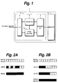
- Fig. 1 is a schematic diagram showing an example of a memory apparatus according to the present invention
- Fig. 2A and Fig. 2B are schematic diagrams for explaining an overwriting operation for data and an overwriting operation for reproducing operation count information according to the present invention
- Fig. 3 is a flow chart for explaining a first example of the data reading operation according to the embodiment of the present invention
- Fig. 4 is a flow chart for explaining a second example of the data reading operation according to the embodiment of the present invention
- Fig. 5 is a flow chart for explaining a third example of the data reading operation according to the embodiment of the present invention
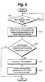
- Fig. 6 is a flow chart for explaining a fourth example of the data reading operation according to the embodiment of the present invention
- Fig. 1 is a schematic diagram showing an example of a memory apparatus according to the present invention
- Fig. 2A and Fig. 2B are schematic diagrams for explaining an overwriting operation for data and an overwriting operation for reproducing operation count information according to the present invention
- Fig. 3
- FIG. 7 is a flow chart for explaining a fifth example of the data reading operation according to the embodiment of the present invention.
- Fig. 8 is a flow chart for explaining a sixth example of the data reading operation according to the embodiment of the present invention; and
- Fig. 9 is a flow chart for explaining a seventh example of the data reading operation according to the embodiment of the present invention.
- FIG. 1 shows the structure of a memory apparatus according to the embodiment of the present invention.
- a host device (not shown) and a memory apparatus 1 are connected through for example a serial interface.
- the memory apparatus 1 has a control IC 2 and a memory 3.
- the memory apparatus 1 is formed in a card shape so that it can be attached and detached to and from the host device.
- the host device generates data to be written to the memory apparatus 1.
- the host device reads data from the memory apparatus 1 and performs a variety of data processes using data that has been read from the memory apparatus 1.
- the host device is for example a digital electronic camera.
- the host device writes a photographed picture to the memory apparatus 1.
- the host device reads a picture from the memory apparatus 1.
- Another example of the host device is an audio recording/reproducing apparatus. In this case, compressed audio data is written to the memory apparatus 1.
- compressed audio data is read from the memory apparatus 1.
- the control IC 2 has an interface 4, a register 5, a page buffer 6, an a memory interface 7.
- the interface 4 interfaces with the host device. Data (write data or read data and command data), a control signal, a power, and so forth are exchanged between the host device and the memory apparatus 1 through the interface 4.
- the register 5 stores addresses.
- the page buffer 6 temporarily stores write data or read data.
- the control IC 2 and the memory 3 may be integrated as one IC device. On the other hand, the control IC may not be composed of only one IC.
- the memory interface 7 is an interface disposed between the control IC 2 and the memory 3.
- the control IC 2 is provided with a sequencer (controller) composed of a CPU (not shown).
- the memory 3 is an irreversibly write memory that is a one-time-writable nonvolatile semiconductor memory.
- the memory 3 is referred to as OTP (One Time Programmable ROM).
- OTP One Time Programmable ROM
- data is read and written with a predetermined data amount at a time.
- the memory 3 is provided with a boot area that is read by the host device immediately after the memory is attached thereto. In the boot area, various types of information such as attribute information are prerecorded.
- Fig. 2 shows a state change of the memory.
- each square area represents a data unit for example a bit.
- Each white area represents a non-changed (initial state) data unit for example a "0" bit.
- Each black area represents a data unit that has been changed by the writing operation. In other words, each black area represents an irreversibly written data unit for example a "1" bit.
- the irreversibly written memory 3 may be provided with a counter area that records reproduction restriction information for example a data reading operation count value (reproducing operation count value) N.
- FIG. 3 is a flow chart showing an operation that simultaneously reads data from the memory apparatus 1 and erases data therefrom. This operation is controlled by a sequencer with which the control IC 2 is provided.
- step S1 shown in Fig. 3 it is determined whether or not a read request has been received from the host device.
- the flow advances to step S2.
- the read address is stored to the register 5.
- step S3 data is read from a designated address of the memory 3.
- the read data is stored to the page buffer 6.
- the data is output from the page buffer 6 to the host device through the interface 4.
- the read data may be directly supplied to the host side without an intervention of the page buffer 6.
- step S4 with reference to the read address stored in the register 5, the data of the address is erased.
- data can be read from the memory 3 only one time.
- Fig. 4 is a flow chart showing an example of another process.
- step S11 it is determined whether or not a read request has been received.
- the flow advances to step S12.
- step S12 it is determined whether or not there is a designated read address in a particular area.
- the particular area is a particular area of the memory 3 or the control IC 2.
- the particular area can be formed.
- the host device receives error information instead of read data corresponding to a read command that the host device has sent to the memory 3.
- the host device recognizes that it cannot read the data.
- the similar process is performed.
- step S14 the read address stored in the register 5 is written to the particular area.
- the read address is appended to the particular area.
- the particular area may have an address map. Address map data corresponding to the read address may be changed to the one that is prohibited from being read.
- step S12 the map may be referenced.
- step S25 of a flow chart shown in Fig. 5 a process that erases data that has been read from the memory 3 is added. Steps S21, S22, S23, and S24 shown in Fig. 5 correspond to steps S11, S12, S13, and S14 shown in Fig. 4, respectively.
- Fig. 6 is a flow chart showing an operation that designates the reproduction restriction value and that reads (reproduces) data from the memory 3 until the designated value becomes zero.
- the flow advance to step S32.
- the reproducing operation count value and the reproducing operation permission value are read from the particular area.
- the particular area is formed in the memory 3 or the control IC 2.
- the reproducing operation permission value is pre-written to the particular area.
- a copyright owner distributes a content such as video and/or audio data, he or she can record both the reproducing operation permission value and the content data to the memory apparatus. As a result, the copyright of the content data can be protected.
- the reproducing operation permission value is pre-designated for example eight. Whenever data is reproduced one time, one data unit is changed to the one that is prohibited from being written. The area shown in Fig. 2B is read at step S32. At step S33, it is determined whether or not the condition of (reproducing operation count value N ⁇ reproducing operation permission value?) is satisfied corresponding to the state of the particular area. When the condition is not satisfied, since (N ⁇ reproducing operation permission value), the reproducing operation is prohibited and thereby the process is terminated.
- step S34 data is read from the designated address of the memory 3.
- the read data is supplied to the host device through the page buffer 6 and the interface 4 (at step S34). Thereafter, the reproducing operation count value is appended to the particular area (at step S35).
- the operation shown in Fig. 6 controls the memory 3 so that after the host device has read data from the memory 3, the host device is prohibited from accessing the data without erasing the data from the memory 3. Alternatively, data stored in the memory 3 may be erased so that the host device is prevented from being accessing the data. As a result, the security of data may be more improved than the operation shown in Fig. 6.
- step S46 of a flow chart shown in Fig. 7 it is determined whether the condition of (reproducing operation count value N ⁇ reproducing operation permission value?) is satisfied. When the reproducing operation count value does not match the reproducing operation permission value, the process is terminated.
- step S46 When the determined result at step S46 represents that the reproducing operation count value N matches the reproducing operation permission value, the flow advances to step S47.
- step S47 meaningless data is overwritten to the memory 3.
- the read data is erased.
- Steps S41, S42, S43, S44, and S45 shown in Fig. 7 correspond to steps S31, S32, S33, S34, and S35 shown in Fig. 6, respectively.
- step S51 the determination result at step S51 shown in Fig. 8 represents that a read request has been received
- step S52 the reproducing operation permission value is read from the particular area.
- step S53 it is determined whether or not the condition of (reproducing operation permission value > 0?) is satisfied. When the determined result represents that the condition is not satisfied, the process is terminated.
- step S54 data is read from the memory 3 and supplied to the host device (at step S54).
- step S55 the reproducing operation count value is appended to the particular area.
- the reproducing operation permission value is decremented by 1.
- the reproducing operation permission value is pre-designated eight in the initial state. Whenever data is reproduced one time, the state of one data unit is changed. At step S52, the number of (white) data units that have not been changed is read as the reproducing operation permission value.
- the operation shown in Fig. 8 controls the memory 3 so that the host device is prohibited from accessing data that has been read from the memory 3 without erasing the data from the memory 3.
- data may be erased from the memory 3 so that the host device cannot access the data at all.
- the security of data can be more improved than the operation shown in Fig. 8.
- step S66 of a flow chart shown in Fig. 9 it is determined whether or not the condition of (reproducing operation permission value > 0?) is satisfied. When the condition is satisfied (namely, the reproducing operation can be further performed), the process is terminated. In contrast, when the determined result at step S66 represents that the condition is not satisfied, the flow advances to step S67. At step S67, the read data is erased.
- Steps S61, S62, S63, S64, and S65 shown in Fig. 9 correspond to steps S51, S52, S53, S54, and S55 shown in Fig. 8, respectively.
- the forgoing embodiment of the present invention can be applied to key data that decrypts encrypted data so as to erase or restrict the number of times of reproducing operation for the key data in the forgoing manner.
- the present invention is not limited to the forgoing embodiment.
- various modifications and applications of the present invention are available without departing from the spirit of the present invention.
- the number of times of reproducing operation is restricted.
- the total time or valid period (from start date to end date) for which data can be reproduced may be recorded in the irreversibly write memory.
- the present invention can be applied to cash, electronic money, and prepaid card that records points or the like that permit a reproducing operation.
- data is updated.
- the present invention can be applied to a delivery for an initial password. In this case, when the initial password is read, it is erased. As a result, the security of the initial password is protected.
- the present invention when data is read, the data that has been read is overwritten so that the data is prohibited from being irreversibly written. Thus, even if the memory device is disassembled and the memory is removed, it is impossible to read internal data. As a result, high security is assured.
- a flash memory When a flash memory is used, a special structure that prevents the memory from being illegally accessed should be provided. As a result, the cost of the apparatus adversely rises. In contrast, the cost of the irreversibly write memory is lower than the cost of the flash memory.
- the present invention when the present invention is applied to the irreversibly write memory, a special structure that assures the security of data is not required. Thus, the cost of the apparatus can be further reduced.
- reproduction restriction information is written to the irreversibly write memory. As a result, the reproduction restriction information can be prevented from being forged.
Landscapes
- Engineering & Computer Science (AREA)
- Theoretical Computer Science (AREA)
- General Physics & Mathematics (AREA)
- Physics & Mathematics (AREA)
- Business, Economics & Management (AREA)
- Computer Security & Cryptography (AREA)
- General Engineering & Computer Science (AREA)
- Microelectronics & Electronic Packaging (AREA)
- Computer Networks & Wireless Communication (AREA)
- Computer Hardware Design (AREA)
- Accounting & Taxation (AREA)
- Strategic Management (AREA)
- General Business, Economics & Management (AREA)
- Software Systems (AREA)
- Storage Device Security (AREA)
- Read Only Memory (AREA)
Abstract
Description
Claims (5)
- A memory apparatus, comprising:wherein when data that has been written is read, after data is read from the memory to the data buffer circuit, a data area on the memory from which the data has been read is overwritten so that the data area is prohibited from being read.an irreversibly write memory;a control circuit that controls a writing operation and a reading operation for the irreversibly write memory; anda data buffer circuit,
- A memory apparatus, comprising:wherein an area that stores reproduction restriction information is formed in the irreversibly write memory or in an irreversibly write memory disposed in the control circuit, andan irreversibly write memory;a control circuit that controls a writing operation and a reading operation for the irreversibly write memory; anda data buffer circuit,
wherein when data that has been written is read, if the reading operation is restricted by the reproduction restriction information, the reading operation is prohibited. - A memory apparatus, comprising:wherein an area that stores a reading operation count value that represents that the number of times of which data has been read from the memory is formed in the irreversibly write memory or in an irreversibly write memory of the control circuit,an irreversibly write memory;a control circuit that controls a writing operation and a reading operation for the irreversibly write memory; anda data buffer circuit,
wherein when data that has been written is read, the area that stores the reading operation count value is overwritten so that the area is prohibited from being read, and
wherein when all the area that stores the reading operation count value has been prohibited from being read, the reading operation is prohibited. - The memory apparatus as set forth in claim 3,
wherein when all the area that stores the reading operation count value has been prohibited from being read, the data area on the memory from which the data has been read is overwritten so that the data area is prohibited from being read. - The memory apparatus as set forth in claim 1, 2, or 3,
wherein the irreversibly write memory is a nonvolatile semiconductor memory that can be attached and detached to and from the host device.
Applications Claiming Priority (3)
| Application Number | Priority Date | Filing Date | Title |
|---|---|---|---|
| JP2000307200 | 2000-10-06 | ||
| JP2000307200A JP4770012B2 (en) | 2000-10-06 | 2000-10-06 | Memory device |
| PCT/JP2001/008794 WO2002031663A1 (en) | 2000-10-06 | 2001-10-05 | Memory device |
Publications (2)
| Publication Number | Publication Date |
|---|---|
| EP1324205A1 true EP1324205A1 (en) | 2003-07-02 |
| EP1324205A4 EP1324205A4 (en) | 2004-12-29 |
Family
ID=18787750
Family Applications (1)
| Application Number | Title | Priority Date | Filing Date |
|---|---|---|---|
| EP01974708A Withdrawn EP1324205A4 (en) | 2000-10-06 | 2001-10-05 | MEMORY |
Country Status (6)
| Country | Link |
|---|---|
| US (1) | US7167943B2 (en) |
| EP (1) | EP1324205A4 (en) |
| JP (1) | JP4770012B2 (en) |
| KR (1) | KR20030036890A (en) |
| CN (1) | CN1290023C (en) |
| WO (1) | WO2002031663A1 (en) |
Families Citing this family (16)
| Publication number | Priority date | Publication date | Assignee | Title |
|---|---|---|---|---|
| US7890771B2 (en) * | 2002-04-17 | 2011-02-15 | Microsoft Corporation | Saving and retrieving data based on public key encryption |
| EP1795992B1 (en) | 2002-07-30 | 2018-01-24 | Fujitsu Limited | Method and apparatus for reproducing information using a security module |
| JP2008505347A (en) * | 2004-07-02 | 2008-02-21 | 新世代株式会社 | Data distribution system, data acquisition device, writing device, data acquisition program, data acquisition method, recording medium, data distribution device, and content distribution system |
| JP4720140B2 (en) * | 2004-10-01 | 2011-07-13 | 船井電機株式会社 | Information processing device |
| JP4713878B2 (en) * | 2004-12-14 | 2011-06-29 | 株式会社東芝 | Portable electronic device |
| TWI325532B (en) * | 2006-09-14 | 2010-06-01 | Novatek Microelectronics Corp | Controlling circuit and method for power saving |
| US20090235040A1 (en) * | 2008-03-14 | 2009-09-17 | Chilumula Ajaya K | Programmble memory appratus, systems, and methods |
| JP5365239B2 (en) * | 2009-02-17 | 2013-12-11 | 凸版印刷株式会社 | IC card issuance system |
| JP5347649B2 (en) * | 2009-03-30 | 2013-11-20 | 凸版印刷株式会社 | Nonvolatile semiconductor memory device |
| JP4945655B2 (en) * | 2010-04-13 | 2012-06-06 | 株式会社リコー | Information processing apparatus, image processing apparatus, information processing method, computer program, and recording medium |
| DE102010052224A1 (en) | 2010-11-24 | 2012-05-24 | Giesecke & Devrient Secure Flash Solutions Gmbh | Storage medium and method for operating a storage medium |
| JP5734492B1 (en) * | 2014-05-08 | 2015-06-17 | ウィンボンド エレクトロニクス コーポレーション | Semiconductor memory device |
| US10888119B2 (en) * | 2014-07-10 | 2021-01-12 | Rai Strategic Holdings, Inc. | System and related methods, apparatuses, and computer program products for controlling operation of a device based on a read request |
| JP2022010951A (en) * | 2020-06-29 | 2022-01-17 | キオクシア株式会社 | Semiconductor storage device |
| JP7330157B2 (en) * | 2020-09-18 | 2023-08-21 | 株式会社東芝 | Information processing device and update processing method |
| US20240160794A1 (en) * | 2022-11-10 | 2024-05-16 | Samsung Electronics Co., Ltd. | Operating method of storage device and operating method of storage system including storage device |
Family Cites Families (26)
| Publication number | Priority date | Publication date | Assignee | Title |
|---|---|---|---|---|
| US3576549A (en) * | 1969-04-14 | 1971-04-27 | Cogar Corp | Semiconductor device, method, and memory array |
| US4691299A (en) * | 1982-04-30 | 1987-09-01 | Massachusetts Institute Of Technology | Method and apparatus for reusing non-erasable memory media |
| JPH0756667B2 (en) | 1986-02-17 | 1995-06-14 | 日本電信電話株式会社 | How to use the card |
| JPS63123184A (en) * | 1986-11-12 | 1988-05-26 | Omron Tateisi Electronics Co | Ic card |
| JPS63153633A (en) * | 1986-12-17 | 1988-06-27 | Nec Corp | Use limitation system for program |
| US5202852A (en) * | 1989-02-09 | 1993-04-13 | Mitsubishi Denki Kabushiki Kaisha | Programmable read only memory card with improved buffer circuit |
| US5032708A (en) * | 1989-08-10 | 1991-07-16 | International Business Machines Corp. | Write-once-read-once batteryless authentication token |
| US5233576A (en) * | 1989-10-25 | 1993-08-03 | Hewlett-Packard Company | Multi-function optical disk drive and media |
| JPH064996A (en) * | 1992-06-19 | 1994-01-14 | Tatsuo Yano | Control system of frequency and duration of reproduction of digitized music and video or the like |
| FR2709582B1 (en) * | 1993-09-02 | 1995-09-29 | Gemplus Card Int | Electronic payment method, in particular by means of a smart card. |
| JPH07244781A (en) * | 1994-03-07 | 1995-09-19 | C S K Sogo Kenkyusho:Kk | Software rental method and device and distribution medium |
| US5644444A (en) * | 1995-03-10 | 1997-07-01 | Iomega Corporation | Read/write protect scheme for a disk cartridge and drive |
| JP3461234B2 (en) * | 1996-01-22 | 2003-10-27 | 株式会社東芝 | Data protection circuit |
| JPH10134160A (en) * | 1996-10-28 | 1998-05-22 | Miyuucom:Kk | Forging preventing mechanism for prepaid card |
| JPH10208002A (en) * | 1997-01-20 | 1998-08-07 | Pioneer Electron Corp | Information read control method and information reader |
| JPH10269144A (en) * | 1997-03-24 | 1998-10-09 | Sony Corp | Information recording / reproducing method and device, information providing method and device, and information recording medium |
| JPH11110294A (en) * | 1997-10-01 | 1999-04-23 | Toshiba Corp | Microcomputer and information processing device |
| US6226698B1 (en) * | 1997-11-10 | 2001-05-01 | Sun Microsystems, Inc. | Method and apparatus for dynamically calculating degrees of fullness of a synchronous FIFO |
| JP3482989B2 (en) | 1998-08-04 | 2004-01-06 | ソニー株式会社 | Optical disc reproducing method, optical disc recording / reproducing method, optical disc reproducing apparatus, optical disc recording / reproducing apparatus, and optical disc |
| JP3454165B2 (en) * | 1998-09-14 | 2003-10-06 | 株式会社豊田中央研究所 | Information recording medium and information recording method |
| US6304948B1 (en) | 1998-10-06 | 2001-10-16 | Ricoh Corporation | Method and apparatus for erasing data after expiration |
| JP3537684B2 (en) * | 1998-11-02 | 2004-06-14 | 松下電器産業株式会社 | Recording / reproducing device, program recording medium |
| FR2790854A1 (en) * | 1998-12-01 | 2000-09-15 | Philippe Baron D | Device for securing computer data exchanges of payment or remote payment has inaccessible area in secret memory in which primary codes of list may be used as preference for secure exchange |
| GB9914711D0 (en) * | 1999-06-23 | 1999-08-25 | Leck Michael J | Electronic seal,methods and security system |
| US20010025343A1 (en) * | 2000-03-27 | 2001-09-27 | Roy Chrisop | Random bit mask generation for obscuring data on nonvolatile memory device |
| US6658438B1 (en) * | 2000-08-14 | 2003-12-02 | Matrix Semiconductor, Inc. | Method for deleting stored digital data from write-once memory device |
-
2000
- 2000-10-06 JP JP2000307200A patent/JP4770012B2/en not_active Expired - Fee Related
-
2001
- 2001-10-05 KR KR10-2003-7004821A patent/KR20030036890A/en not_active Ceased
- 2001-10-05 US US10/149,142 patent/US7167943B2/en not_active Expired - Fee Related
- 2001-10-05 CN CNB018199143A patent/CN1290023C/en not_active Expired - Fee Related
- 2001-10-05 WO PCT/JP2001/008794 patent/WO2002031663A1/en not_active Ceased
- 2001-10-05 EP EP01974708A patent/EP1324205A4/en not_active Withdrawn
Also Published As
| Publication number | Publication date |
|---|---|
| JP4770012B2 (en) | 2011-09-07 |
| CN1290023C (en) | 2006-12-13 |
| WO2002031663A1 (en) | 2002-04-18 |
| KR20030036890A (en) | 2003-05-09 |
| US7167943B2 (en) | 2007-01-23 |
| US20030084258A1 (en) | 2003-05-01 |
| EP1324205A4 (en) | 2004-12-29 |
| CN1478231A (en) | 2004-02-25 |
| JP2002116959A (en) | 2002-04-19 |
Similar Documents
| Publication | Publication Date | Title |
|---|---|---|
| EP1324205A1 (en) | Memory device | |
| US6912619B2 (en) | Memory apparatus, data-processing apparatus, and data-processing method | |
| US9098440B2 (en) | Secure compact flash | |
| US8296582B2 (en) | Method and system for providing copy-protection on a storage medium and storage medium for use in such a system | |
| US20040215909A1 (en) | Nonvolatile memory device and data processing system | |
| JPWO2000013089A1 (en) | Storage device, processing device, and processing method | |
| JP4101975B2 (en) | Data recording / reproducing apparatus using portable storage medium | |
| US6732246B2 (en) | Memory apparatus and memory access restricting method | |
| US8429401B2 (en) | Method and apparatus for virtually erasing data from WORM storage devices | |
| JP2000298942A (en) | Disk storage device and copy protection system applied to the device | |
| JP3893805B2 (en) | Data reader | |
| JP4936834B2 (en) | Data protection method for semiconductor memory card and semiconductor memory card | |
| JPH07161172A (en) | Data recording medium | |
| US20030056106A1 (en) | Encryption system for preventing data from being copied illegally and method of the same | |
| JP2001283170A (en) | Semiconductor memory and authenticating system using the same memory | |
| JPH06187511A (en) | Information recording / reproducing system | |
| US20060007738A1 (en) | Area management type memory system, area management type memory unit and area management type memory controller | |
| JPS63301387A (en) | Ic card system | |
| JP2003346106A (en) | Record editing device | |
| JP2005149138A (en) | Method for reading data from storage medium and its apparatus | |
| JPH0778230A (en) | Memory card device | |
| JPS63223994A (en) | Portable electronic equipment | |
| KR19990042063A (en) | Magnetic recording / playback apparatus and method for setting and releasing recording protection of magnetic recording media including memory | |
| JP2004118885A (en) | Method of erasing information of write once memory |
Legal Events
| Date | Code | Title | Description |
|---|---|---|---|
| PUAI | Public reference made under article 153(3) epc to a published international application that has entered the european phase |
Free format text: ORIGINAL CODE: 0009012 |
|
| 17P | Request for examination filed |
Effective date: 20030401 |
|
| AK | Designated contracting states |
Designated state(s): AT BE CH CY DE DK ES FI FR GB GR IE IT LI LU MC NL PT SE TR |
|
| RBV | Designated contracting states (corrected) |
Designated state(s): DE FR GB |
|
| A4 | Supplementary search report drawn up and despatched |
Effective date: 20041116 |
|
| RIC1 | Information provided on ipc code assigned before grant |
Ipc: 7G 06F 1/00 B Ipc: 7G 06F 12/14 A Ipc: 7G 06K 17/00 B Ipc: 7G 06K 19/00 B |
|
| STAA | Information on the status of an ep patent application or granted ep patent |
Free format text: STATUS: THE APPLICATION IS DEEMED TO BE WITHDRAWN |
|
| 18D | Application deemed to be withdrawn |
Effective date: 20080610 |