EP1323671A1 - Procédé de fabrication d'au moins un nanotube entre deux éléments électriquement conducteurs et dispositif pour mettre en oeuvre un tel procédé - Google Patents
Procédé de fabrication d'au moins un nanotube entre deux éléments électriquement conducteurs et dispositif pour mettre en oeuvre un tel procédé Download PDFInfo
- Publication number
- EP1323671A1 EP1323671A1 EP02293242A EP02293242A EP1323671A1 EP 1323671 A1 EP1323671 A1 EP 1323671A1 EP 02293242 A EP02293242 A EP 02293242A EP 02293242 A EP02293242 A EP 02293242A EP 1323671 A1 EP1323671 A1 EP 1323671A1
- Authority
- EP
- European Patent Office
- Prior art keywords
- deposition chamber
- zone
- magnetic field
- substrate
- electrically conductive
- Prior art date
- Legal status (The legal status is an assumption and is not a legal conclusion. Google has not performed a legal analysis and makes no representation as to the accuracy of the status listed.)
- Granted
Links
- 239000002071 nanotube Substances 0.000 title claims abstract description 52
- 238000000034 method Methods 0.000 title claims abstract description 46
- 238000004519 manufacturing process Methods 0.000 title claims abstract description 17
- 230000008569 process Effects 0.000 title claims description 12
- 230000008021 deposition Effects 0.000 claims abstract description 44
- 239000000758 substrate Substances 0.000 claims abstract description 36
- 238000010494 dissociation reaction Methods 0.000 claims abstract description 11
- 230000005593 dissociations Effects 0.000 claims abstract description 11
- 238000012216 screening Methods 0.000 claims abstract description 10
- 238000002347 injection Methods 0.000 claims description 24
- 239000007924 injection Substances 0.000 claims description 24
- OKTJSMMVPCPJKN-UHFFFAOYSA-N Carbon Chemical compound [C] OKTJSMMVPCPJKN-UHFFFAOYSA-N 0.000 claims description 20
- 229910052799 carbon Inorganic materials 0.000 claims description 18
- 150000002500 ions Chemical class 0.000 claims description 12
- 239000002184 metal Substances 0.000 claims description 12
- 229910052751 metal Inorganic materials 0.000 claims description 12
- XEEYBQQBJWHFJM-UHFFFAOYSA-N Iron Chemical compound [Fe] XEEYBQQBJWHFJM-UHFFFAOYSA-N 0.000 claims description 6
- PXHVJJICTQNCMI-UHFFFAOYSA-N Nickel Chemical compound [Ni] PXHVJJICTQNCMI-UHFFFAOYSA-N 0.000 claims description 6
- 238000010438 heat treatment Methods 0.000 claims description 6
- 150000001335 aliphatic alkanes Chemical class 0.000 claims description 3
- 150000001336 alkenes Chemical class 0.000 claims description 3
- 150000001345 alkine derivatives Chemical class 0.000 claims description 3
- 239000000956 alloy Substances 0.000 claims description 3
- 229910045601 alloy Inorganic materials 0.000 claims description 3
- 238000013459 approach Methods 0.000 claims description 3
- 229910017052 cobalt Inorganic materials 0.000 claims description 3
- 239000010941 cobalt Substances 0.000 claims description 3
- GUTLYIVDDKVIGB-UHFFFAOYSA-N cobalt atom Chemical compound [Co] GUTLYIVDDKVIGB-UHFFFAOYSA-N 0.000 claims description 3
- 229910052742 iron Inorganic materials 0.000 claims description 3
- 239000000203 mixture Substances 0.000 claims description 3
- 229910052759 nickel Inorganic materials 0.000 claims description 3
- 230000005684 electric field Effects 0.000 claims description 2
- 230000001737 promoting effect Effects 0.000 claims description 2
- 238000000151 deposition Methods 0.000 description 23
- 241000894007 species Species 0.000 description 14
- 238000005229 chemical vapour deposition Methods 0.000 description 6
- VNWKTOKETHGBQD-UHFFFAOYSA-N methane Chemical compound C VNWKTOKETHGBQD-UHFFFAOYSA-N 0.000 description 6
- 230000003197 catalytic effect Effects 0.000 description 4
- 239000004020 conductor Substances 0.000 description 4
- 239000002070 nanowire Substances 0.000 description 4
- 230000010349 pulsation Effects 0.000 description 4
- HSFWRNGVRCDJHI-UHFFFAOYSA-N alpha-acetylene Natural products C#C HSFWRNGVRCDJHI-UHFFFAOYSA-N 0.000 description 3
- 125000004432 carbon atom Chemical group C* 0.000 description 3
- 238000006356 dehydrogenation reaction Methods 0.000 description 3
- 125000002534 ethynyl group Chemical group [H]C#C* 0.000 description 3
- 230000004913 activation Effects 0.000 description 2
- 230000008901 benefit Effects 0.000 description 2
- 239000002041 carbon nanotube Substances 0.000 description 2
- 229910021393 carbon nanotube Inorganic materials 0.000 description 2
- 238000006243 chemical reaction Methods 0.000 description 2
- 230000015654 memory Effects 0.000 description 2
- 238000005240 physical vapour deposition Methods 0.000 description 2
- 238000001556 precipitation Methods 0.000 description 2
- 239000000126 substance Substances 0.000 description 2
- 239000012808 vapor phase Substances 0.000 description 2
- 241000239290 Araneae Species 0.000 description 1
- 229910004298 SiO 2 Inorganic materials 0.000 description 1
- PNEYBMLMFCGWSK-UHFFFAOYSA-N aluminium oxide Inorganic materials [O-2].[O-2].[O-2].[Al+3].[Al+3] PNEYBMLMFCGWSK-UHFFFAOYSA-N 0.000 description 1
- 230000015572 biosynthetic process Effects 0.000 description 1
- 239000003054 catalyst Substances 0.000 description 1
- 238000004140 cleaning Methods 0.000 description 1
- 230000002301 combined effect Effects 0.000 description 1
- 150000001875 compounds Chemical class 0.000 description 1
- 238000001816 cooling Methods 0.000 description 1
- 230000002349 favourable effect Effects 0.000 description 1
- 230000005669 field effect Effects 0.000 description 1
- 230000003902 lesion Effects 0.000 description 1
- 239000000463 material Substances 0.000 description 1
- 238000012986 modification Methods 0.000 description 1
- 230000004048 modification Effects 0.000 description 1
- 238000005442 molecular electronic Methods 0.000 description 1
- 238000005289 physical deposition Methods 0.000 description 1
- 230000001681 protective effect Effects 0.000 description 1
- 239000010453 quartz Substances 0.000 description 1
- 229910052710 silicon Inorganic materials 0.000 description 1
- 239000010703 silicon Substances 0.000 description 1
- VYPSYNLAJGMNEJ-UHFFFAOYSA-N silicon dioxide Inorganic materials O=[Si]=O VYPSYNLAJGMNEJ-UHFFFAOYSA-N 0.000 description 1
- 239000002109 single walled nanotube Substances 0.000 description 1
- 239000007787 solid Substances 0.000 description 1
- 239000000243 solution Substances 0.000 description 1
- 238000003892 spreading Methods 0.000 description 1
- 230000007480 spreading Effects 0.000 description 1
- 239000010935 stainless steel Substances 0.000 description 1
- 229910001220 stainless steel Inorganic materials 0.000 description 1
- 238000012800 visualization Methods 0.000 description 1
Images

Classifications
-
- C—CHEMISTRY; METALLURGY
- C01—INORGANIC CHEMISTRY
- C01B—NON-METALLIC ELEMENTS; COMPOUNDS THEREOF; METALLOIDS OR COMPOUNDS THEREOF NOT COVERED BY SUBCLASS C01C
- C01B32/00—Carbon; Compounds thereof
- C01B32/15—Nano-sized carbon materials
- C01B32/158—Carbon nanotubes
- C01B32/16—Preparation
-
- B—PERFORMING OPERATIONS; TRANSPORTING
- B82—NANOTECHNOLOGY
- B82Y—SPECIFIC USES OR APPLICATIONS OF NANOSTRUCTURES; MEASUREMENT OR ANALYSIS OF NANOSTRUCTURES; MANUFACTURE OR TREATMENT OF NANOSTRUCTURES
- B82Y10/00—Nanotechnology for information processing, storage or transmission, e.g. quantum computing or single electron logic
-
- B—PERFORMING OPERATIONS; TRANSPORTING
- B82—NANOTECHNOLOGY
- B82Y—SPECIFIC USES OR APPLICATIONS OF NANOSTRUCTURES; MEASUREMENT OR ANALYSIS OF NANOSTRUCTURES; MANUFACTURE OR TREATMENT OF NANOSTRUCTURES
- B82Y30/00—Nanotechnology for materials or surface science, e.g. nanocomposites
-
- B—PERFORMING OPERATIONS; TRANSPORTING
- B82—NANOTECHNOLOGY
- B82Y—SPECIFIC USES OR APPLICATIONS OF NANOSTRUCTURES; MEASUREMENT OR ANALYSIS OF NANOSTRUCTURES; MANUFACTURE OR TREATMENT OF NANOSTRUCTURES
- B82Y40/00—Manufacture or treatment of nanostructures
-
- C—CHEMISTRY; METALLURGY
- C23—COATING METALLIC MATERIAL; COATING MATERIAL WITH METALLIC MATERIAL; CHEMICAL SURFACE TREATMENT; DIFFUSION TREATMENT OF METALLIC MATERIAL; COATING BY VACUUM EVAPORATION, BY SPUTTERING, BY ION IMPLANTATION OR BY CHEMICAL VAPOUR DEPOSITION, IN GENERAL; INHIBITING CORROSION OF METALLIC MATERIAL OR INCRUSTATION IN GENERAL
- C23C—COATING METALLIC MATERIAL; COATING MATERIAL WITH METALLIC MATERIAL; SURFACE TREATMENT OF METALLIC MATERIAL BY DIFFUSION INTO THE SURFACE, BY CHEMICAL CONVERSION OR SUBSTITUTION; COATING BY VACUUM EVAPORATION, BY SPUTTERING, BY ION IMPLANTATION OR BY CHEMICAL VAPOUR DEPOSITION, IN GENERAL
- C23C16/00—Chemical coating by decomposition of gaseous compounds, without leaving reaction products of surface material in the coating, i.e. chemical vapour deposition [CVD] processes
- C23C16/22—Chemical coating by decomposition of gaseous compounds, without leaving reaction products of surface material in the coating, i.e. chemical vapour deposition [CVD] processes characterised by the deposition of inorganic material, other than metallic material
- C23C16/26—Deposition of carbon only
-
- C—CHEMISTRY; METALLURGY
- C23—COATING METALLIC MATERIAL; COATING MATERIAL WITH METALLIC MATERIAL; CHEMICAL SURFACE TREATMENT; DIFFUSION TREATMENT OF METALLIC MATERIAL; COATING BY VACUUM EVAPORATION, BY SPUTTERING, BY ION IMPLANTATION OR BY CHEMICAL VAPOUR DEPOSITION, IN GENERAL; INHIBITING CORROSION OF METALLIC MATERIAL OR INCRUSTATION IN GENERAL
- C23C—COATING METALLIC MATERIAL; COATING MATERIAL WITH METALLIC MATERIAL; SURFACE TREATMENT OF METALLIC MATERIAL BY DIFFUSION INTO THE SURFACE, BY CHEMICAL CONVERSION OR SUBSTITUTION; COATING BY VACUUM EVAPORATION, BY SPUTTERING, BY ION IMPLANTATION OR BY CHEMICAL VAPOUR DEPOSITION, IN GENERAL
- C23C16/00—Chemical coating by decomposition of gaseous compounds, without leaving reaction products of surface material in the coating, i.e. chemical vapour deposition [CVD] processes
- C23C16/44—Chemical coating by decomposition of gaseous compounds, without leaving reaction products of surface material in the coating, i.e. chemical vapour deposition [CVD] processes characterised by the method of coating
- C23C16/50—Chemical coating by decomposition of gaseous compounds, without leaving reaction products of surface material in the coating, i.e. chemical vapour deposition [CVD] processes characterised by the method of coating using electric discharges
- C23C16/511—Chemical coating by decomposition of gaseous compounds, without leaving reaction products of surface material in the coating, i.e. chemical vapour deposition [CVD] processes characterised by the method of coating using electric discharges using microwave discharges
-
- C—CHEMISTRY; METALLURGY
- C30—CRYSTAL GROWTH
- C30B—SINGLE-CRYSTAL GROWTH; UNIDIRECTIONAL SOLIDIFICATION OF EUTECTIC MATERIAL OR UNIDIRECTIONAL DEMIXING OF EUTECTOID MATERIAL; REFINING BY ZONE-MELTING OF MATERIAL; PRODUCTION OF A HOMOGENEOUS POLYCRYSTALLINE MATERIAL WITH DEFINED STRUCTURE; SINGLE CRYSTALS OR HOMOGENEOUS POLYCRYSTALLINE MATERIAL WITH DEFINED STRUCTURE; AFTER-TREATMENT OF SINGLE CRYSTALS OR A HOMOGENEOUS POLYCRYSTALLINE MATERIAL WITH DEFINED STRUCTURE; APPARATUS THEREFOR
- C30B25/00—Single-crystal growth by chemical reaction of reactive gases, e.g. chemical vapour-deposition growth
- C30B25/02—Epitaxial-layer growth
- C30B25/10—Heating of the reaction chamber or the substrate
- C30B25/105—Heating of the reaction chamber or the substrate by irradiation or electric discharge
-
- C—CHEMISTRY; METALLURGY
- C30—CRYSTAL GROWTH
- C30B—SINGLE-CRYSTAL GROWTH; UNIDIRECTIONAL SOLIDIFICATION OF EUTECTIC MATERIAL OR UNIDIRECTIONAL DEMIXING OF EUTECTOID MATERIAL; REFINING BY ZONE-MELTING OF MATERIAL; PRODUCTION OF A HOMOGENEOUS POLYCRYSTALLINE MATERIAL WITH DEFINED STRUCTURE; SINGLE CRYSTALS OR HOMOGENEOUS POLYCRYSTALLINE MATERIAL WITH DEFINED STRUCTURE; AFTER-TREATMENT OF SINGLE CRYSTALS OR A HOMOGENEOUS POLYCRYSTALLINE MATERIAL WITH DEFINED STRUCTURE; APPARATUS THEREFOR
- C30B29/00—Single crystals or homogeneous polycrystalline material with defined structure characterised by the material or by their shape
- C30B29/02—Elements
-
- C—CHEMISTRY; METALLURGY
- C30—CRYSTAL GROWTH
- C30B—SINGLE-CRYSTAL GROWTH; UNIDIRECTIONAL SOLIDIFICATION OF EUTECTIC MATERIAL OR UNIDIRECTIONAL DEMIXING OF EUTECTOID MATERIAL; REFINING BY ZONE-MELTING OF MATERIAL; PRODUCTION OF A HOMOGENEOUS POLYCRYSTALLINE MATERIAL WITH DEFINED STRUCTURE; SINGLE CRYSTALS OR HOMOGENEOUS POLYCRYSTALLINE MATERIAL WITH DEFINED STRUCTURE; AFTER-TREATMENT OF SINGLE CRYSTALS OR A HOMOGENEOUS POLYCRYSTALLINE MATERIAL WITH DEFINED STRUCTURE; APPARATUS THEREFOR
- C30B29/00—Single crystals or homogeneous polycrystalline material with defined structure characterised by the material or by their shape
- C30B29/60—Single crystals or homogeneous polycrystalline material with defined structure characterised by the material or by their shape characterised by shape
- C30B29/605—Products containing multiple oriented crystallites, e.g. columnar crystallites
-
- H—ELECTRICITY
- H01—ELECTRIC ELEMENTS
- H01J—ELECTRIC DISCHARGE TUBES OR DISCHARGE LAMPS
- H01J37/00—Discharge tubes with provision for introducing objects or material to be exposed to the discharge, e.g. for the purpose of examination or processing thereof
- H01J37/32—Gas-filled discharge tubes
- H01J37/32009—Arrangements for generation of plasma specially adapted for examination or treatment of objects, e.g. plasma sources
- H01J37/32192—Microwave generated discharge
-
- H—ELECTRICITY
- H01—ELECTRIC ELEMENTS
- H01J—ELECTRIC DISCHARGE TUBES OR DISCHARGE LAMPS
- H01J37/00—Discharge tubes with provision for introducing objects or material to be exposed to the discharge, e.g. for the purpose of examination or processing thereof
- H01J37/32—Gas-filled discharge tubes
- H01J37/32431—Constructional details of the reactor
- H01J37/3266—Magnetic control means
-
- H—ELECTRICITY
- H05—ELECTRIC TECHNIQUES NOT OTHERWISE PROVIDED FOR
- H05H—PLASMA TECHNIQUE; PRODUCTION OF ACCELERATED ELECTRICALLY-CHARGED PARTICLES OR OF NEUTRONS; PRODUCTION OR ACCELERATION OF NEUTRAL MOLECULAR OR ATOMIC BEAMS
- H05H1/00—Generating plasma; Handling plasma
- H05H1/24—Generating plasma
- H05H1/46—Generating plasma using applied electromagnetic fields, e.g. high frequency or microwave energy
-
- H—ELECTRICITY
- H10—SEMICONDUCTOR DEVICES; ELECTRIC SOLID-STATE DEVICES NOT OTHERWISE PROVIDED FOR
- H10K—ORGANIC ELECTRIC SOLID-STATE DEVICES
- H10K85/00—Organic materials used in the body or electrodes of devices covered by this subclass
- H10K85/20—Carbon compounds, e.g. carbon nanotubes or fullerenes
- H10K85/221—Carbon nanotubes
-
- H—ELECTRICITY
- H10—SEMICONDUCTOR DEVICES; ELECTRIC SOLID-STATE DEVICES NOT OTHERWISE PROVIDED FOR
- H10K—ORGANIC ELECTRIC SOLID-STATE DEVICES
- H10K85/00—Organic materials used in the body or electrodes of devices covered by this subclass
- H10K85/60—Organic compounds having low molecular weight
- H10K85/615—Polycyclic condensed aromatic hydrocarbons, e.g. anthracene
-
- Y—GENERAL TAGGING OF NEW TECHNOLOGICAL DEVELOPMENTS; GENERAL TAGGING OF CROSS-SECTIONAL TECHNOLOGIES SPANNING OVER SEVERAL SECTIONS OF THE IPC; TECHNICAL SUBJECTS COVERED BY FORMER USPC CROSS-REFERENCE ART COLLECTIONS [XRACs] AND DIGESTS
- Y10—TECHNICAL SUBJECTS COVERED BY FORMER USPC
- Y10S—TECHNICAL SUBJECTS COVERED BY FORMER USPC CROSS-REFERENCE ART COLLECTIONS [XRACs] AND DIGESTS
- Y10S427/00—Coating processes
- Y10S427/102—Fullerene type base or coating
-
- Y—GENERAL TAGGING OF NEW TECHNOLOGICAL DEVELOPMENTS; GENERAL TAGGING OF CROSS-SECTIONAL TECHNOLOGIES SPANNING OVER SEVERAL SECTIONS OF THE IPC; TECHNICAL SUBJECTS COVERED BY FORMER USPC CROSS-REFERENCE ART COLLECTIONS [XRACs] AND DIGESTS
- Y10—TECHNICAL SUBJECTS COVERED BY FORMER USPC
- Y10S—TECHNICAL SUBJECTS COVERED BY FORMER USPC CROSS-REFERENCE ART COLLECTIONS [XRACs] AND DIGESTS
- Y10S977/00—Nanotechnology
- Y10S977/84—Manufacture, treatment, or detection of nanostructure
- Y10S977/842—Manufacture, treatment, or detection of nanostructure for carbon nanotubes or fullerenes
- Y10S977/843—Gas phase catalytic growth, i.e. chemical vapor deposition
Definitions
- nanotubes we mean tubes having carbon atoms, the diameter of which is between a few nanometers and a few tens of nanometers, and preferably from 1 to 100 nm.
- Such sets consisting of two electrically conductive elements interconnected by a nanotube, are used in particular of the realization of nano-components for the field of molecular electronics.
- these sets can find an application in the field effect transistors, memories of the RAM type or any type of electronic junction.
- the sets mentioned above may also apply to the field of biotechnology, as part of the realization of nano-sensors chemical or biosensors by grafting molecules.
- CVD method translated from English “Chemical Vapor Deposition” deposition methods translated from English “Chemical Vapor Deposition”
- hybrid CVD methods consisting in implementing a CVD method combined with plasma created by microwaves or by filament.
- a first approach described in document “H. Postma et al., Advanced Material No. 17 P.1299 (2000) “, consists in manufacturing a plurality of nanotubes before spreading them on a substrate. It is then necessary to manipulate them so as to position correctly with respect to the electrodes to connect and then make the metal connection with these electrodes.
- connection to the electrodes of the nanotubes is made during the manufacture of these, the method proposed remains uncontrollable as to the number of nanotubes made between these two electrodes. Moreover, we also do not fully control the quality of junction, which forces to keep only the nanotubes for which connection to electrodes was carried out smoothly and successfully.
- the purpose of the present invention is therefore to to present a process for manufacturing nanotubes two electrically conductive elements, remedying the least partially to the disadvantages mentioned above, relating to the achievements of the prior art.
- Another object of the invention is to present a device likely to implement a manufacturing process, such as that corresponding to purpose mentioned above.
- the invention first of all relates to a process for manufacturing at least one nanotube between two electrically conductive elements located on a substrate, the process using, in a deposit chamber, microwave power, a magnetic field, as well as at least one area of electronic cyclotron resonance favoring ionization and / or dissociation of a gas containing carbon injected into the deposition chamber.
- the injection of gas containing carbon is carried out at low pressure at the interior of the deposit chamber, resulting ionization and / or dissociation of this gas in each electronic cyclotron resonance zone, the ions and electrons produced being located on the magnetic field field lines used in the deposit chamber.
- the method includes in addition to a screening operation for the different species produced in each cyclotron resonance zone electronic, in order to authorize exclusively for non-condensable free radicals products of the type CxHy °, access to a drop zone adjacent to at least part of the substrate comprising the two elements electrically conductive, to realize said nanotube.
- the process according to the invention leads to obtaining a plasma at the Magnetized electronic cyclotron resonance at low pressure.
- the ions and electrons produced in the plasma are located on the field field lines magnetic, and therefore circulate inside the deposit chamber in an imposed direction, corresponding to the direction of the field lines of the magnetic field. Therefore, by operating a screening of the different species present in the plasma, we can easily ban ions and electrons access to the deposit zone in which locate the electrically conductive elements to connected.
- the other species contained in plasma namely non-magnetized free radicals, freely circulate inside the chamber of deposit.
- the non-condensable free radicals of the type CxHy ° easily penetrate into the zone of deposit, in order to form the connecting nanotube between the two electrically conductive elements.
- the species harmful to the growth of nanotubes such that ions, electrons and all of the species directly condensable, are kept away from the deposit area where only non-condensable free radicals of type CxHy ° are allowed to penetrate, in order to allow the realization of a nanotube of quality.
- the electrical resistance contact between the nanotube obtained by the process according to the invention and the electrically conductors remains low compared to resistors obtained according to the methods of the prior art.
- the screening operation is carried out in interposing a metal plate between the electronic cyclotron resonance and elements electrically conductive.
- the plate metallic is substantially perpendicular to the lines magnetic field field applied in the room deposition, so that ions and electrons products do not enter the deposit area.
- a direction of growth of each nanotube is favored by the application, in the deposit zone, at least one of the elements taken from the group consisting of a thermal gradient, a magnetic field or an electric field.
- the application of these means specificity increases the probability of connection between two elements electrically conductors, favoring a direction of propagation nanotubes.
- the operation of substrate heating takes place at a temperature between about 500 ° C and about 700 ° C, this temperature to supply energy of activation necessary for the growth of nanotubes.
- the carbon-containing gas is chosen from advantageously among the alkanes, the alkenes, the alkynes, and mixtures thereof.
- the low injection pressure of the carbon-containing gas is less than about 3.10 -3 mbar, this low pressure administered increasing the energy of the electrons.
- the magnetic field applied in the deposit chamber is preferably of the mirror type strongly unbalanced magnetic field, the magnetic field being maximum at the power injection level microwave, minimum at the center of the room deposit and growing again as you approach substrate. Note that this type of magnetic mirror is made for containment.
- the elements electrically conductive elements comprise at least one zone containing at least one element selected from iron, nickel, cobalt or any other metal or alloy having catalytic properties of fixation and dehydrogenation of non-condensable free radicals of the type CxHy °.
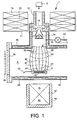
- electrically conductive elements 4 are of preferably metal studs comprising a zone containing at least one element such as iron, nickel, cobalt or any other metal or alloy having catalytic properties of fixation and dehydrogenation of non-condensable free radicals of the type CxHy °.
- each of the elements electrically conductive 4 is positioned on a electrical connection electrode 5.
- the device 1 comprises a deposition chamber 6, inside which is a substrate 8, preferably made of silicon, comprising an insulating layer 9, preferably made of SiO 2 . On this insulating layer 9 rest the electrodes 5 and a plurality of electrically conductive elements, including the two elements 4 intended to be connected.
- the filing chamber 6 is partially bounded by stainless steel structures to double wall 28,30, coupled with cooling 32,34.
- the device 1 comprises means injection 9 of a microwave power. Ways 9 are arranged in such a way that the microwaves are introduced into the device 1 of way to pass through a waveguide 10, then to pass through a window of tightness with microwaves 12, preferably quartz or alumina. The microwaves are then oriented towards the inside of the deposition chamber 6, preferably to limit the cost of the device at a frequency of approximately 2.45 GHz and at a power of about 500 W.
- the device 1 further comprises injection means 13,14 able to introduce into inside the deposition chamber 6 a gas containing carbon, these means 13,14 being notably constituted a gas supply pipe 14 and a valve leak 13.
- the carbon-containing gas is preferably selected from alkanes, alkenes, alkynes, and mixtures thereof. More In particular, we will use methane and acetylene.
- the gas injection means 13,14 are intended to operate injections at low pressure. It should be noted that low pressure means a pressure substantially less than about 3.10 -3 mbar, and preferably equal to about 8.10 -4 mbar.
- the device 1 comprises means 17,18 for creating a magnetic field to inside the deposit chamber 6, these means having a permanent magnet 17 located under the chamber deposition 6, as well as a permanent magnet housing 18.
- Ways to create the magnetic field also include magnetic field coils 19,20,21, located above the deposition chamber 6, surrounding the waveguide 10.
- the device 1 is also provided with at least an electronic cyclotron resonance zone 16, this last located inside the room of deposit 6, opposite substrate 8.
- the microwave power injection takes place at a frequency of 2.45 GHz, for a field value magnetic, corresponding to the cyclotron resonance electronic, of the order of 875 Gauss.
- the applied magnetic field in the deposition chamber 6 is of the mirror type magnetic strongly unbalanced.
- the magnetic field is maximum in the upper part of the chamber of deposit 6 at the level of the injection of microwave power. This same magnetic field is then minimum at level of the center of the filing room 6, then grows again when approaching the substrate 8.
- the magnetic field has a value of 2700 Gauss, while in the center of the room of deposit 6, the value of this magnetic field is about 500 Gauss.
- equimodule lines of magnetic field 44,45,46,47 are represented, the lines equimodules 44.45 representing the region of the depository chamber 6 in which the magnetic field has a value of 500 Gauss. Note that at the level of the resonance zone electronic cyclotron 16, a value of magnetic field of about 875 Gauss.
- the device 1 also includes a screen 22 delimiting a deposit zone 24, adjacent to the at least part of the substrate 8 comprising the two electrically conductive elements 4.
- a screen 22 delimiting a deposit zone 24, adjacent to the at least part of the substrate 8 comprising the two electrically conductive elements 4.
- the distance between the screen 22 and the substrate 8 is between approximately 0.1 and 10 mm.
- the screen 22 is a metal plate positioned substantially perpendicular to field lines 26 of the field magnetic applied.
- the plate metal 22 has an approximate form of rectangle, but can of course take any other form, according to the needs met.
- the substrate 8 is also placed substantially perpendicular to the lines of field 26 of the magnetic field applied inside the deposit chamber 6.
- the substrate 8 is heated by means of a filament 40 and a heating connection 42. This heating allows in particular to provide energy of activation necessary for the growth of the nanotube 2.
- the temperature of the substrate 2 is then between about 500 ° C and about 700 ° C.
- the device 1 is able to operate from the following way.
- non-condensable free radicals of the CxHy ° type are the species we want penetrate inside the deposit zone 24 of the device 1, in order to lead to the formation of quality nanotubes. For example, we can get solid nanotubes or single-walled nanotubes.
- the species produced following the ionization and / or dissociation of the carbon-containing gas there are in particular electrons and ions of the C + , C 2 + type , which are directly condensable species, capable of being deposited in all place.
- electrons and ions of the C + , C 2 + type which are directly condensable species, capable of being deposited in all place.
- non-condensable ions of the CxHy + type are in no case favorable to the growth of nanotubes and / or nanowires such as those which it is desired to obtain between the electrically conductive elements 4, the device 1 has been designed in order to prohibit these elements from accessing the deposition zone 24, in which the electrically conductive elements 4 to be connected are located.
- Ionized condensable species as well as the ionized non-condensable species cited above are magnetized, and thus diffuse from top to bottom in the deposition chamber 6, towards the substrate 8, the along the field lines 26 of the magnetic field applied. Note, as shown on the figure 2, that electrons wrap around field lines 26 following the Laplace force, and broadcast along these lines 26.
- the ionized species produced, of the C + , C 2 + , CxHy + type are deposited either on the screen plate 22, or on a part of the insulating layer 9 not being protected by this same plate 22 ( Figure 2).
- non-magnetized free radicals of the type CxHy ° circulate freely. at inside the deposit chamber 6, without being subjected to an imposed propagation direction. So, when they arrive near the screen plate 22, the lack of imposed direction allows them to penetrate inside the deposit zone 24, in which find the electrically conductive elements 4.
- non-selective carbon deposits generated by the condensable species of type C + , C 2 + , both on the screen plate 22 and on the part of the substrate 8 not protected by this same plate 22, are represented by the reference. 29 in Figure 2.
- non-condensable free radicals fix everything first on one of the two elements electrically conductors 4 to be connected, by establishing a connection carbon-metal. Once the fixing is done, it creates catalytic dehydrogenation of these compounds of the CxHy ° type.
- the carbon atoms in solution diffuse in and / or on the electrically conductive element 4 to precipitate and create a carbon nanotube 2, which then progresses towards the other element electrically conductive 4, while staying in touch of the substrate 8.
- nanotubes 2 can be more controlled by adding a gradient thermal, magnetic field or field in the deposit zone 24. Similarly, it is also possible to combine several elements supra.
- the invention also relates to a method for manufacturing at least one nanotube 2 connecting two electrically conductive elements 4, susceptible to be implemented by a device 1 such as that which has just been described.
- the electrically conductive elements 4 are located on a substrate 8.
- the method according to the invention implements microwave power in a deposition chamber 6, the latter being also subject to a field magnetic. Inside the deposition chamber 6, there is has an electronic cyclotron resonance zone 16, so that a low pressure introduction of a carbon-containing gas inside this chamber deposit 6 leads to ionization and / or dissociation of this gas in the cyclotron resonance zone electronic 16.
- the method further comprises a screening of the different species produced in the electronic cyclotron resonance zone 16. During this screening operation, only the non-condensable free radicals of the CxHy ° type are authorized to enter a deposit area 24, adjacent to at least part of the substrate 8 comprising the electrically conductive elements 4, to make the nanotube 2.
Landscapes
- Chemical & Material Sciences (AREA)
- Engineering & Computer Science (AREA)
- Physics & Mathematics (AREA)
- Materials Engineering (AREA)
- Nanotechnology (AREA)
- Organic Chemistry (AREA)
- Crystallography & Structural Chemistry (AREA)
- Metallurgy (AREA)
- Plasma & Fusion (AREA)
- General Chemical & Material Sciences (AREA)
- Chemical Kinetics & Catalysis (AREA)
- Condensed Matter Physics & Semiconductors (AREA)
- Inorganic Chemistry (AREA)
- General Physics & Mathematics (AREA)
- Analytical Chemistry (AREA)
- Mechanical Engineering (AREA)
- Mathematical Physics (AREA)
- Theoretical Computer Science (AREA)
- Spectroscopy & Molecular Physics (AREA)
- Electromagnetism (AREA)
- Manufacturing & Machinery (AREA)
- Composite Materials (AREA)
- Carbon And Carbon Compounds (AREA)
- Micromachines (AREA)
- Chemical Vapour Deposition (AREA)
Abstract
Description
- chauffage du substrat,
- mise en oeuvre de la puissance micro-ondes à l'intérieur de la chambre de dépôt,
- injection du gaz contenant du carbone,
- application du champ magnétique à l'intérieur de la chambre de dépôt, de façon à créer des lignes de champ sensiblement perpendiculaires au substrat et entraíner l'ionisation et/ou la dissociation du gaz dans la zone de résonance cyclotron électronique, de sorte que les ions et les électrons produits soient localisés sur les lignes de champ du champ magnétique,
- écrantage des espèces produites afin d'autoriser exclusivement aux radicaux libres non-condensables du type CxHy° l'accès à la zone de dépôt.
- une chambre de dépôt,
- des moyens d'injection d'une puissance micro-ondes à l'intérieur de la chambre de dépôt,
- des moyens permettant de créer un champ magnétique à l'intérieur de la chambre de dépôt,
- au moins une zone de résonance cyclotron électronique à l'intérieur de la chambre de dépôt.
- des moyens d'injection aptes à introduire à faible pression un gaz contenant du carbone, à l'intérieur de la chambre de dépôt,
- un écran délimitant une zone de dépôt adjacente à au moins une partie du substrat comprenant les deux éléments électriquement conducteurs et uniquement accessible aux radicaux libres non-condensables du type CxHy°.
- la figure 1 représente une vue schématique en coupe de face, d'un dispositif pour réaliser au moins un nanotube entre deux éléments électriquement conducteurs, selon un mode de réalisation préféré de l'invention, et
- la figure 2 représente une vue schématique, à plus grande échelle, d'une partie de la chambre de dépôt du dispositif de la figure 1.
- wHF : pulsation de l'onde haute fréquence injectée ;
- WCE : pulsation cyclotronique des électrons ;
- qe : charge de l'électron ;
- Br : champ de résonance ;
- me : masse de l'électron.
Claims (14)
- Procédé de fabrication d'au moins un nanotube (2) entre deux éléments électriquement conducteurs (4) situés sur un substrat (8), ledit procédé mettant en oeuvre, dans une chambre de dépôt (6), une puissance micro-ondes, un champ magnétique, ainsi qu'au moins une zone de résonance cyclotron électronique (16) favorisant l'ionisation et/ou la dissociation d'un gaz contenant du carbone injecté dans la chambre de dépôt (6),
caractérisé en ce que l'injection du gaz contenant du carbone est réalisée à faible pression à l'intérieur de la chambre de dépôt (6), entraínant l'ionisation et/ou la dissociation de ce gaz dans chaque zone de résonance cyclotron électronique (16), les ions et les électrons produits étant localisés sur les lignes de champ (26) du champ magnétique mis en oeuvre dans la chambre de dépôt (6),
le procédé comprenant en outre une opération d'écrantage des différentes espèces produites dans chaque zone de résonance cyclotron électronique (16), afin d'autoriser exclusivement aux radicaux libres non-condensables produits du type CxHy°, l'accès à une zone de dépôt (24) adjacente à au moins une partie du substrat (8) comprenant les deux éléments électriquement conducteurs (4), pour réaliser ledit nanotube (2). - Procédé selon la revendication 2, caractérisé en ce que l'opération d'écrantage est réalisée en interposant une plaque métallique (22) entre la zone de résonance cyclotron électronique (16) et les éléments électriquement conducteurs (4), ladite plaque métallique (22) étant sensiblement perpendiculaire aux lignes de champ (26) du champ magnétique appliqué dans la chambre de dépôt (6), de sorte que les ions et les électrons produits ne pénètrent pas dans la zone de dépôt (24).
- Procédé selon la revendication 1 ou la revendication 2, caractérisé en ce qu'une direction de croissance de chaque nanotube est favorisée par l'application, dans ladite zone de dépôt (24), d'au moins l'un des éléments pris parmi le groupe constitué d'un gradient thermique, d'un champ magnétique ou d'un champ électrique.
- Procédé selon l'une quelconque des revendications précédentes, caractérisé en ce qu'il comprend les étapes suivantes :chauffage du substrat (8),mise en oeuvre de la puissance micro-ondes à l'intérieur de la chambre de dépôt (6),injection du gaz contenant du carbone,application du champ magnétique à l'intérieur de la chambre de dépôt (6), de façon à créer des lignes de champ (26) sensiblement perpendiculaires audit substrat (8) et entraíner l'ionisation et/ou la dissociation du gaz dans chaque zone de résonance cyclotron électronique (16), de sorte que les ions et les électrons produits soient localisés sur les lignes de champ (26) dudit champ magnétique,écrantage des espèces produites afin d'autoriser exclusivement aux radicaux libres non-condensables du type CxHy° l'accès à ladite zone de dépôt (24).
- Procédé selon la revendication 4, caractérisé en ce que l'opération de chauffage du substrat (8) se réalise à une température comprise entre environ 500°C et environ 700°C.
- Procédé selon l'une quelconque des revendications précédentes, caractérisé en ce que la fréquence de la puissance micro-ondes mise en oeuvre dans la chambre de dépôt (6) est d'environ 2,45 GHz.
- Procédé selon l'une quelconque des revendications précédentes, caractérisé en ce que le gaz contenant du carbone est choisi parmi les alcanes, les alcènes, les alcynes, ainsi que leurs mélanges.
- Procédé selon l'une quelconque des revendications précédentes, caractérisé en ce que la faible pression d'injection du gaz contenant du carbone est inférieure à environ 3.10-3 mbar.
- Procédé selon l'une quelconque des revendications précédentes, caractérisé en ce que le champ magnétique appliqué dans la chambre de dépôt (6) est du type miroir magnétique fortement déséquilibré, le champ magnétique étant maximum à l'injection de la puissance micro-ondes, minimum au centre de la chambre de dépôt (6) et grandissant à nouveau en approchant du substrat (8).
- Procédé selon l'une quelconque des revendications précédentes, caractérisé en ce que les éléments électriquement conducteurs (4) comprennent au moins une zone contenant au moins un élément choisi parmi le fer, le nickel, le cobalt ou tout autre métal ou alliage ayant des propriétés catalytiques de fixation et de déshydrogénation des radicaux libres non-condensables du type CxHy°.
- Dispositif (1) pour réaliser au moins un nanotube (2) entre deux éléments électriquement conducteurs (4) se situant sur un substrat (8), ledit dispositif (1) comprenant :caractérisé en ce que le dispositif (1) comprend de plus :une chambre de dépôt (6),des moyens d'injection (9) d'une puissance micro-ondes à l'intérieur de la chambre de dépôt (6),des moyens (17,18,19,20,21) permettant de créer un champ magnétique à l'intérieur de la chambre de dépôt (6),au moins une zone de résonance cyclotron électronique (16) à l'intérieur de la chambre de dépôt (6),des moyens d'injection (13,14) aptes à introduire à faible pression un gaz contenant du carbone, à l'intérieur de la chambre de dépôt (6),un écran (22) délimitant une zone de dépôt (24) adjacente à au moins une partie du substrat (8) comprenant les deux éléments électriquement conducteurs (4) et uniquement accessible aux radicaux libres non-condensables du type CxHy°.
- Dispositif (1) selon la revendication 11, caractérisé en ce que l'écran (22) a une forme approximative de rectangle.
- Dispositif (1) selon la revendication 11 ou la revendication 12, caractérisé en ce que l'écran (22) est une plaque métallique positionnée sensiblement perpendiculairement aux lignes de champ (26) du champ magnétique, sur lesquelles sont localisées les ions et les électrons produits dans la zone de résonance cyclotron électronique (16).
- Dispositif (1) selon l'une quelconque des revendications 11 à 13, caractérisé en ce que le substrat (8) est sensiblement perpendiculairement aux lignes de champ (26) du champ magnétique appliqué à l'intérieur de la chambre de dépôt (6).
Applications Claiming Priority (2)
| Application Number | Priority Date | Filing Date | Title |
|---|---|---|---|
| FR0116871 | 2001-12-26 | ||
| FR0116871A FR2833935B1 (fr) | 2001-12-26 | 2001-12-26 | Procede de fabrication d'au moins un nanotube entre deux elements electriquement conducteurs et dispositif pour mettre en oeuvre un tel procede |
Publications (2)
| Publication Number | Publication Date |
|---|---|
| EP1323671A1 true EP1323671A1 (fr) | 2003-07-02 |
| EP1323671B1 EP1323671B1 (fr) | 2013-04-24 |
Family
ID=8870992
Family Applications (1)
| Application Number | Title | Priority Date | Filing Date |
|---|---|---|---|
| EP02293242.0A Expired - Lifetime EP1323671B1 (fr) | 2001-12-26 | 2002-12-24 | Procédé de fabrication d'au moins un nanotube entre deux éléments électriquement conducteurs et dispositif pour mettre en oeuvre un tel procédé |
Country Status (4)
| Country | Link |
|---|---|
| US (1) | US7160585B2 (fr) |
| EP (1) | EP1323671B1 (fr) |
| JP (1) | JP4064809B2 (fr) |
| FR (1) | FR2833935B1 (fr) |
Families Citing this family (8)
| Publication number | Priority date | Publication date | Assignee | Title |
|---|---|---|---|---|
| FR2815954B1 (fr) * | 2000-10-27 | 2003-02-21 | Commissariat Energie Atomique | Procede et dispositif de depot par plasma a la resonance cyclotron electronique de nanotubes de carbone monoparois et nanotubes ainsi obtenus |
| JP3969324B2 (ja) * | 2003-02-27 | 2007-09-05 | 富士ゼロックス株式会社 | カーボンナノチューブの製造装置 |
| JP2005213104A (ja) * | 2004-01-30 | 2005-08-11 | New Industry Research Organization | 高配向カーボンナノチューブの生成方法、及び高配向カーボンナノチューブの生成に適した装置。 |
| US7772125B2 (en) * | 2005-02-10 | 2010-08-10 | Panasonic Corporation | Structure in which cylindrical microstructure is maintained in anisotropic groove, method for fabricating the same, and semiconductor device, TFT driving circuit, panel, display and sensor using the structure in which cylindrical microstructure is maintained in anisotropic groove |
| JP5539210B2 (ja) * | 2007-10-02 | 2014-07-02 | プレジデント アンド フェローズ オブ ハーバード カレッジ | ナノポアデバイスのためのカーボンナノチューブ合成 |
| US9376321B2 (en) * | 2009-05-29 | 2016-06-28 | Postech Academy-Industry Foundation | Method and apparatus for manufacturing a nanowire |
| US9371232B2 (en) * | 2012-10-29 | 2016-06-21 | Bryan Edward Laubscher | Trekking atom nanotube growth |
| CN117800285B (zh) * | 2024-03-01 | 2024-05-17 | 浙江大学 | 一种环境气氛下多能场诱导原子级数控加工装置及方法 |
Citations (4)
| Publication number | Priority date | Publication date | Assignee | Title |
|---|---|---|---|---|
| EP0967844A1 (fr) * | 1998-06-24 | 1999-12-29 | Commissariat A L'energie Atomique | Procédé de dépÔt par plasma à la résonance cyclotron électronique de couches de carbone émetteur d'électrons sous l'effet d'un champ électrique appliqué |
| WO2001003158A1 (fr) * | 1999-07-01 | 2001-01-11 | Commissariat A L'energie Atomique | Procede et dispositif de depot par plasma a la resonance cyclotron electronique de couches de tissus de nanofibres de carbone et couches de tissus ainsi obtenus |
| WO2001044796A1 (fr) * | 1999-12-15 | 2001-06-21 | Board Of Trustees Of The Leland Stanford Junior University | Dispositifs de nanotubes de carbone |
| WO2002034669A1 (fr) * | 2000-10-27 | 2002-05-02 | Commissariat A L'energie Atomique | Procede et dispositif de depot par plasma a la resonance cyclotron electronique de nanotubes de carbone monoparois et nanotubes ainsi obtenus |
Family Cites Families (9)
| Publication number | Priority date | Publication date | Assignee | Title |
|---|---|---|---|---|
| EP0758028B1 (fr) * | 1995-07-10 | 2002-09-11 | Research Development Corporation Of Japan | Méthode pour produire des fibres de graphite |
| US6346189B1 (en) * | 1998-08-14 | 2002-02-12 | The Board Of Trustees Of The Leland Stanford Junior University | Carbon nanotube structures made using catalyst islands |
| TW452604B (en) * | 1999-01-11 | 2001-09-01 | Shih Han Jang | Process for synthesizing one-dimensional nanosubstances by electron cyclotron resonance chemical vapor deposition |
| US6420092B1 (en) * | 1999-07-14 | 2002-07-16 | Cheng-Jer Yang | Low dielectric constant nanotube |
| JP2001192829A (ja) * | 2000-01-05 | 2001-07-17 | Ulvac Japan Ltd | カーボンナノチューブ薄膜形成ecrプラズマcvd装置及び該薄膜の形成方法 |
| JP3595233B2 (ja) * | 2000-02-16 | 2004-12-02 | 株式会社ノリタケカンパニーリミテド | 電子放出源及びその製造方法 |
| JP4531193B2 (ja) * | 2000-04-10 | 2010-08-25 | 株式会社アルバック | スロットアンテナを用いたカーボンナノチューブ薄膜形成ecrプラズマcvd装置及び該薄膜の形成方法 |
| TW464896B (en) * | 2000-08-03 | 2001-11-21 | Nat Science Council | Method of manufacturing a field emitting display |
| JP3463091B2 (ja) * | 2000-08-29 | 2003-11-05 | 独立行政法人産業技術総合研究所 | カーボンナノチューブの製造方法 |
-
2001
- 2001-12-26 FR FR0116871A patent/FR2833935B1/fr not_active Expired - Fee Related
-
2002
- 2002-12-24 EP EP02293242.0A patent/EP1323671B1/fr not_active Expired - Lifetime
- 2002-12-24 JP JP2002373066A patent/JP4064809B2/ja not_active Expired - Fee Related
- 2002-12-26 US US10/330,618 patent/US7160585B2/en not_active Expired - Fee Related
Patent Citations (4)
| Publication number | Priority date | Publication date | Assignee | Title |
|---|---|---|---|---|
| EP0967844A1 (fr) * | 1998-06-24 | 1999-12-29 | Commissariat A L'energie Atomique | Procédé de dépÔt par plasma à la résonance cyclotron électronique de couches de carbone émetteur d'électrons sous l'effet d'un champ électrique appliqué |
| WO2001003158A1 (fr) * | 1999-07-01 | 2001-01-11 | Commissariat A L'energie Atomique | Procede et dispositif de depot par plasma a la resonance cyclotron electronique de couches de tissus de nanofibres de carbone et couches de tissus ainsi obtenus |
| WO2001044796A1 (fr) * | 1999-12-15 | 2001-06-21 | Board Of Trustees Of The Leland Stanford Junior University | Dispositifs de nanotubes de carbone |
| WO2002034669A1 (fr) * | 2000-10-27 | 2002-05-02 | Commissariat A L'energie Atomique | Procede et dispositif de depot par plasma a la resonance cyclotron electronique de nanotubes de carbone monoparois et nanotubes ainsi obtenus |
Non-Patent Citations (1)
| Title |
|---|
| TSAI S H ET AL: "Synthesis and characterization of the aligned hydrogenated amorphous carbon nanotubes by electron cyclotron resonance excitation", THIN SOLID FILMS, ELSEVIER-SEQUOIA S.A. LAUSANNE, CH, vol. 366, no. 1-2, May 2000 (2000-05-01), pages 11 - 15, XP004203828, ISSN: 0040-6090 * |
Also Published As
| Publication number | Publication date |
|---|---|
| FR2833935B1 (fr) | 2004-01-30 |
| US7160585B2 (en) | 2007-01-09 |
| FR2833935A1 (fr) | 2003-06-27 |
| JP2003261313A (ja) | 2003-09-16 |
| JP4064809B2 (ja) | 2008-03-19 |
| US20030173206A1 (en) | 2003-09-18 |
| EP1323671B1 (fr) | 2013-04-24 |
Similar Documents
| Publication | Publication Date | Title |
|---|---|---|
| EP1341718B1 (fr) | Procede et dispositif de depot par plasma a la resonance cyclotron electronique de nanotubes de carbone monoparois et nanotubes ainsi obtenus | |
| EP1451102B1 (fr) | PROCEDE DE CROISSANCE CATALYTIQUE DE NANOTUBES OU NANOFIBRES COMPRENANT UNE BARRIERE DE DIFFUSION DE TYPE ALLIAGE NiSi | |
| EP1614765B1 (fr) | Croissance à basse températurede nanotubes de carbone orientés | |
| EP2233435B1 (fr) | Procede d'elaboration de graphene | |
| EP1436823B1 (fr) | Procede de croissance localisee de nanotubes et procede de fabrication de cathode autoalignee utilisant le procede de croissance de nanotubes | |
| EP0944916B1 (fr) | Fils atomiques de grande longueur et de gande stabilite et procede de fabrication de ces fils | |
| EP1323671B1 (fr) | Procédé de fabrication d'au moins un nanotube entre deux éléments électriquement conducteurs et dispositif pour mettre en oeuvre un tel procédé | |
| FR2928939A1 (fr) | Procede de production de nanostructures sur un substrat d'oxyde metallique, procede de depot de couches minces sur un tel substrat, et un dispositf forme de couches minces | |
| FR2991100A1 (fr) | Transistor a base de nanofil, procede de fabrication du transistor, composant semi-conducteur integrant le transistor, programme informatique et support d'enregistrement associes au procede de fabrication | |
| EP3645460B1 (fr) | Procede de fabrication de nanotubes de carbone fixes sur un substrat | |
| CA2944274C (fr) | Procede et dispositif pour generer un plasma excite par une energie micro-onde dans le domaine de la resonnance cyclotronique electronique | |
| Pereira et al. | CH and CN Radical Contribution in the Particle Formation Generated in a Radio‐Frequency CH4/N2 Plasma | |
| EP2534678A1 (fr) | Structure d'interconnexion a base de nanotubes de carbone rediriges | |
| US7288490B1 (en) | Increased alignment in carbon nanotube growth | |
| FR2848204A1 (fr) | Procedes de synthese et de croissance de nanotiges d'un carbure metallique sur un substrat, substrats ainsi obtenus et leurs applications | |
| WO2014128250A1 (fr) | Procédé de fabrication d'un nanotube de carbone multi-parois; nanotube, source d'électrons et dispositif associés | |
| EP3267463A2 (fr) | Tube electronique sous vide a cathode planaire a base de nanotubes ou nanofils | |
| EP3568505B1 (fr) | Chambre de traitement pour un reacteur de depot chimique en phase vapeur (cvd) et procede de thermalisation mis en oeuvre dans cette chambre | |
| EP1971703A2 (fr) | Croissance catalytique et directionnelle de nanotubes de carbone individuels, application a des sources froides d'electrons | |
| FR2824002A1 (fr) | Procede de fabrication d'un reservoir a carburant faisant intervenir la decomposition d'un gaz de reaction sur l'enveloppe du reservoir | |
| Valappil et al. | Maximizing visible Raman resolution of nanodiamond grains fabricated by coaxial arc plasma deposition through oxygen plasma etching optimization | |
| EP3818189A1 (fr) | Procede et dispositif de synthese de diamant par cvd | |
| Mpingi | Structural, Electrical and Electronic Properties of Diamond like Carbon (DLC) and Carbon-Based Materials | |
| WO2022243418A1 (fr) | Procédé de préparation d'un composant microélectronique comprenant une couche à base d'un matériau iii-v | |
| FR2962590A1 (fr) | Cathode froide emettrice d'electrons a pointes renversees |
Legal Events
| Date | Code | Title | Description |
|---|---|---|---|
| PUAI | Public reference made under article 153(3) epc to a published international application that has entered the european phase |
Free format text: ORIGINAL CODE: 0009012 |
|
| AK | Designated contracting states |
Designated state(s): AT BE BG CH CY CZ DE DK EE ES FI FR GB GR IE IT LI LU MC NL PT SE SI SK TR |
|
| AX | Request for extension of the european patent |
Extension state: AL LT LV MK RO |
|
| 17P | Request for examination filed |
Effective date: 20031217 |
|
| AKX | Designation fees paid |
Designated state(s): AT BE BG CH CY CZ DE DK EE ES FI FR GB GR IE IT LI LU MC NL PT SE SI SK TR |
|
| 17Q | First examination report despatched |
Effective date: 20060929 |
|
| RAP1 | Party data changed (applicant data changed or rights of an application transferred) |
Owner name: COMMISSARIAT A L'ENERGIE ATOMIQUE |
|
| RAP1 | Party data changed (applicant data changed or rights of an application transferred) |
Owner name: COMMISSARIAT A L'ENERGIE ATOMIQUE ET AUX ENERGIES |
|
| REG | Reference to a national code |
Ref country code: DE Ref legal event code: R079 Ref document number: 60244856 Country of ref document: DE Free format text: PREVIOUS MAIN CLASS: C01B0031020000 Ipc: C23C0016260000 |
|
| GRAP | Despatch of communication of intention to grant a patent |
Free format text: ORIGINAL CODE: EPIDOSNIGR1 |
|
| RIC1 | Information provided on ipc code assigned before grant |
Ipc: C01B 31/02 20060101ALI20121016BHEP Ipc: B82Y 30/00 20110101ALI20121016BHEP Ipc: H01J 37/32 20060101ALI20121016BHEP Ipc: C23C 16/511 20060101ALI20121016BHEP Ipc: C23C 16/26 20060101AFI20121016BHEP Ipc: B82B 3/00 20060101ALI20121016BHEP Ipc: H05H 1/46 20060101ALI20121016BHEP Ipc: C30B 25/10 20060101ALI20121016BHEP Ipc: B82Y 10/00 20110101ALI20121016BHEP |
|
| GRAS | Grant fee paid |
Free format text: ORIGINAL CODE: EPIDOSNIGR3 |
|
| GRAA | (expected) grant |
Free format text: ORIGINAL CODE: 0009210 |
|
| AK | Designated contracting states |
Kind code of ref document: B1 Designated state(s): AT BE BG CH CY CZ DE DK EE ES FI FR GB GR IE IT LI LU MC NL PT SE SI SK TR |
|
| REG | Reference to a national code |
Ref country code: GB Ref legal event code: FG4D Free format text: NOT ENGLISH |
|
| REG | Reference to a national code |
Ref country code: CH Ref legal event code: EP |
|
| REG | Reference to a national code |
Ref country code: AT Ref legal event code: REF Ref document number: 608708 Country of ref document: AT Kind code of ref document: T Effective date: 20130515 |
|
| REG | Reference to a national code |
Ref country code: IE Ref legal event code: FG4D Free format text: LANGUAGE OF EP DOCUMENT: FRENCH |
|
| REG | Reference to a national code |
Ref country code: DE Ref legal event code: R096 Ref document number: 60244856 Country of ref document: DE Effective date: 20130620 |
|
| REG | Reference to a national code |
Ref country code: AT Ref legal event code: MK05 Ref document number: 608708 Country of ref document: AT Kind code of ref document: T Effective date: 20130424 |
|
| REG | Reference to a national code |
Ref country code: NL Ref legal event code: VDEP Effective date: 20130424 |
|
| PG25 | Lapsed in a contracting state [announced via postgrant information from national office to epo] |
Ref country code: FI Free format text: LAPSE BECAUSE OF FAILURE TO SUBMIT A TRANSLATION OF THE DESCRIPTION OR TO PAY THE FEE WITHIN THE PRESCRIBED TIME-LIMIT Effective date: 20130424 Ref country code: SI Free format text: LAPSE BECAUSE OF FAILURE TO SUBMIT A TRANSLATION OF THE DESCRIPTION OR TO PAY THE FEE WITHIN THE PRESCRIBED TIME-LIMIT Effective date: 20130424 Ref country code: PT Free format text: LAPSE BECAUSE OF FAILURE TO SUBMIT A TRANSLATION OF THE DESCRIPTION OR TO PAY THE FEE WITHIN THE PRESCRIBED TIME-LIMIT Effective date: 20130826 Ref country code: ES Free format text: LAPSE BECAUSE OF FAILURE TO SUBMIT A TRANSLATION OF THE DESCRIPTION OR TO PAY THE FEE WITHIN THE PRESCRIBED TIME-LIMIT Effective date: 20130804 Ref country code: GR Free format text: LAPSE BECAUSE OF FAILURE TO SUBMIT A TRANSLATION OF THE DESCRIPTION OR TO PAY THE FEE WITHIN THE PRESCRIBED TIME-LIMIT Effective date: 20130725 Ref country code: SE Free format text: LAPSE BECAUSE OF FAILURE TO SUBMIT A TRANSLATION OF THE DESCRIPTION OR TO PAY THE FEE WITHIN THE PRESCRIBED TIME-LIMIT Effective date: 20130424 Ref country code: AT Free format text: LAPSE BECAUSE OF FAILURE TO SUBMIT A TRANSLATION OF THE DESCRIPTION OR TO PAY THE FEE WITHIN THE PRESCRIBED TIME-LIMIT Effective date: 20130424 |
|
| PG25 | Lapsed in a contracting state [announced via postgrant information from national office to epo] |
Ref country code: CY Free format text: LAPSE BECAUSE OF FAILURE TO SUBMIT A TRANSLATION OF THE DESCRIPTION OR TO PAY THE FEE WITHIN THE PRESCRIBED TIME-LIMIT Effective date: 20130424 Ref country code: BG Free format text: LAPSE BECAUSE OF FAILURE TO SUBMIT A TRANSLATION OF THE DESCRIPTION OR TO PAY THE FEE WITHIN THE PRESCRIBED TIME-LIMIT Effective date: 20130724 |
|
| PG25 | Lapsed in a contracting state [announced via postgrant information from national office to epo] |
Ref country code: EE Free format text: LAPSE BECAUSE OF FAILURE TO SUBMIT A TRANSLATION OF THE DESCRIPTION OR TO PAY THE FEE WITHIN THE PRESCRIBED TIME-LIMIT Effective date: 20130424 Ref country code: CZ Free format text: LAPSE BECAUSE OF FAILURE TO SUBMIT A TRANSLATION OF THE DESCRIPTION OR TO PAY THE FEE WITHIN THE PRESCRIBED TIME-LIMIT Effective date: 20130424 Ref country code: SK Free format text: LAPSE BECAUSE OF FAILURE TO SUBMIT A TRANSLATION OF THE DESCRIPTION OR TO PAY THE FEE WITHIN THE PRESCRIBED TIME-LIMIT Effective date: 20130424 Ref country code: DK Free format text: LAPSE BECAUSE OF FAILURE TO SUBMIT A TRANSLATION OF THE DESCRIPTION OR TO PAY THE FEE WITHIN THE PRESCRIBED TIME-LIMIT Effective date: 20130424 |
|
| PG25 | Lapsed in a contracting state [announced via postgrant information from national office to epo] |
Ref country code: IT Free format text: LAPSE BECAUSE OF FAILURE TO SUBMIT A TRANSLATION OF THE DESCRIPTION OR TO PAY THE FEE WITHIN THE PRESCRIBED TIME-LIMIT Effective date: 20130424 Ref country code: NL Free format text: LAPSE BECAUSE OF FAILURE TO SUBMIT A TRANSLATION OF THE DESCRIPTION OR TO PAY THE FEE WITHIN THE PRESCRIBED TIME-LIMIT Effective date: 20130424 |
|
| PLBE | No opposition filed within time limit |
Free format text: ORIGINAL CODE: 0009261 |
|
| STAA | Information on the status of an ep patent application or granted ep patent |
Free format text: STATUS: NO OPPOSITION FILED WITHIN TIME LIMIT |
|
| 26N | No opposition filed |
Effective date: 20140127 |
|
| REG | Reference to a national code |
Ref country code: DE Ref legal event code: R097 Ref document number: 60244856 Country of ref document: DE Effective date: 20140127 |
|
| BERE | Be: lapsed |
Owner name: COMMISSARIAT A L'ENERGIE ATOMIQUE ET AUX ENERGIES Effective date: 20131231 |
|
| REG | Reference to a national code |
Ref country code: CH Ref legal event code: PL |
|
| PG25 | Lapsed in a contracting state [announced via postgrant information from national office to epo] |
Ref country code: MC Free format text: LAPSE BECAUSE OF FAILURE TO SUBMIT A TRANSLATION OF THE DESCRIPTION OR TO PAY THE FEE WITHIN THE PRESCRIBED TIME-LIMIT Effective date: 20130424 Ref country code: LU Free format text: LAPSE BECAUSE OF FAILURE TO SUBMIT A TRANSLATION OF THE DESCRIPTION OR TO PAY THE FEE WITHIN THE PRESCRIBED TIME-LIMIT Effective date: 20131224 |
|
| REG | Reference to a national code |
Ref country code: IE Ref legal event code: MM4A |
|
| PG25 | Lapsed in a contracting state [announced via postgrant information from national office to epo] |
Ref country code: LI Free format text: LAPSE BECAUSE OF NON-PAYMENT OF DUE FEES Effective date: 20131231 Ref country code: BE Free format text: LAPSE BECAUSE OF NON-PAYMENT OF DUE FEES Effective date: 20131231 Ref country code: CH Free format text: LAPSE BECAUSE OF NON-PAYMENT OF DUE FEES Effective date: 20131231 Ref country code: IE Free format text: LAPSE BECAUSE OF NON-PAYMENT OF DUE FEES Effective date: 20131224 |
|
| PGFP | Annual fee paid to national office [announced via postgrant information from national office to epo] |
Ref country code: GB Payment date: 20141218 Year of fee payment: 13 |
|
| PGFP | Annual fee paid to national office [announced via postgrant information from national office to epo] |
Ref country code: DE Payment date: 20141211 Year of fee payment: 13 |
|
| PGFP | Annual fee paid to national office [announced via postgrant information from national office to epo] |
Ref country code: FR Payment date: 20141231 Year of fee payment: 13 |
|
| PG25 | Lapsed in a contracting state [announced via postgrant information from national office to epo] |
Ref country code: TR Free format text: LAPSE BECAUSE OF FAILURE TO SUBMIT A TRANSLATION OF THE DESCRIPTION OR TO PAY THE FEE WITHIN THE PRESCRIBED TIME-LIMIT Effective date: 20130424 |
|
| REG | Reference to a national code |
Ref country code: DE Ref legal event code: R119 Ref document number: 60244856 Country of ref document: DE |
|
| GBPC | Gb: european patent ceased through non-payment of renewal fee |
Effective date: 20151224 |
|
| REG | Reference to a national code |
Ref country code: FR Ref legal event code: ST Effective date: 20160831 |
|
| PG25 | Lapsed in a contracting state [announced via postgrant information from national office to epo] |
Ref country code: GB Free format text: LAPSE BECAUSE OF NON-PAYMENT OF DUE FEES Effective date: 20151224 Ref country code: DE Free format text: LAPSE BECAUSE OF NON-PAYMENT OF DUE FEES Effective date: 20160701 |
|
| PG25 | Lapsed in a contracting state [announced via postgrant information from national office to epo] |
Ref country code: FR Free format text: LAPSE BECAUSE OF NON-PAYMENT OF DUE FEES Effective date: 20151231 |