EP1323466A1 - Procédé de dépôt sélectif de matière sur des électrodes de biocapteurs ou de puces réalisés à partir d'un même substrat - Google Patents
Procédé de dépôt sélectif de matière sur des électrodes de biocapteurs ou de puces réalisés à partir d'un même substrat Download PDFInfo
- Publication number
- EP1323466A1 EP1323466A1 EP02293241A EP02293241A EP1323466A1 EP 1323466 A1 EP1323466 A1 EP 1323466A1 EP 02293241 A EP02293241 A EP 02293241A EP 02293241 A EP02293241 A EP 02293241A EP 1323466 A1 EP1323466 A1 EP 1323466A1
- Authority
- EP
- European Patent Office
- Prior art keywords
- electrodes
- address
- chips
- biosensors
- biosensor
- Prior art date
- Legal status (The legal status is an assumption and is not a legal conclusion. Google has not performed a legal analysis and makes no representation as to the accuracy of the status listed.)
- Granted
Links
- 239000000758 substrate Substances 0.000 title claims abstract description 27
- 238000000034 method Methods 0.000 title claims abstract description 25
- 239000000463 material Substances 0.000 title claims abstract description 18
- 230000008021 deposition Effects 0.000 title claims abstract description 7
- 230000008569 process Effects 0.000 title claims description 9
- 238000000151 deposition Methods 0.000 claims abstract description 10
- 230000004913 activation Effects 0.000 claims abstract description 8
- 238000009713 electroplating Methods 0.000 claims description 3
- 230000010287 polarization Effects 0.000 claims description 3
- 239000000126 substance Substances 0.000 claims description 3
- 238000004070 electrodeposition Methods 0.000 abstract description 3
- 230000003213 activating effect Effects 0.000 abstract 1
- 238000007306 functionalization reaction Methods 0.000 description 8
- 239000003153 chemical reaction reagent Substances 0.000 description 7
- 239000004065 semiconductor Substances 0.000 description 4
- 239000013626 chemical specie Substances 0.000 description 2
- 238000007334 copolymerization reaction Methods 0.000 description 2
- 238000004519 manufacturing process Methods 0.000 description 2
- 238000004377 microelectronic Methods 0.000 description 2
- 238000000018 DNA microarray Methods 0.000 description 1
- 238000004458 analytical method Methods 0.000 description 1
- 238000012742 biochemical analysis Methods 0.000 description 1
- 230000015572 biosynthetic process Effects 0.000 description 1
- 230000000295 complement effect Effects 0.000 description 1
- 229920001940 conductive polymer Polymers 0.000 description 1
- 238000007796 conventional method Methods 0.000 description 1
- 238000005137 deposition process Methods 0.000 description 1
- 230000006872 improvement Effects 0.000 description 1
- 238000001465 metallisation Methods 0.000 description 1
- 230000004048 modification Effects 0.000 description 1
- 238000012986 modification Methods 0.000 description 1
Images


Classifications
-
- B—PERFORMING OPERATIONS; TRANSPORTING
- B01—PHYSICAL OR CHEMICAL PROCESSES OR APPARATUS IN GENERAL
- B01J—CHEMICAL OR PHYSICAL PROCESSES, e.g. CATALYSIS OR COLLOID CHEMISTRY; THEIR RELEVANT APPARATUS
- B01J19/00—Chemical, physical or physico-chemical processes in general; Their relevant apparatus
- B01J19/0046—Sequential or parallel reactions, e.g. for the synthesis of polypeptides or polynucleotides; Apparatus and devices for combinatorial chemistry or for making molecular arrays
-
- B—PERFORMING OPERATIONS; TRANSPORTING
- B01—PHYSICAL OR CHEMICAL PROCESSES OR APPARATUS IN GENERAL
- B01J—CHEMICAL OR PHYSICAL PROCESSES, e.g. CATALYSIS OR COLLOID CHEMISTRY; THEIR RELEVANT APPARATUS
- B01J2219/00—Chemical, physical or physico-chemical processes in general; Their relevant apparatus
- B01J2219/00274—Sequential or parallel reactions; Apparatus and devices for combinatorial chemistry or for making arrays; Chemical library technology
- B01J2219/00277—Apparatus
- B01J2219/0054—Means for coding or tagging the apparatus or the reagents
- B01J2219/00565—Electromagnetic means
-
- B—PERFORMING OPERATIONS; TRANSPORTING
- B01—PHYSICAL OR CHEMICAL PROCESSES OR APPARATUS IN GENERAL
- B01J—CHEMICAL OR PHYSICAL PROCESSES, e.g. CATALYSIS OR COLLOID CHEMISTRY; THEIR RELEVANT APPARATUS
- B01J2219/00—Chemical, physical or physico-chemical processes in general; Their relevant apparatus
- B01J2219/00274—Sequential or parallel reactions; Apparatus and devices for combinatorial chemistry or for making arrays; Chemical library technology
- B01J2219/00583—Features relative to the processes being carried out
- B01J2219/00585—Parallel processes
-
- B—PERFORMING OPERATIONS; TRANSPORTING
- B01—PHYSICAL OR CHEMICAL PROCESSES OR APPARATUS IN GENERAL
- B01J—CHEMICAL OR PHYSICAL PROCESSES, e.g. CATALYSIS OR COLLOID CHEMISTRY; THEIR RELEVANT APPARATUS
- B01J2219/00—Chemical, physical or physico-chemical processes in general; Their relevant apparatus
- B01J2219/00274—Sequential or parallel reactions; Apparatus and devices for combinatorial chemistry or for making arrays; Chemical library technology
- B01J2219/00583—Features relative to the processes being carried out
- B01J2219/0059—Sequential processes
-
- B—PERFORMING OPERATIONS; TRANSPORTING
- B01—PHYSICAL OR CHEMICAL PROCESSES OR APPARATUS IN GENERAL
- B01J—CHEMICAL OR PHYSICAL PROCESSES, e.g. CATALYSIS OR COLLOID CHEMISTRY; THEIR RELEVANT APPARATUS
- B01J2219/00—Chemical, physical or physico-chemical processes in general; Their relevant apparatus
- B01J2219/00274—Sequential or parallel reactions; Apparatus and devices for combinatorial chemistry or for making arrays; Chemical library technology
- B01J2219/00583—Features relative to the processes being carried out
- B01J2219/00596—Solid-phase processes
-
- B—PERFORMING OPERATIONS; TRANSPORTING
- B01—PHYSICAL OR CHEMICAL PROCESSES OR APPARATUS IN GENERAL
- B01J—CHEMICAL OR PHYSICAL PROCESSES, e.g. CATALYSIS OR COLLOID CHEMISTRY; THEIR RELEVANT APPARATUS
- B01J2219/00—Chemical, physical or physico-chemical processes in general; Their relevant apparatus
- B01J2219/00274—Sequential or parallel reactions; Apparatus and devices for combinatorial chemistry or for making arrays; Chemical library technology
- B01J2219/00583—Features relative to the processes being carried out
- B01J2219/00603—Making arrays on substantially continuous surfaces
- B01J2219/00605—Making arrays on substantially continuous surfaces the compounds being directly bound or immobilised to solid supports
-
- B—PERFORMING OPERATIONS; TRANSPORTING
- B01—PHYSICAL OR CHEMICAL PROCESSES OR APPARATUS IN GENERAL
- B01J—CHEMICAL OR PHYSICAL PROCESSES, e.g. CATALYSIS OR COLLOID CHEMISTRY; THEIR RELEVANT APPARATUS
- B01J2219/00—Chemical, physical or physico-chemical processes in general; Their relevant apparatus
- B01J2219/00274—Sequential or parallel reactions; Apparatus and devices for combinatorial chemistry or for making arrays; Chemical library technology
- B01J2219/00583—Features relative to the processes being carried out
- B01J2219/00603—Making arrays on substantially continuous surfaces
- B01J2219/00653—Making arrays on substantially continuous surfaces the compounds being bound to electrodes embedded in or on the solid supports
-
- B—PERFORMING OPERATIONS; TRANSPORTING
- B01—PHYSICAL OR CHEMICAL PROCESSES OR APPARATUS IN GENERAL
- B01J—CHEMICAL OR PHYSICAL PROCESSES, e.g. CATALYSIS OR COLLOID CHEMISTRY; THEIR RELEVANT APPARATUS
- B01J2219/00—Chemical, physical or physico-chemical processes in general; Their relevant apparatus
- B01J2219/00274—Sequential or parallel reactions; Apparatus and devices for combinatorial chemistry or for making arrays; Chemical library technology
- B01J2219/00583—Features relative to the processes being carried out
- B01J2219/00603—Making arrays on substantially continuous surfaces
- B01J2219/00659—Two-dimensional arrays
-
- B—PERFORMING OPERATIONS; TRANSPORTING
- B01—PHYSICAL OR CHEMICAL PROCESSES OR APPARATUS IN GENERAL
- B01J—CHEMICAL OR PHYSICAL PROCESSES, e.g. CATALYSIS OR COLLOID CHEMISTRY; THEIR RELEVANT APPARATUS
- B01J2219/00—Chemical, physical or physico-chemical processes in general; Their relevant apparatus
- B01J2219/00274—Sequential or parallel reactions; Apparatus and devices for combinatorial chemistry or for making arrays; Chemical library technology
- B01J2219/00583—Features relative to the processes being carried out
- B01J2219/00603—Making arrays on substantially continuous surfaces
- B01J2219/00659—Two-dimensional arrays
- B01J2219/00662—Two-dimensional arrays within two-dimensional arrays
-
- B—PERFORMING OPERATIONS; TRANSPORTING
- B01—PHYSICAL OR CHEMICAL PROCESSES OR APPARATUS IN GENERAL
- B01J—CHEMICAL OR PHYSICAL PROCESSES, e.g. CATALYSIS OR COLLOID CHEMISTRY; THEIR RELEVANT APPARATUS
- B01J2219/00—Chemical, physical or physico-chemical processes in general; Their relevant apparatus
- B01J2219/00274—Sequential or parallel reactions; Apparatus and devices for combinatorial chemistry or for making arrays; Chemical library technology
- B01J2219/0068—Means for controlling the apparatus of the process
- B01J2219/00686—Automatic
- B01J2219/00689—Automatic using computers
-
- B—PERFORMING OPERATIONS; TRANSPORTING
- B01—PHYSICAL OR CHEMICAL PROCESSES OR APPARATUS IN GENERAL
- B01J—CHEMICAL OR PHYSICAL PROCESSES, e.g. CATALYSIS OR COLLOID CHEMISTRY; THEIR RELEVANT APPARATUS
- B01J2219/00—Chemical, physical or physico-chemical processes in general; Their relevant apparatus
- B01J2219/00274—Sequential or parallel reactions; Apparatus and devices for combinatorial chemistry or for making arrays; Chemical library technology
- B01J2219/00709—Type of synthesis
- B01J2219/00713—Electrochemical synthesis
-
- B—PERFORMING OPERATIONS; TRANSPORTING
- B01—PHYSICAL OR CHEMICAL PROCESSES OR APPARATUS IN GENERAL
- B01J—CHEMICAL OR PHYSICAL PROCESSES, e.g. CATALYSIS OR COLLOID CHEMISTRY; THEIR RELEVANT APPARATUS
- B01J2219/00—Chemical, physical or physico-chemical processes in general; Their relevant apparatus
- B01J2219/00274—Sequential or parallel reactions; Apparatus and devices for combinatorial chemistry or for making arrays; Chemical library technology
- B01J2219/00718—Type of compounds synthesised
- B01J2219/0072—Organic compounds
-
- C—CHEMISTRY; METALLURGY
- C40—COMBINATORIAL TECHNOLOGY
- C40B—COMBINATORIAL CHEMISTRY; LIBRARIES, e.g. CHEMICAL LIBRARIES
- C40B70/00—Tags or labels specially adapted for combinatorial chemistry or libraries, e.g. fluorescent tags or bar codes
Definitions
- the invention relates to a method of selective deposition of material on electrodes of biosensors or chips made from the same substrate. It concerns in particular devices of microelectronics with several elements interconnected on the same starting board or substrate.
- micro-systems which, in the field of biological or biochemical analysis or more generally pharmacology tests, allow the analysis of a very large number of points by methods of collective binding of reagents on a multizone plan.
- micro-systems can be made by "biochips" which are chips having a part of the electrical circuit realized on a substrate (an electrode field for example) and a biological part made on the surface of the chips.
- One of the techniques used to fix these reagents is the electrodeposition on sites electrically polarized conductive polymer carrier of the chosen chemical or biological species as a reagent.
- the substrate is electrically connected outward and is soaked in a tank containing a solution carrying the chemical species or biological deposit.
- the chosen site is polarized and the copolymerization takes place. Then we go to a another solution carrying another reagent.
- Another site is polarized for further copolymerization.
- the cycle is repeated as many times as there are reagents different to fix.
- An interesting improvement is to integrate the addressing electronics of the sites into the substrate itself. This technique is sequential. Each site is successively polarized and the substrate is soaked in the carrier solution of the reagent to each pass.
- FR-A-2,741,476 discloses the application of the method to a wafer (or substrate) intended to provide a plurality of chips, which is already a very big progress for the time of functionalization of the sites.
- the treatment of a wafer, to obtain a plurality of chips can involve different technics.
- fleas can to be carried out according to a photorepetition process, then the assembly can be carried out according to a method full slice. It is also possible to achieve by a process in full slice.
- the present invention makes it possible to remedy these disadvantages.
- the electrical connection means of the substrate to connect the address pads can understand repeaters.
- the deposited material may consist of species chemical, biochemical or biological.
- the invention allows individual addressing of each of the biosensors or chips made on a semiconductor wafer in order to get a more great flexibility of use when functionalization, ranging from the treatment of all biosensors or all chips of the wafer in parallel to the individual treatment of each biosensor or each chip. More precisely, the invention is to use the principle of the deposit electrochemical at the platelet scale, with individual addressing of each of the biosensors or each of the chips of the wafer by programming of the address of each biosensor or each chip and decoding the addresses inside the command word transmitted in parallel on all biosensors or on all the chips of the wafer.
- the programming of the address can also to be carried out in several levels.
- the biosensors or chips are assembled in a field photorepetition, it is possible to have a programming inside the field, by levels conventional, low-order bits of the address and programming of the most significant bits at the level of the plate in full slice level. It is possible also to program all address bits into one full level slice by the last level of metallization full slice for example. Only one level is then sufficient to program the address of the biosensor or chip and this programming can be visually readable in the manner of a barcode, on the biosensor or functionalized chip.
- each biosensor or each chip can be activated individually and remain active during activation other biosensors or other chips. Then inside each biosensor or activated chip, each of the electrodes can be individually connected to the external source (potentiostat) and therefore to be determined as a reagent hooking site.
- the external source potentiostat
- the treatment of a substrate to form biosensors or chips, including their addressing, is identical to the treatment disclosed in the document FR-A-2 741 476 cited above, the programming being realized during the formation of the biosensor network or chips.
- One or more substrates are first made on a substrate several sets of biosensors or chips identical, each comprising a plurality of electrodes and having non-address pins connected. This achievement is made following any conventional method of manufacturing microelectronic devices.
- each address bit is connected for each biosensor or chip according to a code constituting the programming the address of the biosensor or the chip.
- the repeater circuit is an additional circuit which allows the redistribution of orders distributed on all the biosensors or on all the chips and the concentration of an output by biosensor or chip in a single common exit. In the case of a making biosensors or chips by photorepetition, it is possible to provide a repeater by photorepetition field.
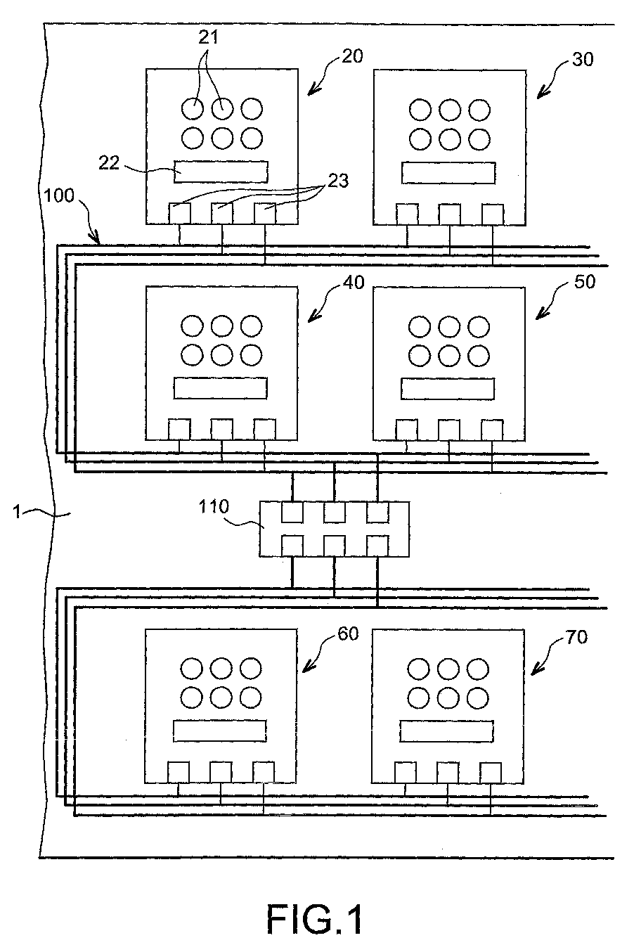
- FIG. 1 shows part of a substrate semiconductor 1 on which some biosensors or chips 20, 30, 40, 50, 60 and 70 are visible.
- Each biosensor or chip is equipped with a plurality electrodes, for example the electrodes 21 for the biosensor or chip 20.
- Each biosensor or chip is provided with a zone of address, for example the zone address 22 for the biosensor or for the chip 20, containing the programmed address of the biosensor or the chip.
- Each biosensor or chip is also provided interconnection pads, for example studs interconnections 23 for the biosensor or chip 20.
- biosensors or chips can use any process electrodeposition.
- the operation is then carried out electrodes on the connected electrodes of biosensors or activated chips, by a method of known art.
- the address of the biosensor or chip to activate is contained in the activation command. This command is sent to all biosensors or chips from the wafer and the address is decoded by each of the biosensors or each of the chips.
- the number of bits needed to address a biosensor or a chip in all the wafer depends on the size of the biosensor or chip and wafer used. For example, 7 address bits allow to address 128 biosensors or chips.
- Figure 2 illustrates the operation of programming a biosensor or chip to a address given by the direct connection method.
- the decoding circuit 2 receives as input a word of M command and outputs the decoded address on pads 3 (from A0 to A6b).
- Each of the address pads 4 biosensor or chip (from a0 to a6) is connected to the corresponding block in the decoded addresses or its complement.
- the pads 4 then provide (in the case of Figure 2) address 0100110 at the circuit of use 5.
- Figure 3 illustrates the operation of programming a biosensor or chip to a address given by the comparison method.
- the decoding circuit 12 receives as input a word of M command and outputs the decoded address to first inputs of a comparison circuit 16.
- Each of the address pads 14 of the biosensor or the chip (from a0 to a6) is connected to second inputs of the comparison circuit 16.
- the address pads 14 are at a high or low potential depending on the coding.
- the biosensor or chip is programmed at 0100110.
- the address of the biosensor or chip is compared to the decoded address in the command word.
- the output of the comparison circuit 16 is connected to the utilization circuit 15.
- the invention leaves the possibility of limiting at will the number of biosensors or chips activated at each passage. This provides extreme flexibility in final configuration of the various sites of the wafer.
- a biosensor or chip alone can be addressed and enabled for connection of its electrodes.
- a number of biosensors or chips can be activated one or one after the other, or all the biosensors or all the chips of the substrate and the operation electroplating can be performed on all biosensors or on all activated chips.
- the invention allows all possible configurations, between a parallelization complete for a treatment of all biosensors or of all the substrate chips and a treatment individual of each biosensor or each chip.
Landscapes
- Chemical & Material Sciences (AREA)
- Organic Chemistry (AREA)
- Chemical Kinetics & Catalysis (AREA)
- Apparatus Associated With Microorganisms And Enzymes (AREA)
- Electrodes Of Semiconductors (AREA)
- Investigating Or Analyzing Materials By The Use Of Electric Means (AREA)
- Electroplating Methods And Accessories (AREA)
- Measuring Or Testing Involving Enzymes Or Micro-Organisms (AREA)
Abstract
Description
- l'envoi successif sur les plots d'adresse des biocapteurs ou des puces à activer de mots de commande appropriés pour les activer successivement, la reconnaissance par lesdits biocapteurs ou lesdites puces des mots de commande appropriés déterminant leur placement à l'état activé,
- la connexion des électrodes devant recevoir le dépôt de ladite première matière à des moyens de polarisation par adressage de ces électrodes,
- la figure 1 montre un certain nombre de puces réalisées sur un substrat semiconducteur conformément à l'invention,
- la figure 2 illustre l'opération de programmation d'une puce à une adresse donnée par la méthode de connexion directe,
- la figure 3 illustre l'opération de programmation d'un biocapteur ou d'une puce à une adresse donnée par la méthode par comparaison.
Claims (3)
- Procédé de dépôt sélectif de matière sur des électrodes (21) de biocapteurs ou de puces (20) réalisés à partir d'un même substrat (1), caractérisé en ce qu'il comprend les étapes de :a) réalisation sur ledit substrat (1) d'une pluralité de biocapteur ou de puces (20, 30, 40, 50, 60, 70), chaque biocapteur ou chaque puce comprenant une pluralité d'électrodes (21) sur lesquelles des dépôts sélectifs de matière doivent être réalisés, des plots d'adresse (23), une zone d'adresse (22) contenant l'adresse programmée du biocapteur ou de la puce, connectée aux plots d'adresse et apte à reconnaítre l'adresse dudit biocapteur ou de ladite puce pour le/la placer dans un état dit activé si l'adresse du biocapteur ou de la puce contenue dans un mot de commande reçu sur les plots d'adresse est exacte, le substrat comportant également des moyens de liaisons électriques (100) permettant de connecter les plots d'adresse (23) et la pluralité d'électrodes (21) de chaque biocapteur ou de chaque puce vers des moyens d'adressage permettant l'activation des biocapteurs ou des puces et la polarisation des électrodes,b) adressage des biocapteurs ou des puces et des électrodes sur lesquelles le dépôt d'une première matière doit être réalisé comprenant :l'envoi successif sur les plots d'adresse (23) des biocapteurs ou des puces (20) à activer de mots de commande appropriés pour les activer successivement, la reconnaissance par lesdits biocapteurs ou lesdites puces des mots de commande appropriés déterminant leur placement à l'état activé,la connexion des électrodes devant recevoir le dépôt de ladite première matière à des moyens de polarisation par adressage de ces électrodes,c) le dépôt de ladite première matière simultanément sur les électrodes concernées par électrodéposition,d) le renouvellement des étapes b) et c) autant de fois que nécessaire pour effectuer des dépôts de matière sur les autres électrodes.
- Procédé selon la revendication 1, caractérisé en ce que les moyens de liaisons électriques du substrat permettant de connecter les plots d'adresse comprennent des répéteurs (110).
- Procédé selon l'une quelconque des revendications 1 ou 2, caractérisé en ce que la matière déposée est constituée d'espèces chimiques, biochimiques ou biologiques.
Applications Claiming Priority (2)
| Application Number | Priority Date | Filing Date | Title |
|---|---|---|---|
| FR0116922A FR2834383B1 (fr) | 2001-12-27 | 2001-12-27 | Procede de depot selectif de matiere sur des electrodes de biocapteurs ou de puces realises a partir d'un meme substrat |
| FR0116922 | 2001-12-27 |
Publications (2)
| Publication Number | Publication Date |
|---|---|
| EP1323466A1 true EP1323466A1 (fr) | 2003-07-02 |
| EP1323466B1 EP1323466B1 (fr) | 2011-09-28 |
Family
ID=8871020
Family Applications (1)
| Application Number | Title | Priority Date | Filing Date |
|---|---|---|---|
| EP02293241A Expired - Lifetime EP1323466B1 (fr) | 2001-12-27 | 2002-12-24 | Procédé de dépôt sélectif de matière sur des électrodes de biocapteurs ou de puces réalisés à partir d'un même substrat |
Country Status (5)
| Country | Link |
|---|---|
| US (1) | US6852552B2 (fr) |
| EP (1) | EP1323466B1 (fr) |
| JP (1) | JP4101640B2 (fr) |
| AT (1) | ATE526078T1 (fr) |
| FR (1) | FR2834383B1 (fr) |
Families Citing this family (2)
| Publication number | Priority date | Publication date | Assignee | Title |
|---|---|---|---|---|
| FR2834383B1 (fr) * | 2001-12-27 | 2004-02-13 | Commissariat Energie Atomique | Procede de depot selectif de matiere sur des electrodes de biocapteurs ou de puces realises a partir d'un meme substrat |
| JP4774980B2 (ja) * | 2005-12-21 | 2011-09-21 | 凸版印刷株式会社 | Dnaチップ装置 |
Citations (3)
| Publication number | Priority date | Publication date | Assignee | Title |
|---|---|---|---|---|
| FR2741476A1 (fr) * | 1995-11-17 | 1997-05-23 | Commissariat Energie Atomique | Procede de realisation collective de puces avec des electrodes selectivement recouvertes par un depot |
| WO1998001221A1 (fr) * | 1996-07-05 | 1998-01-15 | Combimatrix Corporation | Synthese electrochimique de polymeres en phase solide |
| US6251595B1 (en) * | 1998-06-18 | 2001-06-26 | Agilent Technologies, Inc. | Methods and devices for carrying out chemical reactions |
Family Cites Families (1)
| Publication number | Priority date | Publication date | Assignee | Title |
|---|---|---|---|---|
| FR2834383B1 (fr) * | 2001-12-27 | 2004-02-13 | Commissariat Energie Atomique | Procede de depot selectif de matiere sur des electrodes de biocapteurs ou de puces realises a partir d'un meme substrat |
-
2001
- 2001-12-27 FR FR0116922A patent/FR2834383B1/fr not_active Expired - Fee Related
-
2002
- 2002-12-17 US US10/320,690 patent/US6852552B2/en not_active Expired - Fee Related
- 2002-12-24 AT AT02293241T patent/ATE526078T1/de not_active IP Right Cessation
- 2002-12-24 JP JP2002373067A patent/JP4101640B2/ja not_active Expired - Fee Related
- 2002-12-24 EP EP02293241A patent/EP1323466B1/fr not_active Expired - Lifetime
Patent Citations (3)
| Publication number | Priority date | Publication date | Assignee | Title |
|---|---|---|---|---|
| FR2741476A1 (fr) * | 1995-11-17 | 1997-05-23 | Commissariat Energie Atomique | Procede de realisation collective de puces avec des electrodes selectivement recouvertes par un depot |
| WO1998001221A1 (fr) * | 1996-07-05 | 1998-01-15 | Combimatrix Corporation | Synthese electrochimique de polymeres en phase solide |
| US6251595B1 (en) * | 1998-06-18 | 2001-06-26 | Agilent Technologies, Inc. | Methods and devices for carrying out chemical reactions |
Also Published As
| Publication number | Publication date |
|---|---|
| US20030138768A1 (en) | 2003-07-24 |
| ATE526078T1 (de) | 2011-10-15 |
| EP1323466B1 (fr) | 2011-09-28 |
| JP2003215141A (ja) | 2003-07-30 |
| JP4101640B2 (ja) | 2008-06-18 |
| FR2834383A1 (fr) | 2003-07-04 |
| FR2834383B1 (fr) | 2004-02-13 |
| US6852552B2 (en) | 2005-02-08 |
Similar Documents
| Publication | Publication Date | Title |
|---|---|---|
| US12057309B2 (en) | Wafer level sequencing flow cell fabrication | |
| EP1781409B1 (fr) | Dispositif de manipulation de gouttes destine a l'analyse biochimique, procede de fabrication du dispositif, et systeme d'analyse microfluidique | |
| EP1141391B1 (fr) | Procede de fabrication d'une biopuce et biopuce | |
| CN101257966B (zh) | 使用电化学合成在图案化晶片上制造聚合物阵列的方法和装置 | |
| US20070048746A1 (en) | Multiplex data collection and analysis in bioanalyte detection | |
| EP1075656A1 (fr) | Detection d'une cible dans un echantillon | |
| EP4407044A1 (fr) | Puce de séquençage et son procédé de fabrication | |
| EP1323466B1 (fr) | Procédé de dépôt sélectif de matière sur des électrodes de biocapteurs ou de puces réalisés à partir d'un même substrat | |
| WO2000013784A1 (fr) | Analyseur de biomolecules comprenant un materiau photosensible et fabrication dudit analyseur | |
| EP0774662B1 (fr) | Procédé de réalisation collective de puces avec des électrodes sélectivement recouvertes par un dépôt | |
| EP1902295B1 (fr) | Melange et distribution homogenes d'un reactant sur une surface | |
| Saboulard et al. | High-throughput site-directed mutagenesis using oligonucleotides synthesized on DNA chips | |
| EP0780890B1 (fr) | Procédé de dépot électrochimique | |
| EP1476754A1 (fr) | Chaines colloidales irreversibles porteuses de sites de reconnaissance | |
| WO2007059996A1 (fr) | Dispositif nanostructure | |
| EP1525210A2 (fr) | Procede de fabrication de puces biologiques | |
| EP3920107B1 (fr) | Dispositif informatique nanométrique et procédé de fonctionnement d'un dispositif informatique nanométrique | |
| FR2746678A1 (fr) | Procede de realisation d'un depot sur un support amovible, et depot realise sur un support | |
| US20050070009A1 (en) | Biopolymer synthesis substrate and method for producing biopolymers | |
| FR3047251A1 (fr) | Installation pour la mise en œuvre d'un procede de synthese enzymatique d'acides nucleiques | |
| KR102557967B1 (ko) | 나노 컴퓨팅 장치 및 나노 컴퓨팅 장치의 동작 방법 | |
| JP2023522757A (ja) | シーケンシングチップ及びその製造方法 | |
| WO2009004142A2 (fr) | Procede de fixation sur un microsysteme de composes a liaisons peptidiques, tels que des proteines, et microsysteme incorporant ces composes | |
| WO2003100423A2 (fr) | Biopuce presentant une organisation amelioree | |
| WO2026001362A1 (fr) | Puce de biosynthèse et dispositif de biosynthèse |
Legal Events
| Date | Code | Title | Description |
|---|---|---|---|
| PUAI | Public reference made under article 153(3) epc to a published international application that has entered the european phase |
Free format text: ORIGINAL CODE: 0009012 |
|
| AK | Designated contracting states |
Designated state(s): AT BE BG CH CY CZ DE DK EE ES FI FR GB GR IE IT LI LU MC NL PT SE SI SK TR |
|
| AX | Request for extension of the european patent |
Extension state: AL LT LV MK RO |
|
| 17P | Request for examination filed |
Effective date: 20031217 |
|
| AKX | Designation fees paid |
Designated state(s): AT BE BG CH CY CZ DE DK EE ES FI FR GB GR IE IT LI LU MC NL PT SE SI SK TR |
|
| RAP1 | Party data changed (applicant data changed or rights of an application transferred) |
Owner name: APIBIO Owner name: COMMISSARIAT A L'ENERGIE ATOMIQUE |
|
| RAP1 | Party data changed (applicant data changed or rights of an application transferred) |
Owner name: APIBIO Owner name: COMMISSARIAT A L'ENERGIE ATOMIQUE ET AUX ENERGIES |
|
| GRAP | Despatch of communication of intention to grant a patent |
Free format text: ORIGINAL CODE: EPIDOSNIGR1 |
|
| GRAC | Information related to communication of intention to grant a patent modified |
Free format text: ORIGINAL CODE: EPIDOSCIGR1 |
|
| GRAC | Information related to communication of intention to grant a patent modified |
Free format text: ORIGINAL CODE: EPIDOSCIGR1 |
|
| GRAS | Grant fee paid |
Free format text: ORIGINAL CODE: EPIDOSNIGR3 |
|
| GRAA | (expected) grant |
Free format text: ORIGINAL CODE: 0009210 |
|
| AK | Designated contracting states |
Kind code of ref document: B1 Designated state(s): AT BE BG CH CY CZ DE DK EE ES FI FR GB GR IE IT LI LU MC NL PT SE SI SK TR |
|
| REG | Reference to a national code |
Ref country code: GB Ref legal event code: FG4D Free format text: NOT ENGLISH |
|
| REG | Reference to a national code |
Ref country code: CH Ref legal event code: EP |
|
| REG | Reference to a national code |
Ref country code: IE Ref legal event code: FG4D |
|
| REG | Reference to a national code |
Ref country code: DE Ref legal event code: R096 Ref document number: 60241138 Country of ref document: DE Effective date: 20111117 |
|
| REG | Reference to a national code |
Ref country code: NL Ref legal event code: VDEP Effective date: 20110928 |
|
| PG25 | Lapsed in a contracting state [announced via postgrant information from national office to epo] |
Ref country code: FI Free format text: LAPSE BECAUSE OF FAILURE TO SUBMIT A TRANSLATION OF THE DESCRIPTION OR TO PAY THE FEE WITHIN THE PRESCRIBED TIME-LIMIT Effective date: 20110928 Ref country code: SE Free format text: LAPSE BECAUSE OF FAILURE TO SUBMIT A TRANSLATION OF THE DESCRIPTION OR TO PAY THE FEE WITHIN THE PRESCRIBED TIME-LIMIT Effective date: 20110928 |
|
| PG25 | Lapsed in a contracting state [announced via postgrant information from national office to epo] |
Ref country code: SI Free format text: LAPSE BECAUSE OF FAILURE TO SUBMIT A TRANSLATION OF THE DESCRIPTION OR TO PAY THE FEE WITHIN THE PRESCRIBED TIME-LIMIT Effective date: 20110928 Ref country code: CY Free format text: LAPSE BECAUSE OF FAILURE TO SUBMIT A TRANSLATION OF THE DESCRIPTION OR TO PAY THE FEE WITHIN THE PRESCRIBED TIME-LIMIT Effective date: 20110928 Ref country code: AT Free format text: LAPSE BECAUSE OF FAILURE TO SUBMIT A TRANSLATION OF THE DESCRIPTION OR TO PAY THE FEE WITHIN THE PRESCRIBED TIME-LIMIT Effective date: 20110928 Ref country code: GR Free format text: LAPSE BECAUSE OF FAILURE TO SUBMIT A TRANSLATION OF THE DESCRIPTION OR TO PAY THE FEE WITHIN THE PRESCRIBED TIME-LIMIT Effective date: 20111229 |
|
| REG | Reference to a national code |
Ref country code: AT Ref legal event code: MK05 Ref document number: 526078 Country of ref document: AT Kind code of ref document: T Effective date: 20110928 |
|
| REG | Reference to a national code |
Ref country code: IE Ref legal event code: FD4D |
|
| PG25 | Lapsed in a contracting state [announced via postgrant information from national office to epo] |
Ref country code: CZ Free format text: LAPSE BECAUSE OF FAILURE TO SUBMIT A TRANSLATION OF THE DESCRIPTION OR TO PAY THE FEE WITHIN THE PRESCRIBED TIME-LIMIT Effective date: 20110928 Ref country code: SK Free format text: LAPSE BECAUSE OF FAILURE TO SUBMIT A TRANSLATION OF THE DESCRIPTION OR TO PAY THE FEE WITHIN THE PRESCRIBED TIME-LIMIT Effective date: 20110928 |
|
| PG25 | Lapsed in a contracting state [announced via postgrant information from national office to epo] |
Ref country code: PT Free format text: LAPSE BECAUSE OF FAILURE TO SUBMIT A TRANSLATION OF THE DESCRIPTION OR TO PAY THE FEE WITHIN THE PRESCRIBED TIME-LIMIT Effective date: 20120130 Ref country code: EE Free format text: LAPSE BECAUSE OF FAILURE TO SUBMIT A TRANSLATION OF THE DESCRIPTION OR TO PAY THE FEE WITHIN THE PRESCRIBED TIME-LIMIT Effective date: 20110928 Ref country code: NL Free format text: LAPSE BECAUSE OF FAILURE TO SUBMIT A TRANSLATION OF THE DESCRIPTION OR TO PAY THE FEE WITHIN THE PRESCRIBED TIME-LIMIT Effective date: 20110928 |
|
| BERE | Be: lapsed |
Owner name: APIBIO Effective date: 20111231 Owner name: COMMISSARIAT A L'ENERGIE ATOMIQUE ET AUX ENERGIES Effective date: 20111231 |
|
| PG25 | Lapsed in a contracting state [announced via postgrant information from national office to epo] |
Ref country code: IE Free format text: LAPSE BECAUSE OF FAILURE TO SUBMIT A TRANSLATION OF THE DESCRIPTION OR TO PAY THE FEE WITHIN THE PRESCRIBED TIME-LIMIT Effective date: 20110928 Ref country code: DK Free format text: LAPSE BECAUSE OF FAILURE TO SUBMIT A TRANSLATION OF THE DESCRIPTION OR TO PAY THE FEE WITHIN THE PRESCRIBED TIME-LIMIT Effective date: 20110928 Ref country code: MC Free format text: LAPSE BECAUSE OF NON-PAYMENT OF DUE FEES Effective date: 20111231 |
|
| REG | Reference to a national code |
Ref country code: CH Ref legal event code: PL |
|
| PLBE | No opposition filed within time limit |
Free format text: ORIGINAL CODE: 0009261 |
|
| STAA | Information on the status of an ep patent application or granted ep patent |
Free format text: STATUS: NO OPPOSITION FILED WITHIN TIME LIMIT |
|
| GBPC | Gb: european patent ceased through non-payment of renewal fee |
Effective date: 20111228 |
|
| 26N | No opposition filed |
Effective date: 20120629 |
|
| REG | Reference to a national code |
Ref country code: FR Ref legal event code: ST Effective date: 20120831 |
|
| REG | Reference to a national code |
Ref country code: DE Ref legal event code: R119 Ref document number: 60241138 Country of ref document: DE Effective date: 20120703 |
|
| REG | Reference to a national code |
Ref country code: DE Ref legal event code: R097 Ref document number: 60241138 Country of ref document: DE Effective date: 20120629 |
|
| PG25 | Lapsed in a contracting state [announced via postgrant information from national office to epo] |
Ref country code: CH Free format text: LAPSE BECAUSE OF NON-PAYMENT OF DUE FEES Effective date: 20111231 Ref country code: DE Free format text: LAPSE BECAUSE OF NON-PAYMENT OF DUE FEES Effective date: 20120703 Ref country code: LI Free format text: LAPSE BECAUSE OF NON-PAYMENT OF DUE FEES Effective date: 20111231 Ref country code: BE Free format text: LAPSE BECAUSE OF NON-PAYMENT OF DUE FEES Effective date: 20111231 Ref country code: GB Free format text: LAPSE BECAUSE OF NON-PAYMENT OF DUE FEES Effective date: 20111228 |
|
| PG25 | Lapsed in a contracting state [announced via postgrant information from national office to epo] |
Ref country code: IT Free format text: LAPSE BECAUSE OF NON-PAYMENT OF DUE FEES Effective date: 20111224 |
|
| PG25 | Lapsed in a contracting state [announced via postgrant information from national office to epo] |
Ref country code: ES Free format text: LAPSE BECAUSE OF FAILURE TO SUBMIT A TRANSLATION OF THE DESCRIPTION OR TO PAY THE FEE WITHIN THE PRESCRIBED TIME-LIMIT Effective date: 20120108 Ref country code: FR Free format text: LAPSE BECAUSE OF NON-PAYMENT OF DUE FEES Effective date: 20120102 |
|
| PG25 | Lapsed in a contracting state [announced via postgrant information from national office to epo] |
Ref country code: LU Free format text: LAPSE BECAUSE OF NON-PAYMENT OF DUE FEES Effective date: 20111224 |
|
| PG25 | Lapsed in a contracting state [announced via postgrant information from national office to epo] |
Ref country code: BG Free format text: LAPSE BECAUSE OF FAILURE TO SUBMIT A TRANSLATION OF THE DESCRIPTION OR TO PAY THE FEE WITHIN THE PRESCRIBED TIME-LIMIT Effective date: 20111228 |
|
| PG25 | Lapsed in a contracting state [announced via postgrant information from national office to epo] |
Ref country code: TR Free format text: LAPSE BECAUSE OF FAILURE TO SUBMIT A TRANSLATION OF THE DESCRIPTION OR TO PAY THE FEE WITHIN THE PRESCRIBED TIME-LIMIT Effective date: 20110928 |