EP1321981A2 - Selektive Ionenimplantation in einer Filmstruktur aus Fluoropolymer zur Veränderung der Empfindlichkeit der darunter liegenden kapazitiven Sensoren - Google Patents
Selektive Ionenimplantation in einer Filmstruktur aus Fluoropolymer zur Veränderung der Empfindlichkeit der darunter liegenden kapazitiven Sensoren Download PDFInfo
- Publication number
- EP1321981A2 EP1321981A2 EP02257811A EP02257811A EP1321981A2 EP 1321981 A2 EP1321981 A2 EP 1321981A2 EP 02257811 A EP02257811 A EP 02257811A EP 02257811 A EP02257811 A EP 02257811A EP 1321981 A2 EP1321981 A2 EP 1321981A2
- Authority
- EP
- European Patent Office
- Prior art keywords
- fluorocarbon polymer
- further including
- polymer
- particles
- electric field
- Prior art date
- Legal status (The legal status is an assumption and is not a legal conclusion. Google has not performed a legal analysis and makes no representation as to the accuracy of the status listed.)
- Ceased
Links
Images

Classifications
-
- G—PHYSICS
- G06—COMPUTING OR CALCULATING; COUNTING
- G06V—IMAGE OR VIDEO RECOGNITION OR UNDERSTANDING
- G06V40/00—Recognition of biometric, human-related or animal-related patterns in image or video data
- G06V40/10—Human or animal bodies, e.g. vehicle occupants or pedestrians; Body parts, e.g. hands
- G06V40/12—Fingerprints or palmprints
- G06V40/13—Sensors therefor
- G06V40/1329—Protecting the fingerprint sensor against damage caused by the finger
-
- H—ELECTRICITY
- H10—SEMICONDUCTOR DEVICES; ELECTRIC SOLID-STATE DEVICES NOT OTHERWISE PROVIDED FOR
- H10W—GENERIC PACKAGES, INTERCONNECTIONS, CONNECTORS OR OTHER CONSTRUCTIONAL DETAILS OF DEVICES COVERED BY CLASS H10
- H10W74/00—Encapsulations, e.g. protective coatings
- H10W74/10—Encapsulations, e.g. protective coatings characterised by their shape or disposition
- H10W74/131—Encapsulations, e.g. protective coatings characterised by their shape or disposition the semiconductor body being only partially enclosed
- H10W74/137—Encapsulations, e.g. protective coatings characterised by their shape or disposition the semiconductor body being only partially enclosed the encapsulations being directly on the semiconductor body
Definitions
- the present invention relates in general to semiconductor devices and processing methods, and more particularly to the use of an organic polymer protective coating on semiconductor chips having surfaces exposed to the environment.
- Integrated circuits are employed in many different environments which require protection against mechanical damage, chemical deterioration, electromagnetic and electrostatic invasion, and a host of other agents.
- Conventional integrated circuits are fabricated on wafers, each of which consists primarily of a monocrystalline silicon substrate. Upon completion of the fabrication process, the wafer is sliced into separate square or rectangular chips, each including a complete integrated circuit, which is then encapsulated to form a finished device.
- the manner in which an integrated circuit is fabricated and packaged determines in a large part how well the chip is protected from the foregoing environmental effects.
- the outer package of an integrated chip is intended to provide mechanical protection, and to a certain degree moisture protection.
- the integrated chip itself is fabricated with various passivation layers to provide intimate protection from numerous environmental attacks, including ion diffusion (sodium ions especially) into the active circuitry of the semiconductor chip.
- An industry standard for passivation of a semiconductor chip is to deposit an inorganic silicon nitride material over the surface of the chip. This passivation material provides an excellent barrier and protects the active circuitry from the adverse effects of moisture, sodium and other similar ions.
- Integrated circuits have traditionally been packaged with a plastic, ceramic or other type of encapsulating material to provide mechanical and moisture protection to the chip.
- the pins or contact pads of the packaged chip are accessible to provide electrical access to the circuits of the chip. This is a common packaging technique, as the only access required to the chip is by way of electrical signals.
- a new generation of integrated circuit chips has evolved where a mechanical or physical input to the chip is necessary.
- One such type of integrated circuit is used in the biometric field where a physical input, such as a finger touch to the chip, is used so that corresponding signals can be processed by the chip to produce an output related to the touch.
- a surface or physical interface of the chip is not encased or encapsulated in the conventional manner, but rather is accessible for touching by a fingertip so the image of a fingerprint can be electrically generated by the circuits of the chip.
- An array of sensing capacitors is fabricated near the exposed surface of the chip to sense the ridges and valleys of the fingerprint.
- Such type of integrated circuit is disclosed in U.S. Pat. No. 6,114,862 by Tartagni, et. al., assigned to the assignee hereof. Other sensing techniques are available in integrated circuits for reproducing a person's fingerprint when the integrated circuit is touched.
- the physical interface When a physical interface is necessary between the integrated circuit chip and the environment, special precautions must be taken, as the use of conventional encapsulation is often not an option.
- the physical interface must not interfere with the interaction between the environment and the chip, whether it be the texture of an object such as a fingerprint, the temperature of the article physically contacting the chip interface, optical inputs, etc.
- an integrated circuit chip When an integrated circuit chip is provided with a physical interface exposed to the environment, there is always a concern that such an interface is sufficiently rugged, but yet also sufficiently protective to the underlying circuits.
- the physical interface to biometric fingerprint sensors involves the use of a very thin silicon carbide layer covering a silicon nitride passivation layer. Silicon carbide is well known for its durability, in that it is an extremely hard material.
- the thickness of the passivation layer and the physical protective layer should be relatively thin so as not to compromise the sensitivity of the sensing circuits to the differences in the physical properties that exist between the ridges (flesh) and valleys (air gaps) of the fingerprint. It has been found that when a thin silicon carbide layer is used for the physical interface, it is very durable and highly wear resistant, but can nevertheless crack or break when subjected to concentrated loads. Although the silicon carbide material provides an extremely hard physical interface, the brittle characteristic of such material is a disadvantage, especially when it is subjected to impact forces produced by sharp or pointed objects.
- Fig. 1 illustrates the material layers of a conventional semiconductor chip of the type that has a physical interface to the environment.
- a metal layer 10 forming a network is deposited on an intermediate layer, and patterned, so as to form a matrix of fringing capacitors to sense the ridges and valleys of a fingerprint.
- the principle of operation of such type of integrated circuit is set forth in more detail in U.S. Pat. No. 6,114,862, noted above.
- the basic structure includes two side-by-side capacitor plates at each sensor cell or pixel of an array of such pixels.
- the skin surface of the user's finger when pressed against the sensing surface or physical interface, forms a common capacitor plate with the side-by-side plates at each pixel and effectively modulates the fringing capacitance between the plates.
- the change in the fringing capacitance is sensed to determine the presence of a fingerprint ridge or valley at the particular pixel location.
- a plurality of pixels arranged in a matrix thus provide a complete image of the fingerprint.
- a dielectric layer 12 is deposited over the silicon wafer or substrate 14.
- An interconnect metal 16 is deposited over the dielectric layer 12 and patterned to provide interconnections between circuits formed in the silicon material of the substrate 14.
- the device structure is planarized by depositing a material 18 over the patterned metal 16 and planarizing the material 18.
- One or more intermediate layers 20 and 22 may be formed over the planarized surface of the device.
- the metal network 10 forming the plates of the fringing capacitors is formed on the intermediate layers 20 and 22, and again planarized using a material 24, such as a conventional FOX spin-on glass, or other suitable material.
- the inorganic silicon-based passivation materials such as silicon nitride
- silicon carbide has a dielectric constant of about 9.7.
- Other dielectric materials such as the organic family of the polyimide materials, have a relative high dielectric constant in the range of about 3 - 8.
- the thickness of the passivation layer(s) is also a consideration. While thick layers provide a better barrier to chemical invasion and mechanical shock, the sensitivity of the capacitive reaction between the object and the fringing capacitive network is reduced when the passivation layer is thicker. Hence, for optimum performance of a touch-sensitive, fringing capacitive chip, the passivation layer should be highly rugged and resistant to impact shock and scratches, provide a barrier to chemical invasion, be hydrophobic and oleophobic, have a relatively low dielectric constant, and be able to be deposited on the chip surface as a thin layer.
- Teflon® amorphous fluoropolymer (Teflon AF) is available for use with semiconductor circuits.
- the Teflon AF has a dielectric constant of 1.89 - 1.93, and thus makes it a good candidate for use as passivation layers and for encapsulation of hybrid/sandwich integrated circuit packaging.
- the Teflon AF material can be applied in thin coatings, to the micron level.
- Teflon® is DuPont's registered trademark for fluorinated ethylene propylene, and is used in connection with a variety of low-friction, highly durable products.
- the present invention disclosed and claimed herein in one aspect thereof, comprises a method of passivating an integrated circuit of the type having a physical interface to the environment.
- the method includes the step of depositing a fluorocarbon polymer as an outer layer of the physical interface.
- This type of physical interface can be applied to the integrated chip as a thin layer that is tough, compliant, and exhibits a low coefficient of friction so that it is resistant to abrasion, scratches and other forms of mechanical damage.
- the low dielectric constant characteristics of the fluorocarbon polymer make it well adapted for use in fringing capacitive type biometric sensors.
- the fluorocarbon polymer can be deposited on the outer surface of the integrated circuit as a passivation layer, in lieu of the conventional silicon nitride and silicon carbide passivation layers.
- the fluorocarbon polymer can be applied by spray techniques over the active circuits of the semiconductor device, in the window area of the encapsulation to provide the physical interface to the environment.
- the conventional planarizing and overlying passivation layers of an integrated circuit can be replaced with an organic layer of fluorocarbon polymer which can be planarized, and which also functions as a passivation layer for the chip.
- a gettering agent can be implanted in the fluorocarbon polymer material to immobilize deleterious ions, such sodium ions.
- particles can be implanted into the surface of the fluorocarbon polymer to produce variations in the electrostatic field generated by the fringing capacitors of a touch-sensitive integrated circuit. Based on the type of particles, the concentration, and the location thereof, such particles can influence the shape and intensity of the electric field in a desired manner.
- FIG. 2 there is shown an embodiment of the invention where the physical interface 30 is exposed to the environment so that a physical stimulus can be input to the chip.
- the physical interface 30 must be resistant to chemicals and be durable so as not to be damaged by objects scratching or striking the surface of the physical interface 30.
- the other portions of the device may be encapsulated with a plastic, ceramic, or other suitable encapsulation material.
- fluorocarbon polymer 32 an ideal material with which the physical interface can be formed is a fluorocarbon polymer 32.
- This type of polymer lends itself well to use in semiconductor fabrication processes, especially as a spin-on material, is mechanically durable and is resistant to many chemicals.
- the touch-sensitive integrated circuit of Fig. 2 has a physical interface 30 with a fluorocarbon polymer 32 providing the thin film as a protective cover thereto.
- the polymer film 32 provides environmental protection to the underlying metal pattern 10 forming the fringing capacitors.
- Each fringing capacitor defines a pixel which produces an electric field that is affected by the dielectric properties of the object touching the physical interface.
- the dielectric constant of human flesh is in the range of about 30 to 80, and the dielectric constant of air is unity.
- the circuits of the sensor chip differentiate the difference in the dielectric constants of the fingerprint, which is the ridge flesh, and the fingerprint gap, which is air.
- the sensing circuits connected to the capacitor metal pattern 10 which detect changes in the electric field can be of the type disclosed in U. S. Pat. No. 6,114,862 by Tartagni et al. It is understood that many fringing capacitors and corresponding metal patterns are formed near the surface of the semiconductor chip, such as shown in Fig. 3.
- the area of the physical interface 30 may be about 12.8mm by 18.0 mm (.504 inch by .708 inch). With this arrangement, the physical interface 30 is sufficiently large to accommodate the touching thereof by a fingertip.
- the ridges and valleys of the fingerprint are sensed by the matrix of fringing capacitors so that the fingerprint can be characterized in digital form as an image, and easily compared by a processing system with a reference print(s).
- the thin film polymer 32 has a low dielectric constant of about 2.0, or less, thus enabling the fingerprint to be electrically coupled to the sensing capacitors with a low attenuation.
- the polymer film 32 is compliant, and not brittle like silicon carbide and silicon nitride, thereby providing a mechanically durable material that resists scratching, cracking or breaking when sharp or pointed objects are caused to contact or strike the polymer film 32.
- the compliant nature of the polymer film 32 allows surface loads, such as those caused by particles of objects, to be redistributed over a larger area, thus reducing the stress intensity on the underlying circuit structure.
- the fluorocarbon polymer film 32 can be of different types of polymers, and applied over the surface of the physical interface 30 by various means.
- the fluorocarbon polymer 32 can be applied by standard semiconductor processing spin-on techniques, using mask materials and etchants recommended by DuPont.
- a polymer of the type Teflon® AF1601S available from DuPont is well adapted as a spin-on material for depositing films as thin as one micron.
- a spin-on fluorocarbon polymer is preferably used when used in lieu of the standard silicon-based passivation layers. This particular polymer has a low dielectric constant in the range of about 1.89 to 1.93.
- the polymer can be deposited by spin-on techniques to a thickness in the range between about 1 to 25 microns, and preferably between 1 and 8 microns.
- the thickness of the spin-on polymer also depends on whether the layer is utilized as a protective coating, or as a planarizing layer. Beyond a thickness of about 25 microns, the signal attenuation becomes significant.
- the spin-on technique for depositing materials on semiconductor wafers is carried out in the "front end" of the fabrication process.
- the front end of a semiconductor processing facility is generally maintained in a clean room atmosphere which is highly controlled as to the temperature, the cleanliness in terms of particles per volume of room air, gaseous components, etc.
- fluorocarbon polymer By spin-on techniques is not efficient or practical. It has been found that certain fluorocarbon polymers are well adapted as spray-on films.
- a polymer typically known as DuPont 954-100 can be deposited to various thicknesses on the order of a hundred microns, as a carefully controlled spray. This polymer is particularly applicable as it provides an excellent and clear image.
- Teflon S series polymers supplied by DuPont may also be used.
- the fluorocarbon polymer identified as type 958-203 exhibits a high gain, but may cause background noise.
- the spray-on polymer can be applied to the chip as the physical interface 30 and not to other areas of the chip by using standard spray coating techniques such as spray shields, masking tapes, and precision spray equipment. When using these techniques, an etchant for the fluoropolymer is not needed. When masking is employed, masking tape having an opening can be applied to the chip so that the polymer can be sprayed only on the area of the chip desired to be covered with the polymer. When the chip is ready for curing, the tape can be removed.
- standard spray coating techniques such as spray shields, masking tapes, and precision spray equipment.
- an etchant for the fluoropolymer is not needed.
- masking tape having an opening can be applied to the chip so that the polymer can be sprayed only on the area of the chip desired to be covered with the polymer. When the chip is ready for curing, the tape can be removed.
- the spray-on polymer can be applied over the physical interface 30 at either the chip level or the wafer level. It is anticipated that thin spray-on films can be formed with thicknesses in the range of about 5 to several hundred microns, depending on the type of polymer used. It is contemplated that a thickness in the range of about 8 to about 25 microns would be desirable.
- Spray-on equipment adapted for use with the invention may include pressurized spray equipment, nozzles and a suitable enclosure for preventing airborne particles from contaminating the spray-on process. The selection of a nozzle to achieve a desired film thickness is well within the skill of those familiar with spray coating techniques.
- a conveyor of a conventional type can be utilized to move the chips or wafers through the spray-on station, to a curing station.
- the spray-on polymer is cured by subjecting the wet film to a dry air temperature for a suitable period of time.
- the time/temperature conditions for curing the wet film are preferably those specified by the manufacturer of the particular type of polymer used. In the event that the cured polymer film requires patterning, such material can be etched by conventional etchants.
- the advantage of the spray-on technique is that such technique can be carried out in an atmosphere which is much less stringent than that required of many clean rooms. Indeed, a liquid fluorocarbon polymer can be sprayed on the physical interface 30 of the chip in conventional room environments.
- Another advantage of the spray-on polymer is that it is self planarizing and requires no additional processing to achieve a smooth outer surface. A smooth exterior surface of the physical interface 30 is required so that any peaks or valleys therein are not interpreted as features in the object touching the physical interface 30.
- Post-fab clean room applications of the fluorocarbon polymer may also include the dispensing of a liquid droplet on the chip or wafer, dipping the chip in a pool of the liquid polymer, etc.
- a thin dielectric is the only layer of material separating the object touching the chip from the fringing capacitors which sense the contour of the object. It is thus apparent that with a thin dielectric layer of the polymer 32 and with a low dielectric constant, a highly sensitive electrical interface is realized.
- the fluorocarbon polymer is chip, crack and scratch resistant and is highly resistant to many chemicals typically encountered in commercial and military uses.
- the fluorocarbon polymer film 32 provides an excellent passivation layer itself, and thus when used without additional passivation layers, the overall material thickness between the fringing capacitor structure and the object touching the physical interface 30 is minimized. Optimal sensitivity is thus achieved by reducing the attenuation in the capacitive coupling between the object and the fringing capacitor structure. In addition, by eliminating the traditional passivation layer(s), material costs are reduced, as are labor costs.
- a fluorocarbon polymer can be employed to planarize various surfaces of the wafer during processing. It is believed that the polymers identified as DuPont AF 1106 and AF 2400 are well adapted as planarizing materials that can be used in accordance with standard semiconductor processing methods. Other organic fluorocarbon polymers may be equally suitable for use as planarizing materials. Rather than using the FOX material layer 24, as shown in Fig. 1, for planarizing the layer in which the fringing capacitor metal is formed, a polymer can be used in lieu thereof. Indeed, the standard FOX planarizing material can be replaced, as well as the standard passivation layer(s), with one fluorocarbon polymer layer.
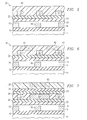
- Fig. 5 illustrates in cross section a small portion of a semiconductor wafer where the standard material layers noted above have been replaced with a single a layer of an organic polymer 40.
- the polymer layer 40 is deposited over the patterned metal layer 10 so as to planarize the surface and make it smooth and featureless.
- a sufficient thickness of the polymer 40 is deposited so that an upper portion of the polymer functions as a passivation layer to the metal layer 10. It is anticipated that a total thickness of the polymer layer 40 may be in the range of about 7 microns. It is realized that the thickness of the polymer layer 40 is a function of the thickness of the metal layer 10. Metal layers typically functioning as fringing capacitors are about 2 microns thick. Preferably, the thickness of the polymer 40 located above the metal pattern 10 is about 5 microns.
- the organic fluorocarbon family of polymers are not only well adapted for semiconductor processes, but such polymers are self planarizing. This means that no other processes are necessary to achieve a planarized top surface.
- the fluorocarbon polymer is spun or sprayed on the wafer surface, such material is initially in liquid form and thus sets with a smooth top surface. After a smooth surface is set into the organic material, the polymer is soft baked in the manner described above.
- the structure shown in Fig. 5 lends itself well to an efficient and low cost physical interface 30 that is thin, mechanically durable, compliant, and resistant to chemicals.
- the small distance between the top surface of the polymer 40 and the underlying capacitor metal network 10 provides low attenuation for the coupling of the electric field between the object and the fringing capacitor.
- the low attenuation of the electric field and the low dielectric constant exhibited by the fluorocarbon polymer make an excellent combination of properties for a high sensitivity capacitor sensor.
- the gettering agent 42 can be electrons or other ions suitable for immobilizing or pinning deleterious ions.
- Phosphorus can be implanted to getter sodium ions.
- the getter electrons or ions can be implanted into the surface of the polymer 40 by conventional ion implant equipment. The depth to which the electrons or ions are disposed under the surface of the polymer 40 is a function of the energy with which the electrons or ions are driven into the polymer 40.
- Electron implantation into polymers for use as microphones is disclosed in the publication entitled "A Micromachined Thin-film Teflon Electret Microphone", by Hsieh et. al., presented at Nepcon West, February 1999, Anaheim Ca. The disclosure of this publication is incorporated herein by reference.
- an implant mask such as a physical block or photoresist material
- the masking material can be deposited by conventional means on the surface of the wafer and patterned to open areas where the getter is to be implanted. In the masked areas of the wafer, the getter will not penetrate therethrough and thus will not be deposited in the underlying polymer 40.
- the selection of materials, the shape and configuration of the materials, and other parameters are important considerations.
- the principle of operation of the touch-sensitive chip is directly related to the nature of electric fields between the object and the sensor circuit which comprises the fringing capacitor network.
- the type of dielectric, thickness thereof and other physical properties determine the nature of the electric field.
- the dielectric differences between the ridges and valleys of the fingerprint produce corresponding variations in the electric fields, and thus influence the underlying fringing capacitor network.
- the strength or intensity of the electric field is sensed by the sensor capacitors and is converted to digital form for use in subsequent processing to reproduce the fingerprint pattern, or compare the same with one or more reference prints.
- the fluorocarbon polymer is well adapted for selective implant to modify or otherwise influence the characteristics of the electric field that exists between the object and the underlying circuit.
- Fig. 7 illustrates an embodiment of the invention where a fluorocarbon protective layer 50 has been deposited over the conventional silicon nitride layer 26 and silicon carbide layer 28. As noted above, this combination alone allows the two silicon-based layers 26 and 28 to be made thinner than in conventional practices.
- Implanted or otherwise deposited in the polymer layer 50 is an accumulation of particles 52, including electrons, ions or other matter that are capable of influencing an electric field.
- the particles 52 are implanted with an energy and dosage suitable to achieve a concentration that influences the electric field in the manner desired, it being realized that particles of various polarizations and concentrations will affect the electric field in different ways.
- Fig. 7 also illustrates that the particles 52 are selectively deposited in the polymer 50 so that the concentration of the particles 52 varies from one location to another.
- the concentration of the particles 52 is much higher in the location overlying the metal path 54, than in other regions in the polymer 50.
- the selective deposition of the particles can be achieved by forming a mask over the wafer, such as a photoresist type mask, and patterning the mask to open an area over the metal path 54. When the wafer is subjected to the implant operation, the particles will pass through the opening into the exposed polymer.
- the particles will not pass through the mask and thus the underlying polymer will not be implanted.
- Various other mask materials can be used for different types of particles and processes of deposition other than implant techniques. Indeed, various masking steps may be carried out in a sequence such that some areas can be implanted at different depths as compared to other areas, and/or implanted with different concentrations or types of particles.
- the electric field can be influenced in the manner desired.
- the electric field can be made to be more sensitive in some areas, and less sensitive in other areas. In those circuit areas where the electric field is to be minimized, then the overlying polymer area can be implanted with the type of particle that tends to cancel the electric field at that location.
- the electric field can, on the other hand, be made to accentuate the electric field in areas by embedding particles that achieve an enhancement of the electric field.
- the particles can also function to getter deleterious ions, as noted above.
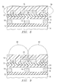
- Fig. 8 illustrates a semiconductor structure much like that shown in Fig. 5, with an electric field 56 that may be characteristic of such a structure. It is realized that the shape of the electric field 56 is only representative, it being realized that the actual shape would be much more complex. In any event, the electric field 56 that exists between the object and the capacitor sensor circuits is of a specified shape, and affects the sensor circuits accordingly.
- the electric field 60 is influenced such that the shape thereof is different from that shown in Fig. 8.
- the interaction of the respective electric fields themselves will produce an effective field that is different from the individual fields.
- Those skilled in the art can determine by experimentation the areas of the wafer and particle dosages and types that are necessary to achieve the desired influence on the electric fields.
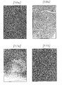
- the quality of the image, in terms of contrast, of a touch-sensitive chip is proportional to the amount of moisture on the skin of the person' s finger touching the physical interface. The higher the moisture content, the higher the image contrast between ridges and valleys.
- the image of a wet fingerprint is darker in contrast than a dry fingerprint. This is shown in Figs. 10a and 10b, where the person's finger in Fig. 10a is moist and in Fig. 10b the person's finger is dry. Excessive moisture and/or oils can interfere with the imaging of a fingerprint, in that such liquids can pool in the valleys between the ridges of the fingerprint and degrade the contrast between unique features of the fingerprint.
- Excessive moisture and/or oils on a person's finger can also leave a residue on the physical interface that contributes to ghosting during the imaging process. It can be seen that the moisture level of skin can thus be correlated with the level of contrast of the image. An algorithm can be developed that could thus measure the skin moisture content. It may also look at other areas of skin, other than the fingertip, to determine if there is more sensitivity on the palm, nose, or arm etc. It may then be useful to diagnose moisture levels for hand treatment. And, if sufficiently sensitive, the system could measure such things as dehydration levels for medical diagnosis, or diagnose other dermatological problems.
- the problem is that moisture from the finger directly overdrives the image, making it easier to leave a latent print.
- a "latent print” is a residual of the image after the finger is removed form the physical interface 30.
- the sensitivity of the latent fingerprint is a function of the material and surface states remaining on the interface surface of the sensor.
- touch-sensitive chips exhibit a hypersensitivity to residue, such as soap and hand lotion, that remains on the surface of the physical interface after the person's finger is removed therefrom.
- Sensors in general can become overly sensitive to residual moisture and oils. In extreme cases of hypersensitivity, the circuits are unable to capture a usable image.
- Fig. 11a illustrates the latency of a fingerprint on a physical interface constructed according to the prior art. Before any fingerprint was applied to the physical interface, the sensor circuits provided an image of a monotonic grey image. After a fingerprint was applied to the physical interface, and removed, the residual fingerprint that was effectively sensed was that shown in Fig. 11a.
- the substantial reduction in latency of fingerprints on the fluorocarbon polymer is related to its hydrophobic and oleophobic characteristics. It is known that the presence of polarized liquids, such as moisture, skin oils, hand lotion, etc., can fill the valleys between the ridges of fingerprint. Hydrophobic and oleophobic surfaces, such as the surface of a fluorocarbon polymer, ficilitate the dispersion of such liquids from the valleys and thereby reduce or eliminate the adverse latency effects. The surface of the fluorocarbon polymer aids in the removal of the moisture between the ridges of het fingerprint by way of capillary action. The problem of "wet finger" is thus reduced substantially.
- a fluorocarbon polymer can be employed with integrated circuits to provide a robust physical interface thereto.
- the polymer can be used in addition to conventional passivation layers, or in replacement thereof.
- the polymer can have particles embedded therein over the entire area, or in selected areas to provide a getter agent for deleterious ions, or to influence the electric field, or both.
Landscapes
- Engineering & Computer Science (AREA)
- Human Computer Interaction (AREA)
- Physics & Mathematics (AREA)
- General Physics & Mathematics (AREA)
- Multimedia (AREA)
- Theoretical Computer Science (AREA)
- Measurement Of Length, Angles, Or The Like Using Electric Or Magnetic Means (AREA)
- Formation Of Insulating Films (AREA)
- Structures Or Materials For Encapsulating Or Coating Semiconductor Devices Or Solid State Devices (AREA)
Applications Claiming Priority (2)
| Application Number | Priority Date | Filing Date | Title |
|---|---|---|---|
| US10996 | 2001-11-30 | ||
| US10/010,996 US6707093B2 (en) | 2001-11-30 | 2001-11-30 | Selective ionic implantation of fluoropolymer film to modify the sensitivity of underlying sensing capacitors |
Publications (2)
| Publication Number | Publication Date |
|---|---|
| EP1321981A2 true EP1321981A2 (de) | 2003-06-25 |
| EP1321981A3 EP1321981A3 (de) | 2006-10-11 |
Family
ID=21748400
Family Applications (1)
| Application Number | Title | Priority Date | Filing Date |
|---|---|---|---|
| EP02257811A Ceased EP1321981A3 (de) | 2001-11-30 | 2002-11-12 | Selektive Ionenimplantation in einer Filmstruktur aus Fluoropolymer zur Veränderung der Empfindlichkeit der darunter liegenden kapazitiven Sensoren |
Country Status (3)
| Country | Link |
|---|---|
| US (2) | US6707093B2 (de) |
| EP (1) | EP1321981A3 (de) |
| JP (1) | JP2003188319A (de) |
Cited By (1)
| Publication number | Priority date | Publication date | Assignee | Title |
|---|---|---|---|---|
| EP3304418A4 (de) * | 2015-06-08 | 2019-01-23 | Fingerprint Cards AB | Fingerabdruckerfassende vorrichtung mit heterogener beschichtungsstruktur mit einem klebstoff |
Families Citing this family (14)
| Publication number | Priority date | Publication date | Assignee | Title |
|---|---|---|---|---|
| CN100380596C (zh) | 2003-04-25 | 2008-04-09 | 株式会社半导体能源研究所 | 液滴排出装置、图案的形成方法及半导体装置的制造方法 |
| US7358741B2 (en) * | 2004-05-25 | 2008-04-15 | Alps Electric Co., Ltd | Electrostatic detection apparatus and method, and coordinate detection program |
| US8158517B2 (en) * | 2004-06-28 | 2012-04-17 | Semiconductor Energy Laboratory Co., Ltd. | Method for manufacturing wiring substrate, thin film transistor, display device and television device |
| US7424136B2 (en) * | 2005-10-18 | 2008-09-09 | Authentec, Inc. | Finger sensing with enhanced mounting and associated methods |
| US8358816B2 (en) * | 2005-10-18 | 2013-01-22 | Authentec, Inc. | Thinned finger sensor and associated methods |
| US8093698B2 (en) * | 2006-12-05 | 2012-01-10 | Spansion Llc | Gettering/stop layer for prevention of reduction of insulating oxide in metal-insulator-metal device |
| DE102007004844B4 (de) * | 2007-01-31 | 2011-05-05 | Infineon Technologies Ag | Verfahren zur Herstellung eines Bauteils und Bauteil |
| US9280239B2 (en) * | 2008-05-22 | 2016-03-08 | Plantronics, Inc. | Touch sensitive controls with weakly conductive touch surfaces |
| US20110279398A1 (en) * | 2010-05-12 | 2011-11-17 | Harald Philipp | Touch screen electrode enhancements |
| CN102968200B (zh) * | 2011-09-01 | 2016-08-03 | 宸美(厦门)光电有限公司 | 镜片触控装置及其制程方法 |
| TWI533232B (zh) * | 2014-12-11 | 2016-05-11 | 義隆電子股份有限公司 | 具靜電防護結構的指紋感測器 |
| MY191331A (en) | 2016-12-30 | 2022-06-16 | Intel Corp | Substrate with gradiated dielectric for reducing impedance mismatch |
| US11157717B2 (en) * | 2018-07-10 | 2021-10-26 | Next Biometrics Group Asa | Thermally conductive and protective coating for electronic device |
| US11817293B2 (en) * | 2020-01-10 | 2023-11-14 | The Research Foundation For The State University Of New York | Photoresist layers of semiconductor components including electric fields, system, and methods of forming same |
Family Cites Families (16)
| Publication number | Priority date | Publication date | Assignee | Title |
|---|---|---|---|---|
| US3639816A (en) * | 1970-08-10 | 1972-02-01 | Itt | Vacuum capacitor with solid dielectric |
| US4358677A (en) * | 1980-05-22 | 1982-11-09 | Siemens Corporation | Transducer for fingerprints and apparatus for analyzing fingerprints |
| US4977297A (en) | 1981-08-20 | 1990-12-11 | E. I. Du Pont De Nemours And Company | Amorphous copolymers of perfluoro-2,2-dimethyl-1,3-dioxole |
| US4982056A (en) | 1981-08-20 | 1991-01-01 | E. I. Du Pont De Nemours And Company | Amorphous copolymers of perfluoro-2,2-dimethyl-1,3-dioxide |
| US5198384A (en) * | 1991-05-15 | 1993-03-30 | Micron Technology, Inc. | Process for manufacturing a ferroelectric dynamic/non-volatile memory array using a disposable layer above storage-node junction |
| US6114862A (en) | 1996-02-14 | 2000-09-05 | Stmicroelectronics, Inc. | Capacitive distance sensor |
| FR2749955B1 (fr) | 1996-06-14 | 1998-09-11 | Thomson Csf | Systeme de lecture d'empreintes digitales |
| FR2755526B1 (fr) | 1996-11-05 | 1999-01-22 | Thomson Csf | Systeme de lecture d'empreintes digitales avec resistances de chauffage integrees |
| JP2910713B2 (ja) * | 1996-12-25 | 1999-06-23 | 日本電気株式会社 | 半導体装置の製造方法 |
| US6017829A (en) * | 1997-04-01 | 2000-01-25 | Micron Technology, Inc. | Implanted conductor and methods of making |
| US6088471A (en) * | 1997-05-16 | 2000-07-11 | Authentec, Inc. | Fingerprint sensor including an anisotropic dielectric coating and associated methods |
| US6091082A (en) * | 1998-02-17 | 2000-07-18 | Stmicroelectronics, Inc. | Electrostatic discharge protection for integrated circuit sensor passivation |
| US6060383A (en) * | 1998-08-10 | 2000-05-09 | Nogami; Takeshi | Method for making multilayered coaxial interconnect structure |
| JP2000133710A (ja) * | 1998-10-26 | 2000-05-12 | Tokyo Electron Ltd | 半導体装置及びその製造方法 |
| WO2001036905A1 (fr) * | 1999-11-18 | 2001-05-25 | Asahi Glass Company, Limited | Lecteur d'empreintes digitales |
| US20020164868A1 (en) * | 2001-05-02 | 2002-11-07 | Ting-Chang Chang | Method for forming a silicon dioxide-low k dielectric stack |
-
2001
- 2001-11-30 US US10/010,996 patent/US6707093B2/en not_active Expired - Lifetime
-
2002
- 2002-11-12 EP EP02257811A patent/EP1321981A3/de not_active Ceased
- 2002-11-29 JP JP2002347852A patent/JP2003188319A/ja active Pending
-
2003
- 2003-08-08 US US10/637,414 patent/US6759326B2/en not_active Expired - Lifetime
Cited By (1)
| Publication number | Priority date | Publication date | Assignee | Title |
|---|---|---|---|---|
| EP3304418A4 (de) * | 2015-06-08 | 2019-01-23 | Fingerprint Cards AB | Fingerabdruckerfassende vorrichtung mit heterogener beschichtungsstruktur mit einem klebstoff |
Also Published As
| Publication number | Publication date |
|---|---|
| JP2003188319A (ja) | 2003-07-04 |
| US6759326B2 (en) | 2004-07-06 |
| US6707093B2 (en) | 2004-03-16 |
| US20030104647A1 (en) | 2003-06-05 |
| EP1321981A3 (de) | 2006-10-11 |
| US20040038515A1 (en) | 2004-02-26 |
Similar Documents
| Publication | Publication Date | Title |
|---|---|---|
| US6762470B2 (en) | Fingerprint sensor having a portion of the fluorocarbon polymer physical interface layer amorphized | |
| EP1316994A2 (de) | Verwendung von Fluorpolymerbeschichtungen zur Planarisierung und Passivierung von integrierten Schaltungen | |
| US6707093B2 (en) | Selective ionic implantation of fluoropolymer film to modify the sensitivity of underlying sensing capacitors | |
| US6740945B2 (en) | Apparatus and method for contacting a conductive layer | |
| US6737329B2 (en) | Static charge dissipation pads for sensors | |
| US6686546B2 (en) | Static charge dissipation for an active circuit surface | |
| US6555888B2 (en) | Electrostatic discharge protection for sensors | |
| US6518083B2 (en) | Surface shape recognition sensor and method of manufacturing the same | |
| EP0789334B1 (de) | Integrierte Schaltungsanordnung mit einer den integrierten Schaltbaustein offenlegenden Öffnung und entsprechende Verfahren | |
| EP1017009B1 (de) | Vorrichtung und Verfahren zur Verbindung einer leitfähigen Sensorschicht | |
| KR20010012636A (ko) | 이방성 유전 코팅을 포함하는 지문 센서 및 그 제조방법 | |
| US6326227B1 (en) | Topographical electrostatic protection grid for sensors | |
| EP0985196A1 (de) | Fingerabdrucksensor mit verstärkungssteuerungsmerkmalen und dazugehörige verfahren | |
| US6091132A (en) | Passivation for integrated circuit sensors | |
| JP3516944B2 (ja) | 表面形状認識用センサおよびこの製造方法 |
Legal Events
| Date | Code | Title | Description |
|---|---|---|---|
| PUAI | Public reference made under article 153(3) epc to a published international application that has entered the european phase |
Free format text: ORIGINAL CODE: 0009012 |
|
| AK | Designated contracting states |
Designated state(s): AT BE BG CH CY CZ DE DK EE ES FI FR GB GR IE IT LI LU MC NL PT SE SK TR |
|
| AX | Request for extension of the european patent |
Extension state: AL LT LV MK RO SI |
|
| PUAL | Search report despatched |
Free format text: ORIGINAL CODE: 0009013 |
|
| RIC1 | Information provided on ipc code assigned before grant |
Ipc: G06K 9/20 20060101ALI20060831BHEP Ipc: G06K 9/00 20060101AFI20060831BHEP |
|
| AK | Designated contracting states |
Kind code of ref document: A3 Designated state(s): AT BE BG CH CY CZ DE DK EE ES FI FR GB GR IE IT LI LU MC NL PT SE SK TR |
|
| AX | Request for extension of the european patent |
Extension state: AL LT LV MK RO SI |
|
| 17P | Request for examination filed |
Effective date: 20070330 |
|
| AKX | Designation fees paid |
Designated state(s): DE FR GB IT |
|
| 17Q | First examination report despatched |
Effective date: 20071129 |
|
| 18R | Application refused |
Effective date: 20081212 |
|
| STAA | Information on the status of an ep patent application or granted ep patent |
Free format text: STATUS: THE APPLICATION HAS BEEN REFUSED |
|
| R18R | Application refused (corrected) |
Effective date: 20081119 |