EP1318425A2 - Catadioptric optical system and exposure apparatus equipped with the same - Google Patents
Catadioptric optical system and exposure apparatus equipped with the same Download PDFInfo
- Publication number
- EP1318425A2 EP1318425A2 EP03000101A EP03000101A EP1318425A2 EP 1318425 A2 EP1318425 A2 EP 1318425A2 EP 03000101 A EP03000101 A EP 03000101A EP 03000101 A EP03000101 A EP 03000101A EP 1318425 A2 EP1318425 A2 EP 1318425A2
- Authority
- EP
- European Patent Office
- Prior art keywords
- optical system
- catadioptric optical
- catadioptric
- mirrors
- plane
- Prior art date
- Legal status (The legal status is an assumption and is not a legal conclusion. Google has not performed a legal analysis and makes no representation as to the accuracy of the status listed.)
- Granted
Links
Images





Classifications
-
- G—PHYSICS
- G02—OPTICS
- G02B—OPTICAL ELEMENTS, SYSTEMS OR APPARATUS
- G02B17/00—Systems with reflecting surfaces, with or without refracting elements
- G02B17/08—Catadioptric systems
- G02B17/0804—Catadioptric systems using two curved mirrors
- G02B17/0812—Catadioptric systems using two curved mirrors off-axis or unobscured systems in which all of the mirrors share a common axis of rotational symmetry
-
- G—PHYSICS
- G02—OPTICS
- G02B—OPTICAL ELEMENTS, SYSTEMS OR APPARATUS
- G02B17/00—Systems with reflecting surfaces, with or without refracting elements
- G02B17/08—Catadioptric systems
- G02B17/0892—Catadioptric systems specially adapted for the UV
-
- G—PHYSICS
- G03—PHOTOGRAPHY; CINEMATOGRAPHY; ANALOGOUS TECHNIQUES USING WAVES OTHER THAN OPTICAL WAVES; ELECTROGRAPHY; HOLOGRAPHY
- G03F—PHOTOMECHANICAL PRODUCTION OF TEXTURED OR PATTERNED SURFACES, e.g. FOR PRINTING, FOR PROCESSING OF SEMICONDUCTOR DEVICES; MATERIALS THEREFOR; ORIGINALS THEREFOR; APPARATUS SPECIALLY ADAPTED THEREFOR
- G03F7/00—Photomechanical, e.g. photolithographic, production of textured or patterned surfaces, e.g. printing surfaces; Materials therefor, e.g. comprising photoresists; Apparatus specially adapted therefor
- G03F7/70—Microphotolithographic exposure; Apparatus therefor
- G03F7/70216—Mask projection systems
- G03F7/70225—Optical aspects of catadioptric systems, i.e. comprising reflective and refractive elements
-
- G—PHYSICS
- G03—PHOTOGRAPHY; CINEMATOGRAPHY; ANALOGOUS TECHNIQUES USING WAVES OTHER THAN OPTICAL WAVES; ELECTROGRAPHY; HOLOGRAPHY
- G03F—PHOTOMECHANICAL PRODUCTION OF TEXTURED OR PATTERNED SURFACES, e.g. FOR PRINTING, FOR PROCESSING OF SEMICONDUCTOR DEVICES; MATERIALS THEREFOR; ORIGINALS THEREFOR; APPARATUS SPECIALLY ADAPTED THEREFOR
- G03F7/00—Photomechanical, e.g. photolithographic, production of textured or patterned surfaces, e.g. printing surfaces; Materials therefor, e.g. comprising photoresists; Apparatus specially adapted therefor
- G03F7/70—Microphotolithographic exposure; Apparatus therefor
- G03F7/70216—Mask projection systems
- G03F7/70275—Multiple projection paths, e.g. array of projection systems, microlens projection systems or tandem projection systems
-
- G—PHYSICS
- G03—PHOTOGRAPHY; CINEMATOGRAPHY; ANALOGOUS TECHNIQUES USING WAVES OTHER THAN OPTICAL WAVES; ELECTROGRAPHY; HOLOGRAPHY
- G03F—PHOTOMECHANICAL PRODUCTION OF TEXTURED OR PATTERNED SURFACES, e.g. FOR PRINTING, FOR PROCESSING OF SEMICONDUCTOR DEVICES; MATERIALS THEREFOR; ORIGINALS THEREFOR; APPARATUS SPECIALLY ADAPTED THEREFOR
- G03F7/00—Photomechanical, e.g. photolithographic, production of textured or patterned surfaces, e.g. printing surfaces; Materials therefor, e.g. comprising photoresists; Apparatus specially adapted therefor
- G03F7/70—Microphotolithographic exposure; Apparatus therefor
- G03F7/70216—Mask projection systems
- G03F7/70358—Scanning exposure, i.e. relative movement of patterned beam and workpiece during imaging
Definitions
- the present invention relates to a catadloptric optical system and a projection exposure apparatus equipped with the catadioptric optical system suitable when manufacturing in a photolithography process, for example, a semiconductor device or a liquid crystal display device.
- the invention relates to a catadioptric optical system suitable for a scanning type projection exposure apparatus.
- a projection exposure apparatus by which a pattern image formed on a photomask or reticle (collectively referred to as "reticle” hereinafter) is projected and exposed onto a wafer, a glass plate, etc. coated with a photoresist or the like via a projection optical system.
- reticle a photomask or reticle
- NA numerical aperture
- the optical perrormance may be affected by, for example, light absorption in glass material and on an anti-reflection film on the lens surface.
- the oscillation bandwidth of laser light sources with an oscillation wavelength of 200 nm or less has been considerably narrowed, the bandwidth has still a certain wavelength width.
- correction of chromatic aberration of the order of pm (pico meter) is required.
- the optical system disclosed in the above-mentioned Japanese Unexamined Patent Publication Hei No. 5-173065 is a refraction type lens system made from a single kind of glass material, and its chromatic aberration is too large to be used with a light source having a wavelength width.
- a reflection type optical system utilizing power (refractive power) of a concave mirror and the like does not effect chromatic aberration and, with respect to Petzval sum, creates a contribution with an opposite sign to a lens element.
- a so-called catadioptric optical system hereinafter referred to as "catadioptric optical system"
- a catadioptric optical system which. combines a catoptric optical system and a dioptric optical system together, can correct chromatic aberration as well as other various aberrations to a level of almost no aberration without increasing the number of lenses.
- a catadioptric optical system is an optical system having at least one lens element and at least one reflecting mirror with refractive power.
- optical elements constituting a optical system can all be disposed along a single optical axis.
- the optical system can be manufactured with high accuracy following an optical element adjustment method conventionally used in the projection optical system manufacture.
- the system requires a central light-shielding portion to shield light beam propagating along the optical axis, resulting in the contrast deterioration of a pattern of a certain frequency.
- the present invention has been made in view of the above problems, and the object of the invention is to provide a catadioptric optical system in which chromatic aberration is well corrected in the extreme ultraviolet wavelength region, in particular, even in the wavelength region of 200 nm or less, and a NA (0.6 or more) necessary for high resolution is secured, and the number of refractive and reflecting components is reduced as much as possible; a projection exposure apparatus equipped with the optical system.
- the present invention provides a catadioptric optical system, which comprises a first catadioptric type imaging optical system for forming an intermediate image of a first surface and a second refraction type imaging optical system for telecentically forming the final image of said first surface onto a second surface based on said light from said intermediate image; wherein said first imaging optical system has a lens group including at least one positive lens element, a first reflecting surface which reflects light passed through said lens group, and a second reflecting surface for directing light reflected by said first reflecting surface to said second imaging optical system; at least one of said first and second reflecting surfaces is a concave reflecting surface; and said second imaging optical system has an aperture diaphragm; wherein all of the optical elements of said catadioptric optical system are disposed on a single linear optical axis, and said first surface and said second surface are plane surfaces which are approximately mutually parallel; and wherein an exit pupil of said catadioptric optical system is approximately circular.
- the second reflecting surface has an aperture portion (hole) at an off-axis position for making light from the first surface pass or pass through in the direction of the first reflecting surface
- the first reflecting surface also has an aperture portion (hole) for making the light reflected by said second reflecting surface pass or pass through in the direction of the second imaging optical system.
- That the exit pupil is substantially circular means that there is no shielding object in the neighborhood of the center of the optical axis.
- the following condition is preferably satisfied: 0.04 ⁇
- the following condition is preferably satisfied: 0.6 ⁇
- the following condition is preferably satisfied: 0.3 ⁇
- a projection exposure apparatus comprising:
- the system is a catadioptric optical system provided with a first catadioptric type imaging optical system G1 for forming an intermediate image I1 of a first surface 3 and with a second refraction type imaging optical system G2 for telecentrically forming the final image of the first surface 3 onto a second surface 9 (wafer surface, i.e., the final image plane) based on light from the intermediate image.
- a first catadioptric type imaging optical system G1 for forming an intermediate image I1 of a first surface 3
- a second refraction type imaging optical system G2 for telecentrically forming the final image of the first surface 3 onto a second surface 9 (wafer surface, i.e., the final image plane) based on light from the intermediate image.
- the first optical system G1 has a lens group including at least one positive lens element, a first reflecting surface M1 which reflects light passed through the lens group and is substantially collimated, and a second reflecting surface M2 for directing light reflected by the first reflecting surface M1 to the second imaging optical system G2; and at least one of the first and second reflecting surfaces is a concave reflecting surface.
- the second imaging optical system G2 has aperture diaphragm AS, all of the optical elements of the catadioptric optical system are disposed on a single linear optical axis AX, the first surface 3 and the second surface 9 are plane surfaces which are substantially mutually parallel; and an exit pupil of the catadioptric optical system is substantially circular.
- a structurally reasonable catadioptric optical system is achieved by making the effective projected area an annular shape and by preventing mutual interference of optical elements through appropriately positioning the first and second reflecting surfaces M1 end M2.
- the following condition is preferably satisfied: (1) 0.04 ⁇
- the condition (1) defines an appropriate power range of the concave reflecting surface.
- positive Petzval sum created by refractive lenses is corrected by negative Petzval sum created by the concave mirror.
- the power is over the upper limit value of the condition (1), the positive Petzval sum created by refractive lenses cannot be sufficiently corrected, and the flatness of the image deteriorates.
- the power is below the lower limit value of the condition (1), the Petzval sum is overcorrected, and the flatness of the image deteriorates similarly
- the following condition is preferably satisfied: (2) 0.6 ⁇
- the condition (2) defines an appropriate magnification range of the concave reflecting mirror. When the magnification is over the upper limit value of the condition (2) or is below the lower limit value of the condition (2), symmetricity of the first imaging system G1 is seriously affected, large coma aberration being produced, and causes the image deterioration.
- the following condition is preferably satisfied: (3) 0.3 ⁇
- the condition (3) defines an appropriate magnification range of the first imaging optical system G1. When the magnification is over the upper limit value of the condition (3) or is below the lower limit value of the condition (3), power balance collapses, causing distortion aberration (distortion) and coma aberration, and the imaging performance deteriorates.
- the first imaging optical system G1 has a light beam which intersects at least three times a plane P1 perpendicular to the optical axis AX.
- the effective projected area an annular shape, the light and the optical elements such as the reflecting surfaces M1 and M2 can be positioned so as not to physically interfere with each other.
- the catadioptric optical system of the present invention is telecentric on the second surface 9 side (wafer surface side), but it is preferable that the optical system be additionally telecentric on the first surface 3 side (reticle surface side).
- FIG. 1 is a drawing schematically illustrating the overall configuration of a projection exposure apparatus equipped with a projection optical system in accordance with any embodiment of the present invention optical systems.
- a Z-axis is set parallel to the optical axis AX of the projection optical system 8 constituting the projection exposure optical system
- an X-axis is set parallel to the plane of the drawing of FIG.1
- a Y-axis is set perpendicular to the plane of the drawing, both of X- and Y- axes being in a plane perpendicular to the optical axis AX.
- a reticle 3, as a projection original plate, on which a predetermined circuit pattern is formed is disposed on the object plane of the projection optical system 8, and a wafer 9, as a substrate, coated with a photoresist is disposed on the image plane of the projection optical system 8.
- One or more folding mirrors for changing the optical path direction are disposed, as required, on the optical path from the light source 1 to the illumination optical system 2.
- the illumination optical system 2 comprises optical systems such as an optical integrator constituted of, for example, a flyeye lens or an internal reflection type integrator for forming a plane light source having a predetermined size and shape; a variable field stop (reticle blind) for defining the size and shape of an illumination area on the reticle 3; and a field stop imaging optical system for projecting the image of this field stop on the reticle.
- optical systems such as an optical integrator constituted of, for example, a flyeye lens or an internal reflection type integrator for forming a plane light source having a predetermined size and shape; a variable field stop (reticle blind) for defining the size and shape of an illumination area on the reticle 3; and a field stop imaging optical system for projecting the image of this field stop on the reticle.
- an optical system from the light source 1 to the field stop the illumination optical system disclosed in U.S. Patent No. 5,345,292 may be applied.
- the reticle 3 is, via reticle holder 4, held on reticle stage 5 parallel to the XY plane. On the reticle 3 is formed a pattern to be transferred, and the overall pattern area is illuminated with light from the illumination optical system 2.
- the reticle stage 5 is so configured that the stage is two-dimensionally movable along a reticle plane (i.e., the XY plane) by the effect of a drive system, not shown, and that the coordinate position of the stage is measured by interferometer 7 using reticle moving mirror 6 and is position-controlled.
- the projection optical system 8 has a variable aperture diaphragm AS (see FIG. 2) near its pupil and is substantially telecentric on both of the reticle 3 and wafer 9 sides.
- the wafer 9 is, via a wafer holder 10, held on a wafer stage 11 parallel to the XY plane. Onto a substantially similar exposure area to the illuminated area on the reticle 3 is thus formed the pattern image.
- the wafer stage 11 is so configured that the stage is two-dimensionally movable along a wafer plane (i.e., the XY plane) by the effect of a drive system, not shown, and that the coordinate position of the stage is measured by interferometer 13 using wafer moving mirror 12 and thus the wafer stage is position-controlled.
- a wafer plane i.e., the XY plane
- the field view area on the mask 3 (illumination area) and the projection area (exposure area) on the wafer 9 both defined by the projection optical system 8 are rectangle-shaped areas having a short-side along the X-axis. Aligning the mask 3 and the wafer 9 is thus performed by using the drive systems and the interferometers (7, 13), and the wafer 9 is positioned onto the image plane of the projection optical system by the use of an autofocus/autoleveling system, not shown.
- the mask pattern is scanningly exposed onto an area on the wafer 9 of which width is equal to the long-side length of the exposure area and of which length is equal to the scanning (moving) length of the wafer 9.
- an inert gas atmosphere such as nitrogen or helium gas into which the exposure light is little absorbed.
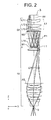
- FIG. 2 is a drawing illustrating a lens configuration of a catadioptric optical system in accordance with a first embodiment of the present invention.
- the system is a catadioptric optical system comprising a first catadioptric type imaging optical system G1 for forming an intermediate image I1 of a reticle (first surface) 3 and a second refraction type imaging optical system G2 for telecentrically forming the final image of the reticle surface 3 onto a wafer (second surface) 9 based on light from the intermediate image I1.
- the first imaging optical system G1 has a lens group L1 including at least one positive lens element, a first reflecting surface M1 which reflects light passed through the lens group L1, and a second reflecting surface M2 for directing light reflected by the first reflecting surface M1 to the second imaging optical system G2, at least one of the first and second reflecting surfaces being a concave reflecting surface, and the second imaging optical system G2 having an aperture diaphragm AS. Further. all of the optical elements of the catadioptric optical system are disposed on a single linear optical axis AX, the reticle surface 3 and the wafer surface 9 are plane surfaces which are substantially mutually parallel; and an exit pupil of the catadioptric optical system is substantially circular.
- Table 1 values of items of the projection optical system in accordance with the first embodiment.
- numerals in the leftmost column represent the order of lens surfaces from the reticle 3 (first object plane) side
- r is the radius of curvature of the lens surface
- d is the lens surface interval from the lens surface to the next lens surface
- ⁇ is the overall magnification of the catadioptric optical system
- NA is the numerical aperture on the wafer side (the second surface side)
- ⁇ is the standard wavelength. Note that the refractive indexes of the glass used in the first embodiment equal to those in the second embodiment.
- ASP in the lens data represents an aspherical surface.
- y is the height in the direction normal to the optical axis
- Z is a displacement amount (sag amount) from the tangential plane at the apex of the aspherical surface to a position of the aspherical surface at the height y measured along the direction of the optical axis
- r is the radius of curvature at the apex
- ⁇ is a conical coefficient
- A-F are aspherical coefficients of the n-th order.
- FIG. 3 shows transverse aberrations (coma aberrations) of the catadioptric optical system in accordance with the embodiment in the meridional (tangential) and sagittal directions.
- Y indicates the image height
- aberrations are well-balancedly corrected in the overall exposure area in the catadioptric optical system of this embodiment in spite of the both-sides telecentricity along with the imaging performance deterioration due to the light absorption by the applied glass materials being prevented.
- FIG. 4 is a drawing illustrating a lens configuration of a catadioptric optical system in accordance with a second embodiment.
- the system is a catadioptric optical system comprising a first. catadioptric type imaging optical system G1 for forming an intermediate image I1 of a reticle (first surface) 3 and a second refraction type imaging optical system G2 for telecentrically forming the final image of the reticle surface 3 onto a wafer (second surface) 9 based on light from the intermediate image I1.
- the first imaging optical system G1 has a lens group L1 including at least one positive lens element, a first reflecting surface M1 which reflects light passed through the lens group L1, and a second reflecting surface M2 for directing light reflected by the first reflecting surface M1 to the second imaging optical system G2; at least one of the first and second reflecting surfaces is a concave reflecting surface; and the second imaging optical system G2 has an aperture diaphragm AS. Further, all of the optical elements of the catadioptric optical system are disposed on a single linear optical axis AX, the reticle surface 3 and the wafer surface 9 are plane surfaces which are substantially mutually parallel; and an exit pupil of the catadioptric optical system is substantially circular.
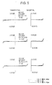
- FIG. 5 shows transverse aberration diagrams of the catadioptric optical system in accordance with the second embodiment. As can be clearly seen also from the aberration diagrams, aberrations are well-balancedly corrected in the overall exposure area.
- FIG. 6 is a drawing illustrating a lens configuration of a catadioptric optical system in accordance with a third embodiment.
- the system is a catadioptric optical system comprising a first catadioptric type imaging optical system G1 for forming an intermediate image I1 of a reticle (first surface) 3 and a second refraction type imaging optical system G2 for telecentrically forming the final image of the reticle surface 3 onto a wafer (second surface) 9 based on light from the intermediate image I1.
- the first imaging optical system G1 has a lens group L1 including at least one positive lens element, a first reflecting surface M1 which reflects light passed through the lens group L1, and a second reflecting surface M2 for directing light reflected by the first reflecting surface M1 to the second imaging optical system G2; at least one of the first and second reflecting surfaces is a concave reflecting surface; and the second imaging optical system G2 has an aperture diaphragm AS. Further, all of the optical elements of the catadioptric optical system are disposed on a single linear optical axis AX, the reticle surface 3 and the wafer surface 9 are plane surfaces which are substantially mutually parallel; and an exit pupil of the catadioptric optical system is substantially circular.
- Table 3 values of items of the projection optical system in accordance with the third embodiment. Note that reference codes in Table 3 are similarly defined as those in FIG. 1, aspherical surface ASP can be expressed by the above-described mathematical formula.
- FIG. 6 shows transverse aberration diagrams of the catadioptric optical system in accordance with the third embodiment.
- Y indicates the image height
- the above-mentioned embodiments are applied to a scanning type projection exposure apparatus using a step-and-scan method (scanning method) in which a mask and a wafer are synchronously scanned with the speed ratio equal to the exposure magnification ⁇ while each shot area on a wafer is exposed using an exposure area of circular arc shape (a shape partially cut out of an annular shape).
- scanning method scanning method
- a mask and a wafer are synchronously scanned with the speed ratio equal to the exposure magnification ⁇ while each shot area on a wafer is exposed using an exposure area of circular arc shape (a shape partially cut out of an annular shape).
- the above-mentioned embodiments can be applied also to a step-and-repeat type (one-shot type) projection exposure apparatus in which, after the mask pattern image being transferred onto one shot area on a wafer at one shot, a process wherein the mask pattern image is exposed onto a next shot area by two-dimensionally moving the wafer repetitively is repeated.
- a step-and-repeat type one-shot type
- a slit-like exposure area (a shape extending in a predetermined direction, for example, a long rectangle, a trapezoid, a long hexagon, a circular arc, etc.)
- a larger shot area on a wafer can be exposed without large-sizing the projection optical system.
- the invention is applied to a projection exposure apparatus used for the manufacture of semiconductor devices.
- the invention can be applied to, for example, an exposure apparatus transferring a display pattern onto a glass plate used for the manufacture of display devices including liquid crystal display devices, to an exposure apparatus transferring a display pattern onto a ceramics wafer used for the manufacture of thin film magnetic heads, to an exposure apparatus used for the manufacture of image pick-up devices (CCD, etc.).
- the invention can be applied to an exposure apparatus transferring a circuit pattern onto a glass substrate or a silicon wafer used for the manufacture of a reticle or a mask.
- present invention can be configured as the following (A) or (B) configuration.
- the present invention can provide a catadioptric optical system in which chromatic aberration is well corrected in the extreme ultraviolet wavelength region, in particular, even in the wavelength region of 200 nm or less, and a NA (0.6 or more) necessary for high resolution is secured, and the number of refractive and reflecting components is reduced as much as possible. Further, exposure light can be effectively used since light absorption is little because of the small number of reflecting elements and the like. Still further, the projection exposure apparatus of the present Invention, being equipped with the above-mentioned catadioptric optical system, has an advantage that fine mask patterns can be accurately transferred.
Landscapes
- Physics & Mathematics (AREA)
- General Physics & Mathematics (AREA)
- Optics & Photonics (AREA)
- Lenses (AREA)
- Exposure And Positioning Against Photoresist Photosensitive Materials (AREA)
- Exposure Of Semiconductors, Excluding Electron Or Ion Beam Exposure (AREA)
Abstract
Description
Further, the mirror is easily affected by vibration.
wherein said first imaging optical system has a lens group including at least one positive lens element, a first reflecting surface which reflects light passed through said lens group, and a second reflecting surface for directing light reflected by said first reflecting surface to said second imaging optical system; at least one of said first and second reflecting surfaces is a concave reflecting surface; and said second imaging optical system has an aperture diaphragm;
wherein all of the optical elements of said catadioptric optical system are disposed on a single linear optical axis, and said first surface and said second surface are plane surfaces which are approximately mutually parallel; and
wherein an exit pupil of said catadioptric optical system is approximately circular. Here, the second reflecting surface has an aperture portion (hole) at an off-axis position for making light from the first surface pass or pass through in the direction of the first reflecting surface, and the first reflecting surface also has an aperture portion (hole) for making the light reflected by said second reflecting surface pass or pass through in the direction of the second imaging optical system.
| | β | = 1/4 | |||
| NA=0.7 5 | |||
| λ = 193. 3nm | |||
| No. | r | d | Glass Material |
| 1: | -211.97583 | 30.000000 | SiO2 |
| 2: | -354.80161 | 35.347349 | |
| 3: | -8888.21083 | 38.000000 | SiO2 |
| 4: | -227.79960 | 0.944905 | |
| 5: | 303.84978 | 27.415767 | SiO2 |
| ASP: | |||
| κ=0.000000 | |||
| A=+0.743561×10⁻⁸ B=-0.230589×10⁻¹² | |||
| C=-0.115168×10⁻¹⁷ D=-0.753145×10⁻²² | |||
| 6: | 237634.15996 | 30.000000 | |
| 7: | ∞ (Plane) | 214.776416 | |
| 8: | -348.87932 | 12.000000 | SiO2 |
| 9: | 4267.07121 | 5.579827 | |
| 10: | -362.24910 | -5.579827 | (Reflecting surface) |
| ASP: | |||
| κ=3.260270 | |||
| A=+0.859110×10⁻⁸ B=+0.351935×10⁻¹² | |||
| C=-0.100064×10⁻¹⁵ D=+0.318170×10⁻¹⁹ | |||
| E=-0.489883×10⁻²³ | |||
| 11: | 4267.07087 | -12.000000 | SiO2 |
| 12: | -348.87932 | -214.776416 | |
| 13: | 642.80918 | 246.776416 | (Reflecting surface) |
| ASP: | |||
| κ=1.840470 | |||
| A=0.198825×10⁻⁸ B=0.556479×10⁻¹³ | |||
| C=0.597091×10⁻¹⁸ D=0.492729×10⁻²² | |||
| E=-0.103460×10⁻²⁶ | |||
| 14: | 208.71115 | 33.000000 | SiO2 |
| 15: | -2529.7293.0 | 257.546203 | |
| 16: | -1810.41832 | 14.500000 | SiO2 |
| ASP: | |||
| κ=0.000000 | |||
| A=-0.885983×10⁻⁷ B=-0.200044×10⁻¹¹ | |||
| C=-0.570861×10⁻¹⁶ D=+0.456578×10⁻²² | |||
| E=-0.493085×10⁻²⁵ | |||
| 17: | 851.98207 | 220.408225 | |
| 18: | 15200.59096 | 30.000000 | SiO2 |
| 19: | -268.76515 | 0.200000 | |
| 20: | 434.96005 | 36.013163 | CaF2 |
| ASP: | |||
| κ=0.000000 | |||
| A=-0.161380×10⁻⁷ B=+0.153066×10⁻¹² | |||
| C=+0.108604×10⁻¹⁷ D=+0.319975×10⁻²¹ | |||
| E=-0.101080×10⁻²⁵ | |||
| 21: | -345.83883 | 10.489902 | |
| 22: | -215.91874 | 20.000000 | SiO2 |
| 23: | -619.95152 | 0.200000 | |
| 24: | 415.08345 | 40.000000 | SiO2 |
| 25: | -1275.90912 | 26.288090 | |
| 26: | 324.91386 | 35.000000 | SiO2 |
| 27: | -740.00769 | 5.214992 | |
| ASP: | |||
| κ=0.000000 | |||
| A=+0.138330×10⁻⁷ B=+0.194125×10⁻¹² | |||
| C=-0.258860×10⁻¹³ D=-0.196062×10⁻²² | |||
| E=+0.363539×10⁻²⁶ | |||
| 28: | 140.91060 | 34.000000 | SiO2 |
| 29: | 1406.88948 | 0.500000 | |
| 30: | 355.40083 | 17.506069 | SiO2 |
| 31: | 98.27403 | 1.561573 | |
| 32: | 105.27944 | 75.940555 | SiO2 |
| 33: | 1597.37798 | 12.920542 |
SiO2 1.56032536 1.5603261 1.56032685
CaF2 1.50145434 1.5014548 1.50145526
| | β | = 1/6 | |||
| NA = 0. 75 | |||
| λ = 193. 3 nm | |||
| No. | r | d | Glass Material |
| 1: | 521.54601 | 23.000000 | SiO2 |
| 2: | -191794.5079 | 0.944905 | |
| 3: | 194.28987 | 30.000000 | SiO2 |
| ASP: | |||
| κ=0.000000 | |||
| A=-0.155326×10⁻⁸ B=-0.140791×10⁻¹² | |||
| C=+0.176234×10⁻¹⁷ D=-0.155625×10⁻²¹ | |||
| 4: | 452.66236 | 300.000000 | |
| 5: | -589.38426 | 12.000000 | SiO2 |
| 6: | 1106.79674 | 5.000000 | |
| 7: | -482.64964 | -5.000000 | (Reflecting surface) |
| ASP: | |||
| κ=7.430564 | |||
| A=+0.199000×10⁻⁸ B=-0.957889×10⁻¹² | |||
| C=-0.122172×10⁻¹⁵ D=+0.305937×10⁻¹⁹ | |||
| E=-0.126279×10⁻²² | |||
| 8: | 1106.79671 | -12.000000 | SiO2 |
| 9: | -589.38426 | -273.707398 | |
| 10: | 455.39924 | 477.535323 | (Reflecting surface) |
| ASP: | |||
| κ=0.000000 | |||
| A=+0.434199×10⁻⁹ B=+0.327908×10⁻¹⁴ | |||
| C=+0.360429×10⁻¹⁹ D=-0.622589×10⁻²⁴ | |||
| > 11: | 300.69546 | 29.000000 | SiO2 |
| 12: | -3836.44237 | 191.527911 | |
| 13: | -4996.75666 | 15.000000 | SiO2 |
| ASP: | |||
| κ=0.000000 | |||
| A=-0.601871E-07 B=-0.111865×10⁻¹¹ | |||
| C=-0.177478×10⁻¹⁶ D=+0.104425×10⁻²³ | |||
| E=-0.236872×10⁻²⁵ | |||
| 14: | 1631.22452 | 164.229823 | |
| 15: | 761.43970 | 32.000000 | SiO2 |
| 16: | -416.24467 | 7.787594 | |
| 17: | 385.90210 | 43.198650 | CaF2 |
| ASP: | |||
| κ=0.000000 | |||
| A=-0.127289×10⁻⁷ B=+0.112712×10⁻¹² | |||
| C=-0.237720×10⁻¹⁸ D=+0.283035×10⁻²¹ | |||
| E=-0.177785×10⁻²⁵ | |||
| 18: | -325.55463 | 16.575364 | |
| 19: | -220.30976 | 20.000000 | SiO2 |
| 20: | -755.61144 | 9.063759 | |
| 21: | 359.10784 | 37.871908 | SiO2 |
| 22: | -1575.91947 | 1.464560 | |
| 23: | 235.63612 | 32.000000 | SiO2 |
| 24: | -2200.62013 | 1.000000 | |
| ASP: | |||
| κ=0.000000 | |||
| A=+0.198616×10⁻⁷ B=-0.109623×10⁻¹² | |||
| C=0.106669×10⁻¹⁶ D=-0.466071×10⁻²¹ | |||
| E=+0.853932×10⁻²⁶ | |||
| 25: | 159.89570 | 33.600000 | SiO2 |
| 26: | 2158.79385 | 0.000000 | |
| 27: | 406.09986 | 9.500000 | SiO2 |
| 28: | 68.76384 | 4.196119 | |
| 29: | 70.58705 | 75.473363 | SiO2 |
| 30: | 2340.17874 | 9.379567 |
| | β | = 1/4 | |||
| NA=0.75 | |||
| λ = 157. 6 nm | |||
| No. | r | d | Glass Material |
| 1: | 314.69351 | 28.000000 | CaF2 |
| 2: | -934.65900 | 37.000000 | |
| ASP: | |||
| κ=0.000000 | |||
| A=-0.229218×10⁻⁷ B=÷0.947150×10⁻¹² | |||
| C=-0.128922×10⁻¹⁶ D=-0.190103×10⁻²⁰ | |||
| E=-0.386976×10⁻²⁵ | |||
| 3: | -639.17871 | 23.000000 | CaF2 |
| ASP: | |||
| κ =0.000000 | |||
| A=-0.108326×10⁻⁷ B=+0.924937×10⁻¹² | |||
| C=-0.326453×10⁻¹⁶ D=-0.342966×10⁻²⁰ | |||
| E=+0.132323×10⁻²⁵ | |||
| 4: | -318.93314 | 245.763430 | |
| 5: | -108.60441 | 10.000000 | CaF2 |
| ASP: | |||
| κ=0.495309 | |||
| A=0.486675×10⁻⁷ B=0.492347×10⁻¹¹ | |||
| C=-0.606490×10⁻¹⁶ D=0.180500×10⁻¹⁸ | |||
| E=-0.766603×10⁻²³ F=0.138880×10⁻²⁶ | |||
| 6: | -2160.76276 | 14.249561 | |
| 7: | -165.34978 | -14.249561 | (Reflecting surface) |
| ASP: | |||
| κ=1.132286 | |||
| A=+0.201000×10⁻⁷ B=+0.102160×10⁻¹¹ | |||
| C=-0.209696×10⁻¹⁶ D=+0.126536×10⁻¹⁹ | |||
| E=+0.429651×10⁻²⁴ F=-0.160033×10⁻²⁹ | |||
| 8: | -2160.76276 | -10.000000 | CaF2 |
| 9: | -108.60441 | -245.763430 | |
| ASP: | |||
| κ=0.495309 | |||
| A=+0.486675×10⁻⁷ B=+0.492347×10⁻¹¹ | |||
| C=-0.606490×10⁻¹⁶ D=+0.180500×10⁻¹⁸ | |||
| E=-0.766603×10⁻²³ F=+0.138880×10⁻²⁶ | |||
| 10: | -318.93314 | -23.000000 | CaF2 |
| 11: | -639.17869 | -4.391997 | |
| ASP: | |||
| κ=0.000000 | |||
| A=-0.108326×10⁻⁷ B=+0.924936×10⁻¹² | |||
| C=-0.326453×10⁻¹⁶ D=-0.342966×10⁻²⁰ | |||
| E=+0.132323×10⁻²⁵ | |||
| 12: | -1183.44883 | 4.391997 (Reflecting surface) | |
| ASP: | |||
| κ=0.000000 | |||
| A=-0.183262×10⁻¹⁰ B=-0.246349×10⁻¹² | |||
| C=+0.147599×10⁻¹⁶ D=+0.182045×10⁻²⁰ | |||
| E=-0.115790×10⁻²⁵ | |||
| 13: | -639.17869 | 23.000000 | CaF2 |
| ASP: | |||
| κ=0.000000 | |||
| A=-0.108326×10⁻⁷ B=+0.924936×10⁻¹² | |||
| C=-0.326453×10⁻¹⁶ D=-0.342966×10⁻²⁰ | |||
| E=+0.132323×10⁻²⁵ | |||
| 14: | -318.93314 | 300.763420 | |
| 15: | 756.86009 | 41.000000 | CaF2 |
| 16: | -412.30872 | 15.942705 | |
| ASP : | |||
| κ=0.000000 | |||
| A=+0.361860×10⁻⁸ B=+0.893121×10⁻¹⁴ | |||
| C=+0.135118×10⁻¹⁸ D=-0.735265×10⁻²³ | |||
| E=+0.151108×10⁻²⁷ | |||
| 17: | 382.45831 | 36.000000 | CaF2 |
| 18: | 2411.92028 | 120.195566 | |
| 19: | 203.57233 | 23.670903 | CaF2 |
| ASP: | |||
| κ=0,000000 | |||
| A=-0.666118×10⁻⁸ B=-0.225767×10⁻¹² | |||
| C=-0.790187×10⁻¹⁹ D=-0.460596×10⁻²¹ | |||
| E=0.210563×10⁻²⁵ F=-0.570908×10⁻³⁰ | |||
| 20: | 174.15615 | 417.834922 | |
| 21: | 164.52297 | 20.000000 | CaF2 |
| ASP: | |||
| κ=0.000000 | |||
| A=+0.153241×10⁻⁷ B=+0.610531×10⁻¹² | |||
| C=+0.252256×10⁻¹⁵ D=-0.150451×10⁻²⁰ | |||
| E=+0.326670×10⁻²³ F=-0.132886×10⁻²⁷ | |||
| 22: | 746.82563 | 20.284156 | |
| 23: | 93.58470 | 23.000000 | CaF2 |
| ASP: | |||
| κ=0.000000 | |||
| A=-0.267761×10⁻⁷ B=+0.970828×10⁻¹² | |||
| C=+0.117557×10⁻¹⁵ D=+0.718106×10⁻¹⁹ | |||
| E=-0.162733×10⁻²² F=+0.586684×10⁻²⁶ | |||
| 24: | 256.99945 | 21.338588 | |
| 25: | -129.21983 | 16.000000 | CaF2 |
| ASP: | |||
| κ=0.000000 | |||
| A=-0.588690×10⁻⁸ B=0.461959×10⁻¹² | |||
| C=0.130813×10⁻¹⁴ D=-0.849445×10⁻¹⁹ | |||
| E=-0.123125×10⁻²² F=+0.290566×10⁻²⁶ | |||
| 26: | -219.48522 | 1.000000 | |
| 27: | 102.75126 | 19.500000 | CaF2 |
| ASP: | |||
| κ=0.000000 | |||
| A=-0.862905×10⁻⁷ B=-0.119006×10⁻¹⁰ | |||
| C=-0.124879×10⁻¹⁴ D=-0.367913×10⁻¹⁸ | |||
| E=-0.451018×10⁻²² F=+0.119726×10⁻²⁶ | |||
| 28: | 593.36680 | 1.000000 | |
| 29: | 83.17946 | 18.815833 | CaF2 |
| ASP: | |||
| κ=0.111409 | |||
| A=-0.393239×10⁻⁷ B=-0.723984×10⁻¹¹ | |||
| C=-0.679503×10⁻¹⁴ D=-0.115217×10⁻¹⁷ | |||
| E=-0.763652×10⁻²² F=+0.381047×10⁻²⁵ | |||
| 30: | 197.09247 | 1.000000 | |
| 31: | 110.23581 | 43.599536 | CaF2 |
| ASP: | |||
| κ=0.000000 | |||
| A=+0.850436×10⁻⁹ B=+0.126341×10⁻¹⁰ | |||
| C=+0.168625×10⁻¹³ D=+0.782396×10⁻¹⁷ | |||
| E=-0.233726×10⁻²⁰ F=+0.333624×10⁻²⁴ | |||
| 32: | ∞ (Plane) | 9.100000 |
λ=157.6nm+1.29pm 157.6nm 157.6nm-1.29pm
CaF2 1.55999383 1.56 1.56000617
However, in addition to a projection exposure apparatus used for manufacture of semiconductor devices, the invention can be applied to, for example, an exposure apparatus transferring a display pattern onto a glass plate used for the manufacture of display devices including liquid crystal display devices, to an exposure apparatus transferring a display pattern onto a ceramics wafer used for the manufacture of thin film magnetic heads, to an exposure apparatus used for the manufacture of image pick-up devices (CCD, etc.). Also, the invention can be applied to an exposure apparatus transferring a circuit pattern onto a glass substrate or a silicon wafer used for the manufacture of a reticle or a mask.
Claims (29)
- A catadioptric optical system for forming an intermediate image of a first surface within the catadioptric optical system and for forming a final image of the first surface onto a second surface, comprising:wherein at least two mirrors of the plurality of mirrors are arranged in an optical path between the first surface and the intermediate image, andan optical axis:an aperture stop which is arranged in an optical path between the intermediate image and the second surface;a plurality of mirrors which are arranged on the optical axis; anda plurality of lens elements which are arranged on the optical axis;
wherein at least one lens element of the plurality of lens elements are arranged in an optical path between the aperture stop and the second surface. - A catadioptric optical system according to claim 1, wherein the at least one lens element of the plurality of lens elements is arranged in an optical path between the first surface and the at least two mirrors.
- A catadioptric optical system according to claim 2, wherein the lens element arranged in the optical path between the first surface and the at least two mirrors has a positive refractive power.
- A catadioptric optical system according to any one of claims 1-3, wherein the at least two mirrors include at least one concave mirror.
- A catadioptric optical system according to any one of claims 1-4, wherein the first surface and the second surface are substantially parallel to each other.
- A catadioptirc optical system according to any one of claims 1-5, further comprising an exit pupil free from central light-shielding.
- A catadioptric optical system according to any one of claims 1-6, wherein the catadioptric optical system forms the final image of the first surface at off-axis position on the second surface based on the light from an off-axis position on the first surface.
- A catadioptric optical system according to any one of claims 1-7, wherein at least one lens element of the plurality of lens elements is arranged in an optical path between the at least two mirrors.
- A catadioptric optical system according to any one of claims 1-8, wherein all the mirrors of the catadioptric optical system are arranged in an optical path between the first surface and the aperture stop.
- A catadioptric optical system according to claim 9, wherein all the mirrors of the catadioptric optical system are arranged in an optical path between the first surface and the intermediate image.
- A catadioptric optical system according to any one of claims 1-10, further comprising a plane perpendicular to the optical axis, wherein a light intersects the plane at least three times.
- A catadioptric optical system according to any one of claims 1-11, wherein the catadioptric optical system is a bi-telecentric optical system.
- A catadioptric optical system according to any one of claims 1-12, wherein the plurality of mirrors are even number.
- A catadioptric optical system according to any one of claims 1-13, wherein the catadioptric optical system is devoid of planar folding mirrors.
- A catadioptric optical system according to any one of claims 1-14, at least one lens element of the plurality of lens elements are arranged near the intermediate image.
- A catadioptric optical system according to any one of claims 1-15, wherein the plurality of lens elements comprise a lens element made of CaF2
- A catadioptric optical system according to claim 16, wherein the lens element made of CaF2 is arranged in an optical path between the aperture stop and the second surface.
- A catadioptric optical system according to any one of claims 1-16, wherein the all of the plurality of lens elements are made of same material.
- A catadioptric optical system according to any one of claims 1-18, further comprising at least one aspherical surface.
- A catadiotric optical system according to claim 19, wherein the at least one aspherical surface comprises an aspherical lens surface.
- A catadioptric optical system according to claims 19 or 20, wherein the at least one aspherical surface comprises an aspherical reflecting surface.
- A catadioptric optical system according to any one of claims 1-21, wherein a second surface side numerical aperture of the catadioptric optical system is 0.6 or more.
- A projection exposure apparatus comprising:an illumination optical system for illuminating a mask on which a predetermined pattern is formed; anda catadioptric optical system according to any one of claims 1-22, for projecting an image of the predetermined pattern onto a substrate.
- A projection exposure apparatus according to claim 23, wherein the mask and the substrate are synchronously scanned with a speed ratio equal to the magnification of the catadioptric optical system.
- A projection exposure apparatus according to claim 24. further comprising a slit-like exposure area.
- A projection exposure apparatus according to any one of claims 23-25, wherein the illumination optical system provides a illumination light of a wavelength of 250nm or less.
- A method of projection exposure comprising the steps of:illuminating a mask on which a predetermined pattern is formed; andprojecting an image of the predetermined pattern onto a substrate using a catadioptric optical system according to any one of claims 1-22.
- A method according to claim 27, further comprising a step of synchronously scanning the mask and the substrate with a speed ratio equal to the magnification of the catadioptric optical system.
- A catadioptric optical system having a single linear optical axis and operable to form intermediate and final images of a first plane surface, the final image being formed on a second plane surface substantially parallel to the first plane surface and the system including first and second reflectors, the first reflector reflecting light from the first plane surface to the second reflector and the second reflector reflecting light to the second plane surface.
Applications Claiming Priority (3)
| Application Number | Priority Date | Filing Date | Title |
|---|---|---|---|
| JP19946799A JP4717974B2 (en) | 1999-07-13 | 1999-07-13 | Catadioptric optical system and projection exposure apparatus provided with the optical system |
| JP19946799 | 1999-07-13 | ||
| EP00305938A EP1069448B1 (en) | 1999-07-13 | 2000-07-13 | Catadioptric optical system and projection exposure apparatus equipped with the same |
Related Parent Applications (1)
| Application Number | Title | Priority Date | Filing Date |
|---|---|---|---|
| EP00305938A Division EP1069448B1 (en) | 1999-07-13 | 2000-07-13 | Catadioptric optical system and projection exposure apparatus equipped with the same |
Publications (3)
| Publication Number | Publication Date |
|---|---|
| EP1318425A2 true EP1318425A2 (en) | 2003-06-11 |
| EP1318425A3 EP1318425A3 (en) | 2003-10-29 |
| EP1318425B1 EP1318425B1 (en) | 2006-03-08 |
Family
ID=16408298
Family Applications (2)
| Application Number | Title | Priority Date | Filing Date |
|---|---|---|---|
| EP00305938A Expired - Lifetime EP1069448B1 (en) | 1999-07-13 | 2000-07-13 | Catadioptric optical system and projection exposure apparatus equipped with the same |
| EP03000101A Expired - Lifetime EP1318425B1 (en) | 1999-07-13 | 2000-07-13 | Catadioptric optical system and exposure apparatus equipped with the same |
Family Applications Before (1)
| Application Number | Title | Priority Date | Filing Date |
|---|---|---|---|
| EP00305938A Expired - Lifetime EP1069448B1 (en) | 1999-07-13 | 2000-07-13 | Catadioptric optical system and projection exposure apparatus equipped with the same |
Country Status (4)
| Country | Link |
|---|---|
| US (1) | US7079314B1 (en) |
| EP (2) | EP1069448B1 (en) |
| JP (1) | JP4717974B2 (en) |
| DE (2) | DE60001691T2 (en) |
Cited By (11)
| Publication number | Priority date | Publication date | Assignee | Title |
|---|---|---|---|---|
| WO2005069055A3 (en) * | 2004-01-14 | 2006-03-02 | Zeiss Carl Smt Ag | Catadioptric projection objective |
| US7184124B2 (en) | 2004-10-28 | 2007-02-27 | Asml Holding N.V. | Lithographic apparatus having an adjustable projection system and device manufacturing method |
| US7466489B2 (en) | 2003-12-15 | 2008-12-16 | Susanne Beder | Projection objective having a high aperture and a planar end surface |
| US7738188B2 (en) | 2006-03-28 | 2010-06-15 | Carl Zeiss Smt Ag | Projection objective and projection exposure apparatus including the same |
| US7755839B2 (en) | 2003-12-19 | 2010-07-13 | Carl Zeiss Smt Ag | Microlithography projection objective with crystal lens |
| US7920338B2 (en) | 2006-03-28 | 2011-04-05 | Carl Zeiss Smt Gmbh | Reduction projection objective and projection exposure apparatus including the same |
| US8064041B2 (en) | 2004-06-10 | 2011-11-22 | Carl Zeiss Smt Gmbh | Projection objective for a microlithographic projection exposure apparatus |
| US8174676B2 (en) | 2005-07-01 | 2012-05-08 | Carl Zeiss Smt Gmbh | Method for correcting a lithography projection objective, and such a projection objective |
| US8208198B2 (en) | 2004-01-14 | 2012-06-26 | Carl Zeiss Smt Gmbh | Catadioptric projection objective |
| US9726979B2 (en) | 2004-05-17 | 2017-08-08 | Carl Zeiss Smt Gmbh | Catadioptric projection objective with intermediate images |
| US9772478B2 (en) | 2004-01-14 | 2017-09-26 | Carl Zeiss Smt Gmbh | Catadioptric projection objective with parallel, offset optical axes |
Families Citing this family (34)
| Publication number | Priority date | Publication date | Assignee | Title |
|---|---|---|---|---|
| WO2001050171A1 (en) * | 1999-12-29 | 2001-07-12 | Carl Zeiss | Projection lens comprising adjacent aspheric lens surfaces |
| TW538256B (en) | 2000-01-14 | 2003-06-21 | Zeiss Stiftung | Microlithographic reduction projection catadioptric objective |
| WO2002044786A2 (en) | 2000-11-28 | 2002-06-06 | Carl Zeiss Smt Ag | Catadioptric projection system for 157 nm lithography |
| JP2001228401A (en) | 2000-02-16 | 2001-08-24 | Canon Inc | Projection optical system, projection exposure apparatus using the projection optical system, and device manufacturing method |
| JP4245286B2 (en) | 2000-10-23 | 2009-03-25 | 株式会社ニコン | Catadioptric optical system and exposure apparatus provided with the optical system |
| JP2002217095A (en) | 2000-11-14 | 2002-08-02 | Canon Inc | Exposure apparatus, semiconductor device manufacturing method, semiconductor manufacturing factory, exposure apparatus maintenance method, and position detection apparatus |
| DE10127227A1 (en) * | 2001-05-22 | 2002-12-05 | Zeiss Carl | Catadioptric reduction lens |
| US6912042B2 (en) | 2002-03-28 | 2005-06-28 | Carl Zeiss Smt Ag | 6-mirror projection objective with few lenses |
| JP3977214B2 (en) | 2002-09-17 | 2007-09-19 | キヤノン株式会社 | Exposure equipment |
| JP3984898B2 (en) | 2002-09-18 | 2007-10-03 | キヤノン株式会社 | Exposure equipment |
| JP2004205188A (en) * | 2002-11-07 | 2004-07-22 | Tokyo Elex Kk | Waste treatment method and treatment equipment |
| SG10201405231YA (en) | 2003-05-06 | 2014-09-26 | Nippon Kogaku Kk | Projection optical system, exposure apparatus, and exposure method |
| US7348575B2 (en) | 2003-05-06 | 2008-03-25 | Nikon Corporation | Projection optical system, exposure apparatus, and exposure method |
| US7463422B2 (en) * | 2004-01-14 | 2008-12-09 | Carl Zeiss Smt Ag | Projection exposure apparatus |
| WO2005098504A1 (en) * | 2004-04-08 | 2005-10-20 | Carl Zeiss Smt Ag | Imaging system with mirror group |
| DE602005018648D1 (en) | 2004-07-14 | 2010-02-11 | Zeiss Carl Smt Ag | CATADIOPRIC PROJECTION LENS |
| DE102005042005A1 (en) | 2004-12-23 | 2006-07-06 | Carl Zeiss Smt Ag | Objective lens esp. as micro-lithography projection objective, has objective divided into first part-objective with single mirror and second part-objective with primary and secondary mirror |
| JP2006309220A (en) | 2005-04-29 | 2006-11-09 | Carl Zeiss Smt Ag | Projection objective |
| JP2009508150A (en) | 2005-09-13 | 2009-02-26 | カール・ツァイス・エスエムティー・アーゲー | Microlithography projection optics, method for manufacturing an instrument, method for designing an optical surface |
| JP5068271B2 (en) | 2006-02-17 | 2012-11-07 | カール・ツァイス・エスエムティー・ゲーエムベーハー | Microlithography illumination system and projection exposure apparatus comprising such an illumination system |
| DE102006014380A1 (en) | 2006-03-27 | 2007-10-11 | Carl Zeiss Smt Ag | Microlithography projection objective for imaging radiation from object plane to image plane, has mirrored entry pupil in mirrored entry pupil plane obtained by mirroring entry pupil at object plane |
| EP1852745A1 (en) * | 2006-05-05 | 2007-11-07 | Carl Zeiss SMT AG | High-NA projection objective |
| DE102006022958A1 (en) | 2006-05-11 | 2007-11-22 | Carl Zeiss Smt Ag | Projection exposure apparatus, projection exposure method and use of a projection lens |
| EP1890191A1 (en) | 2006-08-14 | 2008-02-20 | Carl Zeiss SMT AG | Catadioptric projection objective with pupil mirror |
| US20090323739A1 (en) * | 2006-12-22 | 2009-12-31 | Uv Tech Systems | Laser optical system |
| DE102007023411A1 (en) | 2006-12-28 | 2008-07-03 | Carl Zeiss Smt Ag | Field illumination system for microlithographic projection exposure system, has illumination angle variation device influencing intensity and/or phase of light so that intensity contribution of raster units to total intensity is varied |
| DE102007019570A1 (en) | 2007-04-25 | 2008-10-30 | Carl Zeiss Smt Ag | Contacting arrangement for optical system and mirror arrangement, has component with surface and contacting material has electrically non-conducting medium, in which multiple particles are embedded |
| US7760425B2 (en) | 2007-09-05 | 2010-07-20 | Carl Zeiss Smt Ag | Chromatically corrected catadioptric objective and projection exposure apparatus including the same |
| US8345350B2 (en) | 2008-06-20 | 2013-01-01 | Carl Zeiss Smt Gmbh | Chromatically corrected objective with specifically structured and arranged dioptric optical elements and projection exposure apparatus including the same |
| JP5360529B2 (en) * | 2008-07-01 | 2013-12-04 | 株式会社ニコン | Projection optical system, exposure apparatus, and device manufacturing method |
| JP2014194552A (en) * | 2014-04-28 | 2014-10-09 | Nikon Corp | Cata-dioptric type projection optical system, exposure device, and exposure method |
| JP6358242B2 (en) * | 2015-11-30 | 2018-07-18 | 株式会社ニコン | Exposure apparatus, exposure method, device manufacturing method, and pattern forming method |
| JP6830469B2 (en) * | 2017-11-20 | 2021-02-17 | 富士フイルム株式会社 | Imaging optics, projection display, and imaging equipment |
| JP6525069B2 (en) * | 2018-01-09 | 2019-06-05 | 株式会社ニコン | Exposure apparatus, exposure method and device manufacturing method |
Family Cites Families (27)
| Publication number | Priority date | Publication date | Assignee | Title |
|---|---|---|---|---|
| US4293186A (en) | 1977-02-11 | 1981-10-06 | The Perkin-Elmer Corporation | Restricted off-axis field optical system |
| US4241390A (en) | 1978-02-06 | 1980-12-23 | The Perkin-Elmer Corporation | System for illuminating an annular field |
| US4812028A (en) | 1984-07-23 | 1989-03-14 | Nikon Corporation | Reflection type reduction projection optical system |
| JPS61156737A (en) | 1984-12-27 | 1986-07-16 | Canon Inc | Catadioptric system |
| GB9020902D0 (en) * | 1990-09-26 | 1990-11-07 | Optics & Vision Ltd | Optical systems,telescopes and binoculars |
| US5734496A (en) | 1991-06-03 | 1998-03-31 | Her Majesty The Queen In Right Of New Zealand | Lens system |
| JP3298131B2 (en) | 1991-10-24 | 2002-07-02 | 株式会社ニコン | Reduction projection lens |
| US5212593A (en) | 1992-02-06 | 1993-05-18 | Svg Lithography Systems, Inc. | Broad band optical reduction system using matched multiple refractive element materials |
| JP3278896B2 (en) | 1992-03-31 | 2002-04-30 | キヤノン株式会社 | Illumination apparatus and projection exposure apparatus using the same |
| US5287218A (en) * | 1992-04-07 | 1994-02-15 | Hughes Aircraft Company | Re-imaging optical system including refractive and diffractive optical elements |
| US5636066A (en) | 1993-03-12 | 1997-06-03 | Nikon Corporation | Optical apparatus |
| US5515207A (en) | 1993-11-03 | 1996-05-07 | Nikon Precision Inc. | Multiple mirror catadioptric optical system |
| DE4417489A1 (en) | 1994-05-19 | 1995-11-23 | Zeiss Carl Fa | High-aperture catadioptric reduction lens for microlithography |
| US5488229A (en) * | 1994-10-04 | 1996-01-30 | Excimer Laser Systems, Inc. | Deep ultraviolet microlithography system |
| JPH08203812A (en) | 1995-01-30 | 1996-08-09 | Nikon Corp | Catadioptric reduction projection optical system and exposure apparatus |
| US5815310A (en) | 1995-12-12 | 1998-09-29 | Svg Lithography Systems, Inc. | High numerical aperture ring field optical reduction system |
| US5737137A (en) | 1996-04-01 | 1998-04-07 | The Regents Of The University Of California | Critical illumination condenser for x-ray lithography |
| JPH1020197A (en) * | 1996-06-28 | 1998-01-23 | Nikon Corp | Catadioptric system and adjustment method thereof |
| US5717518A (en) | 1996-07-22 | 1998-02-10 | Kla Instruments Corporation | Broad spectrum ultraviolet catadioptric imaging system |
| US5999310A (en) * | 1996-07-22 | 1999-12-07 | Shafer; David Ross | Ultra-broadband UV microscope imaging system with wide range zoom capability |
| DE19639586A1 (en) | 1996-09-26 | 1998-04-02 | Zeiss Carl Fa | Catadioptric microlithography reduction lens |
| US6169627B1 (en) * | 1996-09-26 | 2001-01-02 | Carl-Zeiss-Stiftung | Catadioptric microlithographic reduction objective |
| US5956192A (en) * | 1997-09-18 | 1999-09-21 | Svg Lithography Systems, Inc. | Four mirror EUV projection optics |
| EP1079253A4 (en) | 1998-04-07 | 2004-09-01 | Nikon Corp | Projection exposure apparatus and method, and reflection refraction optical system |
| US6600608B1 (en) | 1999-11-05 | 2003-07-29 | Carl-Zeiss-Stiftung | Catadioptric objective comprising two intermediate images |
| TW538256B (en) | 2000-01-14 | 2003-06-21 | Zeiss Stiftung | Microlithographic reduction projection catadioptric objective |
| JP2001228401A (en) | 2000-02-16 | 2001-08-24 | Canon Inc | Projection optical system, projection exposure apparatus using the projection optical system, and device manufacturing method |
-
1999
- 1999-07-13 JP JP19946799A patent/JP4717974B2/en not_active Expired - Fee Related
-
2000
- 2000-07-12 US US09/615,081 patent/US7079314B1/en not_active Expired - Fee Related
- 2000-07-13 DE DE60001691T patent/DE60001691T2/en not_active Expired - Lifetime
- 2000-07-13 EP EP00305938A patent/EP1069448B1/en not_active Expired - Lifetime
- 2000-07-13 EP EP03000101A patent/EP1318425B1/en not_active Expired - Lifetime
- 2000-07-13 DE DE60026623T patent/DE60026623T2/en not_active Expired - Lifetime
Cited By (23)
| Publication number | Priority date | Publication date | Assignee | Title |
|---|---|---|---|---|
| US7466489B2 (en) | 2003-12-15 | 2008-12-16 | Susanne Beder | Projection objective having a high aperture and a planar end surface |
| US7782538B2 (en) | 2003-12-15 | 2010-08-24 | Carl Zeiss Smt Ag | Projection objective having a high aperture and a planar end surface |
| US7755839B2 (en) | 2003-12-19 | 2010-07-13 | Carl Zeiss Smt Ag | Microlithography projection objective with crystal lens |
| KR101407204B1 (en) * | 2004-01-14 | 2014-06-13 | 칼 짜이스 에스엠티 게엠베하 | Projection objective |
| KR101417706B1 (en) * | 2004-01-14 | 2014-07-08 | 칼 짜이스 에스엠테 게엠베하 | Catadioptric projection objective |
| US7385756B2 (en) | 2004-01-14 | 2008-06-10 | Carl Zeiss Smt Ag | Catadioptric projection objective |
| US9772478B2 (en) | 2004-01-14 | 2017-09-26 | Carl Zeiss Smt Gmbh | Catadioptric projection objective with parallel, offset optical axes |
| WO2005069055A3 (en) * | 2004-01-14 | 2006-03-02 | Zeiss Carl Smt Ag | Catadioptric projection objective |
| CN102169226B (en) * | 2004-01-14 | 2014-04-23 | 卡尔蔡司Smt有限责任公司 | Catadioptric projection objective |
| CN102169226A (en) * | 2004-01-14 | 2011-08-31 | 卡尔蔡司Smt有限责任公司 | Catadioptric projection objective |
| US8208198B2 (en) | 2004-01-14 | 2012-06-26 | Carl Zeiss Smt Gmbh | Catadioptric projection objective |
| US9726979B2 (en) | 2004-05-17 | 2017-08-08 | Carl Zeiss Smt Gmbh | Catadioptric projection objective with intermediate images |
| US8064041B2 (en) | 2004-06-10 | 2011-11-22 | Carl Zeiss Smt Gmbh | Projection objective for a microlithographic projection exposure apparatus |
| US8902407B2 (en) | 2004-06-10 | 2014-12-02 | Carl Zeiss Smt Gmbh | Projection objective for a microlithographic projection exposure apparatus |
| US9280058B2 (en) | 2004-06-10 | 2016-03-08 | Carl Zeiss Smt Gmbh | Projection objective for a microlithographic projection exposure apparatus |
| US9588445B2 (en) | 2004-06-10 | 2017-03-07 | Carl Zeiss Smt Gmbh | Projection objective for a microlithographic projection exposure apparatus |
| US9977338B2 (en) | 2004-06-10 | 2018-05-22 | Carl Zeiss Smt Gmbh | Projection objective for a microlithographic projection exposure apparatus |
| US7184124B2 (en) | 2004-10-28 | 2007-02-27 | Asml Holding N.V. | Lithographic apparatus having an adjustable projection system and device manufacturing method |
| US8174676B2 (en) | 2005-07-01 | 2012-05-08 | Carl Zeiss Smt Gmbh | Method for correcting a lithography projection objective, and such a projection objective |
| US8659744B2 (en) | 2005-07-01 | 2014-02-25 | Carl Zeiss Smt Gmbh | Method for correcting a lithography projection objective, and such a projection objective |
| US7965453B2 (en) | 2006-03-28 | 2011-06-21 | Carl Zeiss Smt Gmbh | Projection objective and projection exposure apparatus including the same |
| US7920338B2 (en) | 2006-03-28 | 2011-04-05 | Carl Zeiss Smt Gmbh | Reduction projection objective and projection exposure apparatus including the same |
| US7738188B2 (en) | 2006-03-28 | 2010-06-15 | Carl Zeiss Smt Ag | Projection objective and projection exposure apparatus including the same |
Also Published As
| Publication number | Publication date |
|---|---|
| US7079314B1 (en) | 2006-07-18 |
| JP4717974B2 (en) | 2011-07-06 |
| DE60026623T2 (en) | 2007-01-04 |
| DE60001691D1 (en) | 2003-04-24 |
| EP1069448A1 (en) | 2001-01-17 |
| DE60001691T2 (en) | 2004-02-12 |
| JP2001027727A (en) | 2001-01-30 |
| EP1069448B1 (en) | 2003-03-19 |
| EP1318425B1 (en) | 2006-03-08 |
| EP1318425A3 (en) | 2003-10-29 |
| DE60026623D1 (en) | 2006-05-04 |
Similar Documents
| Publication | Publication Date | Title |
|---|---|---|
| EP1069448B1 (en) | Catadioptric optical system and projection exposure apparatus equipped with the same | |
| US9081295B2 (en) | Catadioptric projection optical system, exposure apparatus, and exposure method | |
| US7239453B2 (en) | Projection optical system and projection exposure apparatus | |
| US9500943B2 (en) | Projection optical system, exposure apparatus, and exposure method | |
| USRE38421E1 (en) | Exposure apparatus having catadioptric projection optical system | |
| JP2001185480A (en) | Projection optical system and projection exposure apparatus having the optical system | |
| JP2003114387A (en) | Catadioptric optical system and projection exposure apparatus having the optical system | |
| US6081382A (en) | Catadioptric reduction projection optical system | |
| JPH08179216A (en) | Catadioptric system | |
| JP2002208551A (en) | Catadioptric system and projection exposure apparatus | |
| US7317571B2 (en) | Catadioptric projection optical system, exposure apparatus having the same, device fabrication method | |
| US6995829B2 (en) | Projection optical system, exposure apparatus, and device manufacturing method | |
| US7253971B2 (en) | Catadioptric projection optical system and exposure apparatus having the same | |
| US6208473B1 (en) | Catadioptric projection lens | |
| US7268952B2 (en) | Catadioptric projection system, and exposure apparatus having the same | |
| JP2002082285A (en) | Catadioptric optical system and exposure apparatus having the optical system | |
| JP2000195772A (en) | Projection exposure equipment | |
| JP2000206410A (en) | Projection optical system, projection exposure apparatus, and projection exposure method | |
| JP2000221405A (en) | Projection optical system, projection exposure apparatus, and projection exposure method | |
| JP2000010005A (en) | Catadioptric projection exposure equipment | |
| HK1191102A (en) | Projection optical system, exposure apparatus, and exposure method |
Legal Events
| Date | Code | Title | Description |
|---|---|---|---|
| PUAI | Public reference made under article 153(3) epc to a published international application that has entered the european phase |
Free format text: ORIGINAL CODE: 0009012 |
|
| AC | Divisional application: reference to earlier application |
Ref document number: 1069448 Country of ref document: EP Kind code of ref document: P |
|
| AK | Designated contracting states |
Designated state(s): DE NL |
|
| PUAL | Search report despatched |
Free format text: ORIGINAL CODE: 0009013 |
|
| AK | Designated contracting states |
Kind code of ref document: A3 Designated state(s): DE NL |
|
| 17P | Request for examination filed |
Effective date: 20040401 |
|
| 17Q | First examination report despatched |
Effective date: 20040504 |
|
| AKX | Designation fees paid |
Designated state(s): DE NL |
|
| GRAP | Despatch of communication of intention to grant a patent |
Free format text: ORIGINAL CODE: EPIDOSNIGR1 |
|
| GRAS | Grant fee paid |
Free format text: ORIGINAL CODE: EPIDOSNIGR3 |
|
| GRAA | (expected) grant |
Free format text: ORIGINAL CODE: 0009210 |
|
| AC | Divisional application: reference to earlier application |
Ref document number: 1069448 Country of ref document: EP Kind code of ref document: P |
|
| AK | Designated contracting states |
Kind code of ref document: B1 Designated state(s): DE NL |
|
| REF | Corresponds to: |
Ref document number: 60026623 Country of ref document: DE Date of ref document: 20060504 Kind code of ref document: P |
|
| PLBE | No opposition filed within time limit |
Free format text: ORIGINAL CODE: 0009261 |
|
| STAA | Information on the status of an ep patent application or granted ep patent |
Free format text: STATUS: NO OPPOSITION FILED WITHIN TIME LIMIT |
|
| 26N | No opposition filed |
Effective date: 20061211 |
|
| PGFP | Annual fee paid to national office [announced via postgrant information from national office to epo] |
Ref country code: NL Payment date: 20140610 Year of fee payment: 15 Ref country code: DE Payment date: 20140709 Year of fee payment: 15 |
|
| REG | Reference to a national code |
Ref country code: DE Ref legal event code: R119 Ref document number: 60026623 Country of ref document: DE |
|
| REG | Reference to a national code |
Ref country code: NL Ref legal event code: MM Effective date: 20150801 |
|
| PG25 | Lapsed in a contracting state [announced via postgrant information from national office to epo] |
Ref country code: DE Free format text: LAPSE BECAUSE OF NON-PAYMENT OF DUE FEES Effective date: 20160202 |
|
| PG25 | Lapsed in a contracting state [announced via postgrant information from national office to epo] |
Ref country code: NL Free format text: LAPSE BECAUSE OF NON-PAYMENT OF DUE FEES Effective date: 20150801 |