EP1318393A1 - Multi-layer film spectroscopic element for boron fluorescence x-ray analysis - Google Patents
Multi-layer film spectroscopic element for boron fluorescence x-ray analysis Download PDFInfo
- Publication number
- EP1318393A1 EP1318393A1 EP02730818A EP02730818A EP1318393A1 EP 1318393 A1 EP1318393 A1 EP 1318393A1 EP 02730818 A EP02730818 A EP 02730818A EP 02730818 A EP02730818 A EP 02730818A EP 1318393 A1 EP1318393 A1 EP 1318393A1
- Authority
- EP
- European Patent Office
- Prior art keywords
- multilayered
- spectroscopic device
- line
- reflection
- film thickness
- Prior art date
- Legal status (The legal status is an assumption and is not a legal conclusion. Google has not performed a legal analysis and makes no representation as to the accuracy of the status listed.)
- Granted
Links
Images


Classifications
-
- B—PERFORMING OPERATIONS; TRANSPORTING
- B82—NANOTECHNOLOGY
- B82Y—SPECIFIC USES OR APPLICATIONS OF NANOSTRUCTURES; MEASUREMENT OR ANALYSIS OF NANOSTRUCTURES; MANUFACTURE OR TREATMENT OF NANOSTRUCTURES
- B82Y10/00—Nanotechnology for information processing, storage or transmission, e.g. quantum computing or single electron logic
-
- G—PHYSICS
- G01—MEASURING; TESTING
- G01N—INVESTIGATING OR ANALYSING MATERIALS BY DETERMINING THEIR CHEMICAL OR PHYSICAL PROPERTIES
- G01N23/00—Investigating or analysing materials by the use of wave or particle radiation, e.g. X-rays or neutrons, not covered by groups G01N3/00 – G01N17/00, G01N21/00 or G01N22/00
- G01N23/22—Investigating or analysing materials by the use of wave or particle radiation, e.g. X-rays or neutrons, not covered by groups G01N3/00 – G01N17/00, G01N21/00 or G01N22/00 by measuring secondary emission from the material
- G01N23/223—Investigating or analysing materials by the use of wave or particle radiation, e.g. X-rays or neutrons, not covered by groups G01N3/00 – G01N17/00, G01N21/00 or G01N22/00 by measuring secondary emission from the material by irradiating the sample with X-rays or gamma-rays and by measuring X-ray fluorescence
-
- G—PHYSICS
- G21—NUCLEAR PHYSICS; NUCLEAR ENGINEERING
- G21K—HANDLING OF PARTICLES OR IONISING RADIATION NOT OTHERWISE PROVIDED FOR; IRRADIATION DEVICES; GAMMA RAY OR X-RAY MICROSCOPES
- G21K1/00—Arrangements for handling particles or ionising radiation, e.g. focusing or moderating
- G21K1/06—Arrangements for handling particles or ionising radiation, e.g. focusing or moderating using diffraction, refraction or reflection, e.g. monochromators
-
- G—PHYSICS
- G21—NUCLEAR PHYSICS; NUCLEAR ENGINEERING
- G21K—HANDLING OF PARTICLES OR IONISING RADIATION NOT OTHERWISE PROVIDED FOR; IRRADIATION DEVICES; GAMMA RAY OR X-RAY MICROSCOPES
- G21K1/00—Arrangements for handling particles or ionising radiation, e.g. focusing or moderating
- G21K1/06—Arrangements for handling particles or ionising radiation, e.g. focusing or moderating using diffraction, refraction or reflection, e.g. monochromators
- G21K1/062—Devices having a multilayer structure
-
- G—PHYSICS
- G01—MEASURING; TESTING
- G01N—INVESTIGATING OR ANALYSING MATERIALS BY DETERMINING THEIR CHEMICAL OR PHYSICAL PROPERTIES
- G01N2223/00—Investigating materials by wave or particle radiation
- G01N2223/07—Investigating materials by wave or particle radiation secondary emission
- G01N2223/076—X-ray fluorescence
Definitions
- the present invention relates to a multilayered spectroscopic device for use in fluorescent X-ray analysis of boron, of a kind wherein a plurality of layer pairs each pair including a reflecting layer and a spacer layer are laminated on a substrate.
- the multilayered spectroscopic device As a spectroscopic device for B-K ⁇ line (Wavelength: 6.76 nm) during fluorescent X-ray analysis of boron, the multilayered spectroscopic device has hitherto been known in which reflecting layers are made of molybdenum (Mo) and spacer layers are made of boron carbide (B 4 C).
- Mo molybdenum
- B 4 C boron carbide
- the published International Application WO 00/75646 A2 addresses that if lanthanum (La) and boron carbide are used for each of the reflecting layers of the multilayered spectroscopic device and for each of the spacer layers of the same multilayered spectroscopic device, respectively, the strength of reflection of B-K ⁇ line can be increased as compared with that exhibited by the Mo/B 4 C based spectroscopic device. Also, it is known that the theoretical calculation has revealed that the use of lanthanum and boron for the reflecting and spacer layers of the multilayered spectroscopic device is effective to increase the strength of reflection of B-K ⁇ line can be increased as compared with that exhibited by the Mo/B 4 C based spectroscopic device.
- the strength of reflection of B-K ⁇ line is still insufficient in order to achieve in a short length of time the highly accurate fluorescent X-ray analysis of boron.
- the strength of reflection of B-K ⁇ line can be increased, and it has been difficult to manufacture the multilayered spectroscopic device by finding specific conditions under which the strength of reflection of B-K ⁇ line can be sufficiently increased and, at the same time, reducing any possible influence brought about by the interfering X-rays and the background.
- the present invention has been devised with a view to the foregoing problems and is intended to provide a multilayered spectroscopic device effective to achieve in a short length of time the highly accurate fluorescent X-ray analysis of boron wherein the influence that may be brought about by the interfering X-rays and the background is sufficiently reduced and the strength of reflection of B-K ⁇ line is sufficient.
- the present invention provides a multilayered spectroscopic device utilizable in fluorescent X-ray analysis of boron contained in a sample and including a substrate on which a plurality of layer pairs each pair including a reflecting layer and a spacer layer are laminated, wherein lanthanum (La), an alloy containing lanthanum as a principal component or lanthanum oxide (La 2 O 3 ) is used for each of the reflecting layers and boron is used for each of the spacer layers, a periodic length is within the range of 7 to 14 nm and a film thickness ratio of the reflecting layers to the spacer layers is within the range of 2/3 to 3/2, and wherein the multilayered spectroscopic device has a total laminated film thickness sufficient to allow a strength of reflection of B-K ⁇ line to attain a value equal to or higher than 98% of a saturation value.
- La lanthanum
- La 2 O 3 an alloy containing lanthanum as a principal component or lanthanum oxide
- the total laminated film thickness is within the range of 280 to 320 nm and the film thickness ratio of the reflecting layers relative to the spacer layers is preferably about equal to 1 and within the range of 4/5 to 5/4.
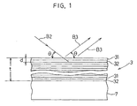
- this spectroscopic device is a multilayered spectroscopic device 3 for use in fluorescent X-ray analysis of boron (B) contained in a sample, which device includes a substrate 7 in the form of a silicon wafer on which a plurality of layer pairs each pair including a reflecting layer 31 made of lanthanum (La) and a spacer layer 32 made of boron (B) are formed in a stacked fashion by means of an ion beam sputtering film forming technique.
- secondary X-rays B2 such as fluorescent X-rays emitted from the sample are incident at a predetermined angle of incidence (angle of diffraction) ⁇ and B-K ⁇ line B3 representative of the fluorescent X-rays emitted from boron are reflected (diffracted or dispersed) at an angle equal to the angle of incidence ⁇ .
- the material that can be employed for the reflecting layers 31 may include an alloy containing lanthanum as a principal component mixed with molybdenum (Mo) or ruthenium (Ru), or a lanthanum oxide (La 2 O 3 ). Some examples of use of those different materials for the reflecting layers 31 will be discussed later.
- boron is a semiconductor that can be substantially regarded as a dielectric material and, therefore, unlike boron carbide (B 4 C) that has been used as a material for the conventional spacer layers and that is considered a good electroconductive material, film forming by the use of any standard deposition technique has been considered difficult to achieve and it has been considered extremely difficult to secure an extremely thin film having a sufficiently small roughness.
- the present invention is not always limited to the use of the ion beam sputtering film forming technique, but any other suitable film forming technique such as a high frequency magnetron sputtering technique or a laser beam deposition technique can be equally employed.
- the film thickness ratio of the reflecting layer 31 relative to the spacer layer 32 is chosen to be 1 by the following reason.
- Table 1 five La/B based multilayered spectroscopic devices were prepared and for each of those spectroscopic devices the strength of reflection of B-K ⁇ line was measured, followed by calculation of the reflection strength ratio (the relative reflection strength) with the conventional Mo/B 4 C based multilayered spectroscopic device.
- one conventional La/B 4 C based multilayered spectroscopic device was prepared and the strength of reflection of B-K ⁇ line was similarly measured, followed by calculation of the reflection strength ratio (the relative reflection strength) with the conventional Mo/B 4 C based multilayered spectroscopic device.
- the relative reflection strength is large when the periodic length, representative of the thickness of a single layer pair, is chosen to be 8 nm, the number of the layer pairs is chosen to be not smaller than 30, as is the case with the conventional Mo/B 4 C based multilayered spectroscopic device (Compare the top three rows in Table 1), and the film thickness ratio of the reflecting layers 31 relative to the spacer layers 32 is chosen to be 1:1, rather than 1:2 that is used in the conventional multilayered spectroscopic device.
- the film thickness ratio of the reflecting layers 31 relative to the spacer layers 32 is preferred to be 1:1. It is to be noted that unlike the conventional case, selection of the film thickness ratio in the practice of the present invention is not always critical by the reason which will be described later.
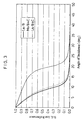
- the film thickness ratio is chosen to be 1:1 and the number of the layer pairs is chosen to be within the range of 15 to 40 is plotted in a chart, it will readily be seen from the chart of Fig. 2 that the relative reflection strength substantially saturates when the number of the layer pairs is chosen to be 35. In other words, when the number of the layer pairs is chosen to be 35, the strength of reflection of B-K ⁇ line will be 98% of the saturation value exhibited when the number of the layer pairs is 40. Saturation of the reflection strength is affected only by the total laminated film thickness t (Fig.
- the present invention chooses the total laminated film thickness t (corresponding to a value equal to or higher than 280 nm) at which the strength of reflection of B-K ⁇ line attains a value not lower than 98% (i.e., quite naturally lower than 100%) of the saturation value, so that the strength of reflection of B-K ⁇ can be increased for the purpose of the present invention.
- the number of the layer pairs when the periodic length is 8 nm suffices to be within the range of 35 to 40 and, hence, the total laminated film thickness t is preferably within the range of 280 to 320 nm.
- the periodic length of the Mo/B 4 C based multilayered spectroscopic device is generally about 8 nm and in such case the angle of incidence of a peak of B-K ⁇ line would be about 25°. If the reflectance of Si-L line at such angle is taken as a target value, the angle of incidence achieved with the La/B based multilayered spectroscopic device at which the reflectance of Si-L line attains a value about equal to the target reflectance would be about 14°.
- the periodic length d of the La/B based multilayered spectroscopic device according to the present invention will be 14 nm at maximum if the reflectance of Si-L line can be tolerated to a value about equal to that exhibited by the conventional Mo/B 4 C based multilayered spectroscopic device.
- the periodic length d that is to be employed in the practice of the present invention is preferred to be within the range of 7 to 14 nm.
- the film thickness ratio of the reflecting layers 31 relative to the spacer layers 32 is appropriately chosen to 1:1 in order to increase the strength of reflection of B-K ⁇ line by the reasons as hereinbefore discussed, a question would arise that if the film thickness ratio is chosen to be 1:1 in the multilayered spectroscopic device of the present invention, the third order reflection of O-K line will bring about undesirable influences more considerable than that with the conventional multilayered spectroscopic device.
- the La/B based multilayered spectroscopic device of the present invention is such that the film thickness ratio of the reflecting layers 31 relative to the spacer layers 32 need not be specifically set in order to reduce the third order reflection of O-K line.
- the film thickness ratio of the reflecting layers 31 relative to the spacer layers 32 may not be strictly 1, but may be sufficiently within the range of 2/3 to 3/2 and preferably within the range of 4/5 to 5/4.
- the periodic length d is chosen to be within the range of 7 to 14 nm and the film thickness ratio of the reflecting layers 31 relative to the spacer layers 32 is chosen to be within the range of 2/3 to 3/2 and preferably 4/5 and 5/4. If in a condition in which the periodic length d and the film thickness ratio are determined, the total laminated film thickness t is increased, the strength of reflection of B-K ⁇ line will increase and be eventually saturated, and accordingly the total laminated film thickness t is chosen to be a value equal to or higher than 98% of the saturation value of the reflection strength and, preferably, within the range of 280 to 320 nm. According to Table 1 and Fig.
- the film thickness ratio is chosen to be 1 and the total laminated film thickness is chosen to be within the range of 280 to 320 nm (corresponding to the use of 35 to 40 layer pairs), the strength of reflection of B-K ⁇ is about 2.2 times that exhibited by the conventional Mo/B 4 C based multilayered spectroscopic device and, on the other hand, in the embodiment in which the periodic length is chosen to be 13 nm, the film thickness ratio is chosen to be 1 and the total laminated film thickness is chosen to be 312 nm (corresponding to the use of 24 layer pairs), the strength of reflection of B-K ⁇ is about 3.8 times that exhibited by the conventional Mo/B 4 C based multilayered spectroscopic device.
- the influences brought about respectively by the third order reflection of O-K line that provide the interfering X-rays and Si-L line that provide the background can be sufficiently reduced simultaneously.
- a spectroscopic device in which the periodic length is 8 nm, the film thickness ratio is 1:1 and the total laminated film thickness is 320 nm (corresponding to the use of 40 layer pairs) was prepared in the same manner as hereinbefore described.
- La 2 O 3 /B based multilayered spectroscopic device it has been found that as compared with the previously discussed La/B based multilayered spectroscopic device having the same periodic length and other numerical values, the strength of reflection of B-K ⁇ has been found substantially identical.
- the influences brought about respectively by the third order reflection of O-K line that provide the interfering X-rays and Si-L line that provide the background can be reduced by a quantity similar to that with the La/B based multilayered spectroscopic device.
- the La 2 O 3 /B based and La/B based multilayered spectroscopic devices in those respective embodiments and the conventional La/B 4 C based multilayered spectroscopic device were tested as to their durability under a high humidity atmosphere of a 100% relative humidity.
- the multilayered spectroscopic device for use in fluorescent X-ray analysis of boron As discussed in the foregoing, with the multilayered spectroscopic device for use in fluorescent X-ray analysis of boron according to the present invention, as compared with the conventional Mo/B 4 C based multilayered spectroscopic device, not only can the influences brought about respectively by the third order reflection of O-K line that provide the interfering X-rays and Si-L line that provide the background be reduced sufficiently, but also the strength of reflection of B-K ⁇ line can be increased to a value that is about 2.2 to 3.8 times that exhibited by the conventional multilayered spectroscopic device and, even compared with the conventional La/B 4 C based multilayered spectroscopic device, the strength of reflection of B-K ⁇ can be increased to a value that is by a factor of about 1.3 and, therefore, the fluorescent X-ray analysis of boron can be achieved highly accurately in a short length of time.
Landscapes
- Physics & Mathematics (AREA)
- Engineering & Computer Science (AREA)
- Chemical & Material Sciences (AREA)
- Spectroscopy & Molecular Physics (AREA)
- Nanotechnology (AREA)
- High Energy & Nuclear Physics (AREA)
- General Engineering & Computer Science (AREA)
- Analytical Chemistry (AREA)
- Immunology (AREA)
- Pathology (AREA)
- General Physics & Mathematics (AREA)
- General Health & Medical Sciences (AREA)
- Biochemistry (AREA)
- Life Sciences & Earth Sciences (AREA)
- Mathematical Physics (AREA)
- Theoretical Computer Science (AREA)
- Crystallography & Structural Chemistry (AREA)
- Health & Medical Sciences (AREA)
- Analysing Materials By The Use Of Radiation (AREA)
Abstract
Description
| Materials for Multilayered Spectroscopic Devices | Cycle Length (nm) | Film Thickness Ratio (La:B) | Number of Layer Pairs (pairs) | Relative Reflection Strength (as compared with the Convention) |
| La/B | 8 | 1:2 | 45 | 1.82 |
| 8 | 1:1 | 40 | 2.21 | |
| 8 | 1:1 | 30 | 2.13 | |
| 8 | 1:1 | 15 | 1.66 | |
| 13 | 1:1 | 24 | 3.77 | |
| La/B4C | 8 | 1:1 | 40 | 1.74 |
Claims (3)
- A multilayered spectroscopic device for use in fluorescent X-ray analysis of boron (B) contained in a sample, which device comprises a plurality of layer pairs, each pair including a reflecting layer and a spacer layer, that are laminated on a substrate;
wherein lanthanum (La), an alloy containing lanthanum as a principal component or lanthanum oxide (La2O3) is used as material for the reflecting layers, and boron is used as material for the spacer layers, a periodic length is chosen to be within the range of 7 to 14 nm and a film thickness ratio of the reflecting layers relative to the spacer layers is chosen to be within the range of 2/3 to 3/2; and
wherein the multilayered spectroscopic device has a total laminated film thickness sufficient to allow a strength of reflection of B-Kα line to attain a value equal to or higher than 98% of a saturation value. - The multilayered spectroscopic device for use in fluorescent X-ray analysis of boron as claimed in Claim 1, wherein the total laminated film thickness is chosen to be within the range of 280 to 320 nm.
- The multilayered spectroscopic device for use in fluorescent X-ray analysis of boron as claimed in Claim 1, wherein the film thickness ratio of the reflecting layers relative to the spacer layer is chosen to be within the range of 4/5 to 5/4.
Applications Claiming Priority (5)
| Application Number | Priority Date | Filing Date | Title |
|---|---|---|---|
| JP2001175642 | 2001-06-11 | ||
| JP2001175642 | 2001-06-11 | ||
| JP2002032537 | 2002-02-08 | ||
| JP2002032537A JP3600849B2 (en) | 2001-06-11 | 2002-02-08 | Multilayer spectroscopy device for boron X-ray fluorescence analysis |
| PCT/JP2002/005317 WO2002101368A1 (en) | 2001-06-11 | 2002-05-30 | Multi-layer film spectroscopic element for boron fluorescence x-ray analysis |
Publications (3)
| Publication Number | Publication Date |
|---|---|
| EP1318393A1 true EP1318393A1 (en) | 2003-06-11 |
| EP1318393A4 EP1318393A4 (en) | 2008-12-17 |
| EP1318393B1 EP1318393B1 (en) | 2010-10-20 |
Family
ID=26616694
Family Applications (1)
| Application Number | Title | Priority Date | Filing Date |
|---|---|---|---|
| EP02730818A Expired - Lifetime EP1318393B1 (en) | 2001-06-11 | 2002-05-30 | Multi-layer film spectroscopic element for boron fluorescence x-ray analysis |
Country Status (7)
| Country | Link |
|---|---|
| US (1) | US6836533B2 (en) |
| EP (1) | EP1318393B1 (en) |
| JP (1) | JP3600849B2 (en) |
| DE (1) | DE60238025D1 (en) |
| MY (1) | MY131146A (en) |
| TW (1) | TW583394B (en) |
| WO (1) | WO2002101368A1 (en) |
Cited By (1)
| Publication number | Priority date | Publication date | Assignee | Title |
|---|---|---|---|---|
| EP2772752A4 (en) * | 2011-10-28 | 2015-09-02 | Hamamatsu Photonics Kk | X-RAY SPECTROMETRY DETECTOR DEVICE |
Families Citing this family (9)
| Publication number | Priority date | Publication date | Assignee | Title |
|---|---|---|---|---|
| US7003758B2 (en) * | 2003-10-07 | 2006-02-21 | Brion Technologies, Inc. | System and method for lithography simulation |
| JP4466566B2 (en) * | 2003-10-15 | 2010-05-26 | 株式会社ニコン | MULTILAYER REFLECTOR, MULTILAYER REFLECTOR MANUFACTURING METHOD, AND EXPOSURE APPARATUS |
| DE102008040265A1 (en) * | 2008-07-09 | 2010-01-14 | Carl Zeiss Smt Ag | Reflective optical element and method for its production |
| JP2012222349A (en) * | 2011-04-05 | 2012-11-12 | Asml Netherlands Bv | Multilayer mirror and lithographic apparatus |
| JP5951010B2 (en) * | 2011-06-15 | 2016-07-13 | エーエスエムエル ネザーランズ ビー.ブイ. | Multilayer mirror, method for producing multilayer mirror and lithographic apparatus |
| DE102013210533A1 (en) * | 2013-06-06 | 2014-12-11 | Carl Zeiss Smt Gmbh | MIRROR FOR BEUV LIGHT |
| JP6142135B2 (en) * | 2014-12-25 | 2017-06-07 | 株式会社リガク | Obliquely incident X-ray fluorescence analyzer and method |
| CN105136831B (en) * | 2015-08-28 | 2016-06-22 | 钢研纳克检测技术有限公司 | A kind of rare-earth smelting separation process quality partition amount on-line computing model |
| GB2547183B (en) * | 2015-12-14 | 2021-08-25 | Trichord Ltd | Printing on to a 3-dimensional article |
Family Cites Families (17)
| Publication number | Priority date | Publication date | Assignee | Title |
|---|---|---|---|---|
| US4785470A (en) * | 1983-10-31 | 1988-11-15 | Ovonic Synthetic Materials Company, Inc. | Reflectivity and resolution X-ray dispersive and reflective structures for carbon, beryllium and boron analysis |
| JPH07113679B2 (en) * | 1986-03-28 | 1995-12-06 | 日本電信電話株式会社 | Multilayer film mirror |
| US5310603A (en) * | 1986-10-01 | 1994-05-10 | Canon Kabushiki Kaisha | Multi-layer reflection mirror for soft X-ray to vacuum ultraviolet ray |
| JPH0534500A (en) * | 1991-08-02 | 1993-02-09 | Olympus Optical Co Ltd | X-ray multilayered film reflecting mirror |
| US5265143A (en) * | 1993-01-05 | 1993-11-23 | At&T Bell Laboratories | X-ray optical element including a multilayer coating |
| DE4402113A1 (en) * | 1994-01-26 | 1995-07-27 | Geesthacht Gkss Forschung | Method and arrangement for determining elements using the method of total reflection X-ray fluorescence analysis |
| JP3034420B2 (en) * | 1994-02-21 | 2000-04-17 | 理学電機工業株式会社 | Background correction method for X-ray fluorescence analysis |
| US5485499A (en) * | 1994-08-05 | 1996-01-16 | Moxtek, Inc. | High throughput reflectivity and resolution x-ray dispersive and reflective structures for the 100 eV to 5000 eV energy range and method of making the devices |
| JPH1138192A (en) * | 1997-07-17 | 1999-02-12 | Nikon Corp | Multilayer reflector |
| JP3602717B2 (en) * | 1998-03-11 | 2004-12-15 | エヌ・ティ・ティ・アドバンステクノロジ株式会社 | Multi-layer X-ray reflector |
| JPH11295245A (en) * | 1998-04-10 | 1999-10-29 | Rigaku Industrial Co | X-ray spectroscopic element and x-ray analysis apparatus using the same |
| JP2000147999A (en) | 1998-11-06 | 2000-05-26 | Matsushita Electric Ind Co Ltd | How to use a speech learning system and learning speech materials |
| JP2000147197A (en) * | 1998-11-13 | 2000-05-26 | Rigaku Industrial Co | Multilayer spectroscopic element for boron X-ray fluorescence analysis |
| JP2000147199A (en) * | 1998-11-13 | 2000-05-26 | Rigaku Industrial Co | Multilayer spectroscopy device for beryllium X-ray fluorescence analysis |
| JP2000241593A (en) * | 1999-02-22 | 2000-09-08 | Rigaku Industrial Co | Multilayer spectroscopic element for X-ray fluorescence analysis of carbon |
| DE19926056B4 (en) * | 1999-06-08 | 2004-03-25 | Gkss-Forschungszentrum Geesthacht Gmbh | Device for analyzing atomic and / or molecular elements using wavelength-dispersive, X-ray spectrometric devices |
| US6396900B1 (en) * | 2001-05-01 | 2002-05-28 | The Regents Of The University Of California | Multilayer films with sharp, stable interfaces for use in EUV and soft X-ray application |
-
2002
- 2002-02-08 JP JP2002032537A patent/JP3600849B2/en not_active Expired - Fee Related
- 2002-05-30 EP EP02730818A patent/EP1318393B1/en not_active Expired - Lifetime
- 2002-05-30 WO PCT/JP2002/005317 patent/WO2002101368A1/en not_active Ceased
- 2002-05-30 US US10/258,845 patent/US6836533B2/en not_active Expired - Lifetime
- 2002-05-30 DE DE60238025T patent/DE60238025D1/en not_active Expired - Lifetime
- 2002-06-03 TW TW091111820A patent/TW583394B/en not_active IP Right Cessation
- 2002-06-04 MY MYPI20022051A patent/MY131146A/en unknown
Cited By (1)
| Publication number | Priority date | Publication date | Assignee | Title |
|---|---|---|---|---|
| EP2772752A4 (en) * | 2011-10-28 | 2015-09-02 | Hamamatsu Photonics Kk | X-RAY SPECTROMETRY DETECTOR DEVICE |
Also Published As
| Publication number | Publication date |
|---|---|
| TW583394B (en) | 2004-04-11 |
| US20040022354A1 (en) | 2004-02-05 |
| WO2002101368A1 (en) | 2002-12-19 |
| MY131146A (en) | 2007-07-31 |
| JP2003065979A (en) | 2003-03-05 |
| EP1318393A4 (en) | 2008-12-17 |
| EP1318393B1 (en) | 2010-10-20 |
| US6836533B2 (en) | 2004-12-28 |
| DE60238025D1 (en) | 2010-12-02 |
| JP3600849B2 (en) | 2004-12-15 |
Similar Documents
| Publication | Publication Date | Title |
|---|---|---|
| US7848483B2 (en) | Magnesium silicide-based multilayer x-ray fluorescence analyzers | |
| US20050036583A1 (en) | X-ray fluorescence system with apertured mask for analyzing patterned surfaces | |
| EP2010963B1 (en) | Reflective mask blank for euv lithography | |
| US6836533B2 (en) | Multi-layer film spectroscopic element for boron fluorescene X-ray analysis | |
| KR20040072780A (en) | Method for measuring a thickness of a thin layer | |
| EP2708846B1 (en) | Method for determining film thickness of soi layer of soi wafer | |
| TWI329736B (en) | X-ray scattering with a polychromatic source | |
| US6628748B2 (en) | Device and method for analyzing atomic and/or molecular elements by means of wavelength dispersive X-ray spectrometric devices | |
| Schwenke et al. | How to use the features of total reflection of X-rays for energy dispersive XRF | |
| EP1390957B1 (en) | Multi-layer mirror for radiation in the xuv wavelenght range and method for manufacture thereof | |
| JP2589638B2 (en) | X-ray fluorescence analysis method and apparatus | |
| Andermann | Surface-film and interfacial analysis via variable grazing exit angle x-ray fluorescence spectrometry | |
| JP3185825B2 (en) | Standard sample | |
| JPH0792112A (en) | X-ray evaluation device | |
| JP3545966B2 (en) | Multilayer thin film composition measurement method | |
| JP3188393B2 (en) | Multilayer spectroscopy element | |
| JP2000241593A (en) | Multilayer spectroscopic element for X-ray fluorescence analysis of carbon | |
| US20030169845A1 (en) | X-ray monochromator and X-ray fluorescence spectrometer using the same | |
| JPS63191951A (en) | X-ray spectral element | |
| JPH04223210A (en) | Method for measuring film thickness of multilayer film | |
| JP2000147197A (en) | Multilayer spectroscopic element for boron X-ray fluorescence analysis | |
| Vrebos et al. | ACXRI'96 ADVANCES IN LOW ATOMIC NUMBER ELEMENT ANALYSIS BY WAVELENGTH DISPERSIVE X-RAY FLUORESCENCE SPECTROMETRY | |
| WO2025224607A1 (en) | Large scale monochromator | |
| Knoll et al. | Multilayer reflectors for improving the primary beam intensity: Reflectivity measurements on coated glasses | |
| Wählisch et al. | Interlaboratory comparison of XRF analysis on thin films, including alloys, oxides, multilayers, and a lithium-ion battery material |
Legal Events
| Date | Code | Title | Description |
|---|---|---|---|
| PUAI | Public reference made under article 153(3) epc to a published international application that has entered the european phase |
Free format text: ORIGINAL CODE: 0009012 |
|
| AK | Designated contracting states |
Designated state(s): AT BE CH CY DE DK ES FI FR GB GR IE IT LI LU MC NL PT SE TR |
|
| AX | Request for extension of the european patent |
Extension state: AL LT LV MK RO SI |
|
| 17P | Request for examination filed |
Effective date: 20030428 |
|
| A4 | Supplementary search report drawn up and despatched |
Effective date: 20081117 |
|
| RAP1 | Party data changed (applicant data changed or rights of an application transferred) |
Owner name: RIGAKU CORPORATION |
|
| 17Q | First examination report despatched |
Effective date: 20090623 |
|
| GRAP | Despatch of communication of intention to grant a patent |
Free format text: ORIGINAL CODE: EPIDOSNIGR1 |
|
| RBV | Designated contracting states (corrected) |
Designated state(s): DE |
|
| GRAS | Grant fee paid |
Free format text: ORIGINAL CODE: EPIDOSNIGR3 |
|
| RIN1 | Information on inventor provided before grant (corrected) |
Inventor name: SHIMIZU, KAZUAKI,C/O RIGAKU CORPORATION |
|
| GRAA | (expected) grant |
Free format text: ORIGINAL CODE: 0009210 |
|
| AK | Designated contracting states |
Kind code of ref document: B1 Designated state(s): DE |
|
| REF | Corresponds to: |
Ref document number: 60238025 Country of ref document: DE Date of ref document: 20101202 Kind code of ref document: P |
|
| PLBE | No opposition filed within time limit |
Free format text: ORIGINAL CODE: 0009261 |
|
| STAA | Information on the status of an ep patent application or granted ep patent |
Free format text: STATUS: NO OPPOSITION FILED WITHIN TIME LIMIT |
|
| 26N | No opposition filed |
Effective date: 20110721 |
|
| REG | Reference to a national code |
Ref country code: DE Ref legal event code: R097 Ref document number: 60238025 Country of ref document: DE Effective date: 20110721 |
|
| PGFP | Annual fee paid to national office [announced via postgrant information from national office to epo] |
Ref country code: DE Payment date: 20170124 Year of fee payment: 16 |
|
| REG | Reference to a national code |
Ref country code: DE Ref legal event code: R119 Ref document number: 60238025 Country of ref document: DE |
|
| PG25 | Lapsed in a contracting state [announced via postgrant information from national office to epo] |
Ref country code: DE Free format text: LAPSE BECAUSE OF NON-PAYMENT OF DUE FEES Effective date: 20181201 |