EP1317014A1 - Filter circuit and high frequency communication circuit using the same - Google Patents
Filter circuit and high frequency communication circuit using the same Download PDFInfo
- Publication number
- EP1317014A1 EP1317014A1 EP01943796A EP01943796A EP1317014A1 EP 1317014 A1 EP1317014 A1 EP 1317014A1 EP 01943796 A EP01943796 A EP 01943796A EP 01943796 A EP01943796 A EP 01943796A EP 1317014 A1 EP1317014 A1 EP 1317014A1
- Authority
- EP
- European Patent Office
- Prior art keywords
- filter
- line
- filter circuit
- lines
- capacitive
- Prior art date
- Legal status (The legal status is an assumption and is not a legal conclusion. Google has not performed a legal analysis and makes no representation as to the accuracy of the status listed.)
- Withdrawn
Links
Images


Classifications
-
- H—ELECTRICITY
- H01—ELECTRIC ELEMENTS
- H01P—WAVEGUIDES; RESONATORS, LINES, OR OTHER DEVICES OF THE WAVEGUIDE TYPE
- H01P1/00—Auxiliary devices
- H01P1/20—Frequency-selective devices, e.g. filters
- H01P1/201—Filters for transverse electromagnetic waves
- H01P1/203—Strip line filters
- H01P1/20327—Electromagnetic interstage coupling
- H01P1/20354—Non-comb or non-interdigital filters
- H01P1/20381—Special shape resonators
-
- H—ELECTRICITY
- H01—ELECTRIC ELEMENTS
- H01P—WAVEGUIDES; RESONATORS, LINES, OR OTHER DEVICES OF THE WAVEGUIDE TYPE
- H01P1/00—Auxiliary devices
- H01P1/20—Frequency-selective devices, e.g. filters
- H01P1/201—Filters for transverse electromagnetic waves
- H01P1/2013—Coplanar line filters
-
- H—ELECTRICITY
- H01—ELECTRIC ELEMENTS
- H01P—WAVEGUIDES; RESONATORS, LINES, OR OTHER DEVICES OF THE WAVEGUIDE TYPE
- H01P1/00—Auxiliary devices
- H01P1/20—Frequency-selective devices, e.g. filters
- H01P1/201—Filters for transverse electromagnetic waves
- H01P1/205—Comb or interdigital filters; Cascaded coaxial cavities
- H01P1/2053—Comb or interdigital filters; Cascaded coaxial cavities the coaxial cavity resonators being disposed parall to each other
Definitions
- the present invention relates to a filter circuit and a high frequency communication circuit device using the same, and more particularly to a filter circuit selectively passing a predetermined frequency component of a signal input to an input terminal to an output terminal and a high frequency communication circuit device using the same.
- Fig. 18 is a perspective view showing a configuration of an edge coupled filter as a representative distributed constant filter.
- This filter is provided for a micro-strip line that is most common as a distributed constant line.
- this filter includes a substrate 150 formed of an insulator such as alumina ceramic.
- a ground layer 151 is formed on the entire back surface of substrate 150.
- Lines 152 and 153 are part of the micro-strip line as a high frequency transmission line and respectively form an input terminal and an output terminal for the filter.
- Lines 154 and 155 form so-called ⁇ /2 open line resonators.
- ⁇ is a wavelength of the electrical signal transmitted through the line, in the frequency in the vicinity of the center frequency of the filter circuit.
- micro-strip lines 152 and 153 and ⁇ /2 open line resonators 154 and 155 are collectively patterned with high accuracy on the surface of insulator substrate 150 by means of print or photolithography. Therefore the planar circuit filter having the structure in Fig. 18 is generally known as a filter circuit with low cost and with excellent productivity.
- a distributed constant type filter circuit formed of micro-strip lines as shown in Fig. 18 will mainly be described in the present specification.
- the effect of the present invention is not limited to such a filter. It can readily be applied to a filter circuit formed of a coplanar line or a semi-concentrated constant type filter with a part of circuit elements replaced with concentrated constant discrete components.
- a planar view of a substrate seen from above will be shown as a view showing the structure of the distributed constant filter, for the sake of brevity, in the present specification.
- Figs. 19A and 19B Equivalent circuits having the structure of Fig. 18 are shown in Figs. 19A and 19B.
- the equivalent circuit is shown in two stages to facilitate understanding.
- Fig. 19A is an equivalent circuit that is represented with great use of distributed constant line in a one-to-one correspondence with the structure of Fig. 18.
- the equivalent circuit including a distributed constant line as shown in Fig. 19A is inconvenient in a later simulation. Assuming that calculation is made using a commercially available high frequency circuit simulator, the calculation results somewhat vary depending products and manufactures and methods of defining parameters are so varied to understand.
- an equivalent circuit with only concentrated constant in Fig. 19B is illustrated together, and the simulation is mainly performed using the equivalent circuit with only concentrated constant.
- Figs. 19A and 19B are equivalent in the vicinity of resonance frequency of the filter. This is because a ⁇ /2 open line resonator is equivalent to an LC parallel resonance circuit having one end grounded in the vicinity of its resonance frequency.
- an LC parallel resonance circuit 154 including a coil 154a and a capacitor 154B having one end grounded and an LC parallel resonance circuit 155 including a coil 155a and a capacitor 155b having one end grounded correspond to ⁇ /2 open line resonators 154 and 155 in Fig. 18, respectively.
- Each of coils 154a and 155b has a prescribed inductance L1 and each of capacitors 154b and 155b has a prescribed capacitance C1. This is because, in the resonance frequency, the middle portion of the ⁇ /2 open line resonator is equivalently grounded and the impedance is close to infinity at both open ends.
- 19A and 19B correspond to electromagnetic field coupling portions 156 and 157 in Fig. 18.
- electromagnetic field coupling portions 156 and 157 micro-strip lines 152 and 153 and ⁇ /2 open line resonators 154 and 155 are arranged closely spaced apart from each other at the open ends approximately by ⁇ /4 or less.
- Capacitor 158 having a capacitance C3 in Figs. 19A and 19B corresponds to an electromagnetic field coupling portion 158 in Fig. 18.
- lines 154 and 155 are arranged close to each other at the open ends. In this case, it is known that electromagnetic field coupling occurs based on capacitive coupling.
- the present invention aims at a filter circuit for use in extremely high frequency band such as millimeter wave band, in particular.
- An exemplary equivalent circuit in Fig. 19B that is optimally designed for 60 GHz band is shown.
- Figs. 20A and 20B are frequency characteristics graphs of that filter.
- the axis of abscissas represents the frequency [GHz] and the axis of ordinates represent the absolute value of S parameters expressed in dB.
- Figs. 20A and 20B the axis of abscissas represents the frequency [GHz] and the axis of ordinates represent the absolute value of S parameters expressed in dB.
- Figs. 20A and 20B the axis of abscissas represents
- Fig. 20A shows the characteristics of the wide band
- Fig. 20B shows the characteristics of the vicinity of the passband.
- the filter having the structure in Fig. 18 functions as a bandpass filter.
- the graphs in the formats shown in Figs. 20A and 20B will be used to express the filter characteristics. Furthermore, in the present specification, the operation principle of the filter will be described, as shown in Figs. 18 - 20B, by first showing the structure, then showing the equivalent circuit thereof, and finally showing the calculation result of the filter characteristics of the equivalent circuit. It is noted that in a second embodiment of the present invention, the effectiveness of the present invention is validated by showing the measurement result of the filter that was actually prototyped rather than only by calculation results.
- Bandpass filters with high steepness are in the greatest demand among the filters.
- filters with high steepness are essential, as the passband is in the close vicinity of the attenuation band.
- the filter of Fig. 18 results in the filter characteristics that are gradual with poor steepness as shown in Figs. 20A and 20B, without some special scheme. Then, in order to improve the steepness of such a bandpass filter, the design method of creating attenuation poles at the frequencies immediately above and below the passband has been developed.
- a circuit shown in Fig. 21 has been known as a circuit that achieves satisfactory results in the extremely high frequency band such as the millimeter wave band and has a simple structure for facilitating design ("Low Loss Micromachined Filters For Millimeter-Wave Telecommunication Systems", Pierre Blondy et al., 1998 IEEE MTT-S Digest, pp. 1181-1184).
- this filter includes an insulator substrate 161 formed of alumina ceramic or the like, micro-strip lines 162 and 163 formed on the surface thereof, and ⁇ /2 open line resonators 164 and 165. Portions 167 - 170 enclosed by dotted lines are portions where lines 162 - 165 are close to each other to cause electromagnetic field coupling.
- MTT-S Digest the aforementioned reference
- the aforementioned reference describes both of a filter (two-pole filter) having two ⁇ /2 open line resonators and a filter (four-pole filter) having four ⁇ /2 open line resonators.
- the effect of the invention will be discussed in vain unless the filters are compared under the same conditions.
- the discussion in the present specification is consistently based on the filter (two-pole filter) having two ⁇ /2 open line resonators, for the sake of brevity.
- Figs. 22A and 22B are circuit diagrams showing the equivalent circuit of the filter in Fig. 21.
- Fig. 22A is an equivalent circuit with great use of distributed constant line
- Fig. 22B is an equivalent circuit represented with only distributed constant.
- an LC parallel resonance circuit 164 including a coil 164a and a capacitor 164b having one end grounded and an LC parallel resonance circuit 165 including a coil 165a and a capacitor 165b having one end grounded correspond to ⁇ /2 open line resonators 164 and 165 in Fig. 21, respectively.
- Each of coils 164a and 165a has a prescribed inductance L1 and each of capacitors 164b and 165b has a prescribed capacitance C1.
- Capacitors 168 and 169 having a capacitance C2 in Figs. 22A and 22B correspond to electromagnetic field coupling portions 168 and 169 in Fig. 21, respectively.
- a capacitor 167 having a capacitance C3 in Figs. 22A and 22B corresponds to an electromagnetic field coupling portion 167 in Fig. 21.
- the coefficient of mutual induction coupling K of Figs. 22A and 22B corresponds to an electromagnetic field coupling portion 170 in Fig. 21.
- electromagnetic field coupling portion 170 the middle portions of two ⁇ /2 open line resonators 164 and 165, that is, the portions where the current is maximum are arranged to align closely parallel to each other. In this case, it is known that electromagnetic field coupling based on mutual inductive magnetic field coupling occurs.
- S21 in Fig. 23A is -50 dB or below.
- S21 in Fig. 20A is -17 dB whereas S21 in Fig. 23A is -50dB or below.
- the filter characteristics in Figs. 23A and 23B are more advantageous than the filter characteristics of Figs. 20A and 20B, as it provides more attenuation amount.
- the filter of the equivalent circuit in Fig. 22A, 22B is a commonly known circuit configuration and is described in many references. For example, it is described in the second chapter of "Design and Application of Communication Filter Circuit” (edited and authored by Yoshihiro Konishi, Sogo Denshi Shuppan), which is a prominent text book of the high frequency filter technique.
- the conventional filter has the problem in that the steepness of the filter is not sufficient when it is used in a radio communication device for the extremely high frequency band such as the millimeter wave band, in particular.
- the steepness of the filter characteristics becomes high.
- the steepness of the graph in Figs. 23A and 23B approaches its limit, which can be confirmed easily with a common circuit simulation.
- the frequencies at the attenuation poles can be set only at the frequencies as far as 15 % or more apart when represented as being standardized by the center frequency. If the attenuation poles are forced to be closer, the waveform of the filter characteristics is distorted.
- the conventional filter having the characteristics of Figs. 23A and 23B is sufficient as long as the local frequency is positioned at 48 GHz relative to the center frequency 60 GHz.
- the local frequency is often positioned at the frequency closer to the center frequency 60 GHz, for example 57 GHz or 58 GHz. In such a case, with the conventional filter, the steepness is not sufficient and the attenuation amount cannot be assured.
- the steepness of the filter varies depending on the minute condition settings such as specific bandwidth or attenuation amount.
- the frequencies at the attenuation poles successively come to close at more than 8 % when represented as being standardized by the center frequency.
- the steepness of the filter is easier to understand in its effect in the discussion of the somewhat wider band.
- the present invention is made to solve the problems described above and the object is to provide a filter circuit having steep filter characteristics.
- a filter circuit includes: a plurality of resonators wherein an impedance between respective input/output terminals and a reference potential line is maximum in each resonance frequency and each input/output terminal is capacitive-coupled to at least one of other input/output terminals; first capacitive coupling means for capacitive-coupling input/output terminals of any two resonators of the plurality of resonators and first and second terminals respectively to each other; and electromagnetic field coupling means for connecting the first and second terminals respectively to the input terminal and the output terminal and bringing the input terminal and the output terminal into magnetic field coupling by mutual induction. Therefore the frequency at an attenuation pole can be close to a center frequency without degrading the waveform of the filter characteristics and the steepness of the filter characteristics can be increased.
- second capacitive coupling means for capacitive-coupling the input terminal and the output terminal to each other is further included.
- the number of attenuation poles can be increased and an attenuation amount of the cut-off band can be increased.
- the filter circuit is formed of a line pattern made of a conductor formed on an insulator substrate.
- Each of the plurality of resonators includes a first line having a predetermined line length. At least one end portion of both end portions of each first line is capacitive-coupled to one end portion of another first line.
- the first capacitive coupling means includes third and fourth lines having respective one end portions capacitive-coupled to the other end portions of two first lines included in the two resonators and having respective other end portions connected to the first and second terminals.
- the electromagnetic field coupling means includes fifth and sixth lines connected between the first and second terminals and the input terminal and the output terminal, respectively, each having at least a part arranged parallel to the other in proximity.
- the filter circuit can be realized with a planar print circuit thereby allowing for reduction in size and cost of the circuit.
- a filter circuit includes: a plurality of resonators wherein an impedance between respective input/output terminals and a reference potential line is maximum in each resonance frequency and each input/output terminal is capacitive-coupled to at least one of other input/output terminals; first capacitive coupling means for capacitive-coupling input/output terminals of any two resonators of the plurality of resonators and first and second terminals respectively to each other; electromagnetic field coupling means for connecting the first and second terminals respectively to the input terminal and the output terminal and bringing the input terminal and the output terminal into magnetic field coupling by mutual induction; and second capacitive coupling means for capacitive-coupling the input terminal and the output terminal to each other.
- Each of the plurality of resonators includes a first line having a predetermined line length. At least one end portion of both end portions of each first line is capacitive-coupled to one end portion of another first line.
- the first capacitive coupling means includes third and fourth lines having respective one end portions capacitive-coupled to the other end portions of two first lines included in the two resonators and having respective other end portions connected to the first and second terminals.
- the electromagnetic field coupling means includes fifth and sixth lines having respective one end portions respectively connected to the first and second terminals, each having at least a part arranged parallel to the other in proximity.
- the second capacitive coupling means includes seventh and eighth lines connected between the other end portions of the fifth and sixth lines and the input terminal and the output terminal, respectively, and each having at least a part arranged proximate to the other. Therefore the frequency at the attenuation pole can be close to the center frequency without degrading the waveform of the filter characteristics and the steepness of the filter characteristics can be increased. Moreover, the filter circuit can be realized with a planar print circuit thereby allowing for reduction in size and cost of the circuit.
- the fifth and sixth lines are proximate to each other at a position of a quarter wave of a signal having a center frequency of the filter circuit from open ends of the third and fourth lines.
- the current value is maximum in the fifth and sixth lines, the mutual inductive magnetic field coupling between the fifth and sixth lines can be created in a limited space efficiently.
- each of the plurality of resonators is a quarter wave short-circuited line resonator or a half wave open line resonator.
- the filter circuit can be realized with a planar print circuit thereby allowing for reduction in size and cost of the circuit.
- the filter circuit is used as a part of a multiplexer type filter circuit.
- the multiplexer circuit can be improved in performance and reduced in cost and size.
- a high frequency communication circuit device in accordance with the present invention, the filter circuit described above is used as a high frequency circuit for removing a local signal or an image signal.
- a high frequency communication circuit device can be improved in performance and reduced in cost and size.
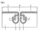
- Fig. 1 is a view showing a configuration of a distributed constant filter in accordance with a first embodiment of the present invention.
- this distributed constant filter includes an insulator substrate 1 formed of an insulator such as alumina ceramic, and a line pattern formed on insulator substrate 1.
- a ground layer, that is, a grounded electrode is formed on the entire back surface of insulator substrate 1.
- the line pattern includes lines 2 -9.
- Lines 2 and 3 are arranged with a prescribed interval on a straight line.
- Lines 2 and 3 are part of a micro-strip line and respectively form an input terminal and an output terminal of the filter.
- An electrical signal having a wavelength ⁇ is transmitted through the micro-strip line.
- Lines 4 and 5 are arranged parallel to each other in close proximity, and have their one end portions respectively connected to the end portions of lines 2 and 3.
- Lines 4 and 5 are arranged orthogonal to lines 2 and 3, respectively.
- Lines 4 and 5 form an electromagnetic field coupling portion 10.
- Lines 6 and 7 are both formed in L-shape and have their one end portions respectively connected to the other end portions of lines 4 and 5.
- the one sides of lines 6 and 7 are arranged parallel to lines 2 and 3, respectively, and the other sides are arranged in a direction orthogonal to lines 2 and 3, respectively.
- the distance from the open end of line 6, 7 to electromagnetic field coupling portion 10 is set to ⁇ /4.
- Lines 8 and 9 are both formed in U-shape and have their one sides arranged parallel to the other sides of lines 6 and 7, respectively, at a distance of about ⁇ /4 or less and their other sides arranged parallel at a distance of about ⁇ /4 or less.
- the other side of line 6 and the one side of line 8 form an electromagnetic field coupling portion 11; the other side of line 7 and the one side of line 9 form electromagnetic field coupling portion 12, and the other sides of lines 8 and 9 form an electromagnetic field coupling portion 13.
- Each of lines 8 and 9 forms a ⁇ /2 open line resonator.
- Figs. 2A and 2B are circuit diagrams showing equivalent circuits of the filter.
- Fig. 2A is a circuit diagram with great use of distributed constant line and
- Fig. 2B is a circuit diagram with only concentrated constant.
- the ⁇ /2 open line resonator formed of line 8 is equivalent to an LC parallel resonance circuit including a coil 8a and a capacitor 8b.
- Coil 8a has a prescribed inductance C1 and has its one electrode grounded.
- Capacitor 8b has a prescribed capacitance C1 and has its one electrode grounded. This is because, in the resonance frequency, the middle portion of line 8 is equivalently grounded and the impedance at the both ends becomes infinite.
- the ⁇ /2 open line resonator formed of line 9 is equivalent to an LC parallel resonance circuit including a coil 9a and a capacitor 9b.
- Coil 9a has a prescribed inductance L1 and has its one electrode grounded.
- Capacitor 9b has a capacitance C1 and has its one electrode grounded.
- Electromagnetic field coupling portion 11 is equivalent to a capacitor having a prescribed capacitance C2. This is because the open ends of lines 6 and 8 are arranged close to each other at a distance of about ⁇ /4 or less and in this case electromagnetic field coupling based on capacitive coupling occurs.
- electromagnetic field coupling portion 12 is equivalent to a capacitor having a prescribed capacitance C2.
- Electromagnetic field coupling portion 13 is equivalent to a capacitor having a prescribed capacitance C3.
- lines 4 and 5 are equivalent to two coils that have a prescribed inductance L2 and are coupled to each other with the coefficient of mutual induction K. This is because electromagnetic field coupling based on mutual inductive magnetic field coupling occurs when those parts of two lines 4 and 5 which are not the open ends are arranged parallel to each other in close proximity. Since this filter is designed such that the distance from the open end of line 6, 7 to electromagnetic field coupling portion 10 is set to ⁇ /4, the position of electromagnetic field coupling portion 10 is the current maximum point and the mutual inductive magnetic field coupling is readily created. Therefore the mutual inductive coupling is created efficiently in a limited space.
- the one electrodes of coil 8a and capacitor 8b of LC parallel resonance circuit 8 are grounded and the other electrodes of coil 8a and capacitor 8b are connected to an input terminal 2 through a capacitor 11 and a coil 4.
- the one electrodes of coil 9a and capacitor 9b of LC parallel resonance circuit 9 are grounded and the other electrodes of coil 9a and capacitor 9b are connected to an output terminal 3 through a capacitor 12 and a coil 5.
- the other electrodes of coil 8a and capacitor 8b are connected to the other electrodes of coil 9a and capacitor 9b through a capacitor 13. Coils 4 and 5 are brought into mutual inductive magnetic field coupling.
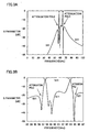
- Figs. 3A and 3B are graphs showing the frequency characteristics of the equivalent circuits shown in Figs. 2A and 2B.
- C1 0.8201pF
- C2 0.005445pF
- C3 0.06153pF
- L1 0.00786nH
- L2 1.257nH
- K 0.0319
- the center frequency is 60 GHz.
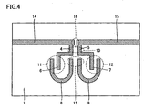
- this filter differs from the filter in Fig. 1 in that lines 2 and 3 are replaced with lines 14 and 15, respectively.
- Lines 14 and 15 are part of micro-strip line and respectively form an input terminal and an output terminal of the filter.
- Lines 14 and 15 are arranged on a straight line.
- the end portion of line 14 and the end portion of line 15 are arranged proximately at a distance of about ⁇ /4 or less and form an electromagnetic field coupling portion 16.
- Figs. 5A and 5B are circuit diagrams showing equivalent circuits of the filter shown in Fig. 4.
- Fig. 5A is a circuit diagram with great use of distributed constant line and
- Fig. 5B is a circuit diagram with only distributed constant.
- electromagnetic field coupling portion 16 is equivalent to a capacitor having a prescribed capacitance C4. This is because the open ends of lines 14 and 15 are arranged close to each other at a distance of about ⁇ /4 or less and in such coupling the electromagnetic field coupling based on capacitive coupling occurs. Therefore in this equivalent circuit, a capacitor 16 is connected between an input terminal 14 and an output terminal 15. The remaining configuration is same as the filter shown in Figs. land 2 and the description thereof will not be repeated.
- Figs. 6A and 6B are graphs showing the frequency characteristics of the equivalent circuit shown in Fig. 5B.
- C1 0.8811pF
- C2 0.005513pF
- C3 0.0595pF
- C4 0.002618pF
- L1 0.007506nH
- L2 1.255nH
- K 0.02913
- the center frequency is 60 GHz.
- a filter having the structure shown in Fig. 4 was actually prototyped and determined and the result is shown in Figs. 7A and 7B.
- This prototype filter was used as an RF filter of a radio communication circuit having a passband of 58 - 61 GHz and a local frequency of 57 GHz, and was designed specifically for suppressing an image frequency. Therefore two attenuation poles are certainly created at the frequencies above and below the passband, the lower frequency side of which are specially emphasized and designed.
- Fig. 7A shows the filter characteristics in the wider band and Fig. 7B is a graph with the enlarged filter characteristics in the vicinity of the passband.
- the total four attenuation poles are formed at the frequencies immediately above and below the passband so that the steepness at the lower frequency side is largely increased.
- the insertion loss of the passband is -4.0 to -2.6 dB
- the return loss of the passband is at least 17 dB
- the attenuation amount at the image frequency band of 53 - 56 GHz is at least 20.0 dB, resulting in practical performance.
- This prototype filter was formed by patterning on an alumina ceramic substrate having a thickness of 0.15 mm mainly with a copper material.
- a so-called line-and-space is 50 ⁇ m.
- the line width of the micro-strip line is 150 ⁇ m
- the line width for all lines including ⁇ /2 open line resonators 8 and 9 is 50 ⁇ m.
- Each length of ⁇ /2 open line resonators 8 and 9 is about 710 ⁇ m.
- the total distance branching from the micro-strip line having a line width of 150 ⁇ m to the open end of line 6, 7 is about 650 ⁇ m.
- the gap distance between feeder line 6, 7 and ⁇ /2 open line resonator 8, 9 is 50 ⁇ m
- the gap distance between two ⁇ /2 open line resonators 8 and 9 is 90 ⁇ m.
- the specific value of the size shown herein may vary easily with the substrate thickness, dielectric constant ⁇ of the substrate material, and the design rule of the line-and-space of the fine patterning, and therefore it is not absolute.
- a network analyzer and a wafer probe for millimeter waves were used. These measuring instruments were calibrated using an LRM calibration substrate and an LRM calibration program fabricated by the manufacture thereof. The wafer probe was fixed to a wafer probe station not to cause any change in a contact state such as a position shift during measurement.
- the number of ⁇ /2 open line resonators is not limited to two.
- the number of poles of resonance within the passband has to be increased and therefore the number of ⁇ /2 open line resonators has to be increased.
- the present invention may be applied to such a case.
- Fig. 8 is a view showing a configuration of a distributed constant filter in accordance with a third embodiment of the present invention. Referring to Fig. 8, this filter differs from the filter in Fig. 1 in that lines 8 and 9 are replaced with lines 21 - 23.
- Lines 21 and 22 are both formed in L-shape and have their one sides arranged in a direction orthogonal to lines 2 and 3, respectively, and their other sides arranged parallel to lines 2 and 3, respectively.
- the one side end portions of lines 22 and 23 are arranged parallel to the other side end portions of lines 6 and 7, respectively, at a distance of about ⁇ /4 or less.
- Line 23 is formed in U-shape and arranged between lines 21 and 22.
- the one side end portion of line 23 is arranged parallel to the one side end portion of line 21 at a distance of about ⁇ /4 or less.
- the other side end portion of line 23 is arranged parallel to the one side end portion of line 22 at a distance of about ⁇ /4 or less.
- the one side end portion of line 21 and the other side end portion of line 6 form an electromagnetic field coupling portion 24.
- the one side end portion of line 22 and the other side end portion of line 7 form an electromagnetic field coupling portion 25.
- the one side end portion of line 23 and the other side end portion of line 21 form an electromagnetic field coupling portion 26.
- the other side end portion of line 23 and the other side end portion of line 22 form an electromagnetic field coupling portion 27.
- Each of lines 21 - 23 forms a ⁇ /2 open line resonator.
- the ⁇ /2 open line resonator is not limited to have U-shape. Furthermore, in the present invention, the open end of the ⁇ /2 open line resonator does not necessarily involve the electromagnetic field coupling, and it may be isolated without the electromagnetic field coupling.
- Figs. 9A and 9B are circuit diagrams of equivalent circuits of the filter shown in Fig. 8.
- Fig. 9A is a circuit diagram with great use of distributed constant line and
- Fig. 9B is a circuit diagram with only concentrated constant.
- the ⁇ /2 open line resonator formed of line 21 is equivalent to an LC parallel resonance circuit including a coil 21a and a capacitor 21b.
- the ⁇ /2 open line resonator formed of line 22 is equivalent to an LC parallel resonance circuit including a coil 22a and a capacitor 22b.
- the ⁇ /2 open line resonator formed of line 23 is equivalent to an LC parallel resonance circuit including a coil 23a and a capacitor 23b.
- Coils 21a - 23a have the respective prescribed inductance L5 - L7 and have their respective one electrodes grounded.
- Capacitors 21b - 23b have the respective prescribed capacitance C5 - C7 and have their respective one electrode grounded.
- Electromagnetic field coupling portions 24 -27 are equivalent to capacitors having the respective prescribed capacitance C2, C2, C3, C3.
- the one electrodes of coil 21a and capacitor 21b of LC parallel resonance circuit 21 are grounded, and the other electrodes of coil 21a and capacitor 21b are connected to input terminal 2 through a capacitor 24 and coil 4.
- the one electrodes of coil 22a and capacitor 22b of LC resonance circuit 22 are grounded, and the other electrodes of coil 22a and capacitor 22b are connected to output terminal 3 through a capacitor 25 and coil 5.
- the one electrodes of coil 23a and capacitor 23b of LC parallel resonance circuit 23 are grounded and the other electrodes of coil 23a and capacitor 23b are connected to a node between capacitor 24 and LC parallel resonance circuit 21 through capacitor 26 and also connected to a node between capacitor 25 and LC parallel resonance circuit 22 through capacitor 27.
- Coils 4 and 5 are brought into mutual inductive magnetic field coupling.
- three ⁇ /2 open line resonators 21 -23 are provided so that a filter with a band wider than that in the first and second embodiments can be created.
- Figs. 10A - 10C are view showing a configuration of a filter in accordance with a fourth embodiment of the present invention.
- This filter includes an insulator substrate 30 and a line pattern formed on opposite surfaces thereof.
- Fig. 10A is a perspective view on the whole
- Fig. 10B shows the pattern on the front surface of the substrate
- Fig. 10C shows the pattern on the back surface of the substrate.
- This filter is not a filter provided for a micro-strip line but a filter provided for a coplanar line.
- a line 31 corresponding to lines 2, 4 and 6 in Figs. 2A and 2B provided on the front surface of substrate 30 are a line 31 corresponding to lines 2, 4 and 6 in Figs. 2A and 2B, a line 32 in L-shape, and a ground layer 33 formed to surround lines 31 and 32.
- the tip portion of line 31 and the one end portion of line 32 are arranged parallel in proximity.
- the other end portion of line 32 is connected to ground layer 33.
- a line 34 corresponding to lines 3, 5 and 7 in Figs. 2A and 2B, a line 35 in L-shape, and a ground layer 36 formed to surround lines 34 and 35.
- the tip portion of line 34 and the one end portion of line 35 are arranged parallel in proximity.
- the other end portion of line 35 is connected to ground layer 36.
- Fig. 10A those parts of lines 31 and 34 which correspond to lines 4 and 5 in Fig. 1 are arranged in such a manner that they are overlapped above and below, to form an electromagnetic field coupling portion 37.
- the tip portions of lines 31 and 34 and the one end portions of lines 32 and 35 form electromagnetic field coupling portions 38 and 39, respectively.
- the one end portion of line 32 and the one end portion of line 35 form an electromagnetic field coupling portion 40.
- Each of lines 38 and 39 forms a ⁇ /4 short-circuited line resonator.
- the equivalent circuits of this filter are same as the equivalent circuits in Figs. 2A and 2B.
- the ⁇ /4 short-circuited line resonators 32 and 35 form LC parallel resonance circuits 8 and 9, respectively.
- Electromagnetic field coupling portions 38, 39 and 40 form capacitors 11, 12 and 13, respectively.
- Electromagnetic field coupling portion 37 forms coils 4 and 5 in mutual inductive magnetic filed coupling.
- the coupling between front and back patterns of monolayer substrate 30 was used to obtain a strong mutual inductive magnetic field coupling.
- the interlayer coupling with upper and lower patterns on different layers in two or more multi-layer substrate may be used other than this method.
- Figs. 11A and 11B are views showing a configuration of a filter in accordance with a fifth embodiment of the present invention. This filter is implemented with the circuit diagram in Fig. 2 in a form suitable for the semi-microwave band.
- Fig. 11A is a perspective view of the filter
- Fig. 11B is a plan view of the filter seen from above.
- this filter is formed of an insulator substrate 41 and a plurality of discrete components.
- a ground electrode 42 is formed on the entire back surface of substrate 41 and electrodes 43 - 49 are formed on the front surface of substrate 41.
- Electrode 43 is connected to ground electrode 42 through a plurality of via holes 50.
- LC parallel resonance circuits 8 and 9 in Figs. 2A and 2B are implemented by so-called dielectric resonators 51 and 52.
- Dielectric resonator 51, 52 is a known technique that has already been utilized in the semi-microwave band, and has a coaxial structure in which an insulator such as alumina ceramic is sandwiched between an outer conductor and a center conductor.
- the length of dielectric resonator 51, 52 is designed to the length of ⁇ /4 relative to the wavelength ⁇ around the center frequency of the filter, each of one ends 51a and 51b is connected to electrode 43 with the outer conductor and the center conductor being short-circuited and each of the other ends 51b and 52b is open-ended.
- the center conductors of resonators 51 and 52 are connected to electrodes 44 and 45 on substrate 41 through lead pins 51c and 52c, respectively.
- Capacitors 11 -13 in Figs. 2A and 2B are implemented by chip capacitors 53 - 55, respectively, in the fifth embodiment. Chip capacitors 53 - 55 are connected respectively between electrodes 44 and 46, 45 and 47, 44 and 45. Furthermore, electromagnetic field coupling portion 10 in Figs. 2A and 2B is implemented by a transformer 56 as a discrete component in this filter. Transformer 56 includes terminals 56c - 56f, a coil 56a connected between terminals 56c and 56d, and a coil 56b connected between terminals 56e and 56f as shown in Fig. 12. Coils 56a and 56b are brought into the mutual inductive magnetic field coupling. Terminals 56c - 56f are respectively connected to electrodes 48, 46, 49, and 47. Electrodes 48 and 49 form input terminal 2 and output terminal 3.
- the present invention is not limited to the distributed constant circuit for the millimeter wave band and can be implemented with a circuit with a lower frequency using a discrete component.
- the present invention can easily be applied not only to one dual-terminal filter circuit but to a triple-terminal duplexer-type filter circuit or a multiplexer type filter circuit having three or more terminals.
- the millimeter wave in the 60 GHz band is used as indoor radio transmission wave.
- the millimeter wave in the 60 GHz band has a frequency significantly higher than the present satellite TV broadcast wave and provides a wide radio bandwidth for a transceiver, so that ground broadcast and satellite broadcast can collectively be transmitted wirelessly.
- this frequency band the absorption by oxygen and moisture is great and therefore the blocking between adjacent houses is easy.
- 1/2 wavelength is 2.5 mm in the air, which is equivalent to the chip size of IC, so that the antenna can be integrated with IC. This reduces the equipment in size, and light and small radio modules can be built into electronic equipment. Therefore this frequency band is suitable for indoor radio transmission at home.
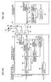
- Figs. 13, 14A and 14B are block diagrams showing the configuration of the high frequency radio communication device in accordance with the sixth embodiment of the present invention.
- this high frequency radio communication device includes a millimeter wave transmitting device 60, a millimeter wave receiving device 76, and electronic equipment 89.
- Millimeter wave transmitting device 60 includes a VHF/UHF antenna 61, a BS antenna 62, a CS antenna 63, a connector 64, a connector 65, a broadcast wave input unit 66, a frequency arrangement unit 67, an up-converter 68, a bandpass filter (BPF) 68a, a transmission unit 69, a power supply unit 70, a power supply unit 71, a reception unit 72, a power supply control unit 73, an available device storage unit 74, and a millimeter wave transmitting antenna 75.
- BPF bandpass filter
- Millimeter wave receiving device 76 includes a millimeter wave receiving antenna 77, an amplifying unit 78, a bandpass filter 78a, a down-converter 79, a reverse frequency arrangement unit 80, a mixing/switching unit 81, a power supply control unit 82, a power receiving unit 83, a control signal receiving unit 84, transmission unit 85, an antenna terminal 86, an antenna terminal 87, and a connector 88.
- Electronic equipment 89 includes an antenna terminal 90, a broadcast signal receiving unit 91, a control signal transmitting unit 92, a power supply unit 93, and a memory unit 94.
- electronic equipment 89 is for example a TV receiver, a display unit or the like is provided other than the configuration described above, although not shown in Figs. 14A and 14B.
- millimeter wave transmitting unit 60 and millimeter wave receiving unit 76 First, that part which is related to the basic millimeter wave transmission in millimeter wave transmitting unit 60 and millimeter wave receiving unit 76 will be described.
- Radio waves from ground broadcast or satellite broadcast are input to connectors 64 and 65 through VHF/UHF antenna 61, BS antenna 62 or CS antenna 63.
- two connectors 64 and 65 are shown here, the present invention is not limited thereto and any number of connectors can be provided depending on the connection situation.
- antennas are connected here, a supply terminal for collective broadcast waves from a community receiving system such as CATV may be connected.
- the broadcast wave input from connectors 64 and 65 is supplied to broadcast wave input unit 66.
- Broadcast wave input unit 66 is usually formed of an amplifier having its gain set appropriately depending on the frequency band, the modulation format and the like, and the amplified broadcast wave is supplied to frequency arrangement unit 67.
- Frequency arrangement unit 67 includes amplifiers 111 and 112, filters 113 and 114, a frequency mixer 115, and a local oscillator 116, as shown in Fig. 15.
- Amplifier 111 amplifies BS and CS broadcast signals.
- Filter 113 removes unnecessary frequency components from the output signal from amplifier 111.
- Amplifier 112 amplifies a ground wave broadcast signal
- Frequency mixer 115 and local oscillator 116 convert the frequency of the output signal from amplifier 112.
- Filter 114 removes unnecessary signal components from the frequency-converted signal.
- the CS and BS intermediate frequency in the signal input to frequency arrangement unit 67 is arranged on a frequency axis of intermediate frequency 1035 MHz - 1895 MHz, as shown in Fig. 17A, by a block converter (not shown) provided between connector 65 and CS antenna 63 in a case of the community reception.
- Only the ground wave broadcast signal of such input signal is converted in frequency by frequency mixer 115 and local oscillator 116 in frequency arrangement unit 67 and is arranged on the side of the frequency higher than CS broadcast signal on the frequency axis, as shown in Fig. 17B. Since the frequency of the ground wave broadcast is lower, the signal that is up-converted to the 60 GHz band comes into the vicinity of the local oscillating wave.
- This local oscillating wave is essentially an unnecessary wave that has to be removed without being radiated from the antenna. Therefore if the ground wave broadcast is up-converted as it is, it is removed along with the local oscillating wave. Consequently, the ground broadcast wave is converted in frequency to the other frequency band (for example 2 GHz band) at the intermediate frequency stage in frequency arrangement unit 67.
- the other frequency band for example 2 GHz band
- the broadcast wave arranged on the frequency axis in this way is up-converted to the 60 GHz band by up-converter 68 within millimeter wave transmitting device 60 with the unnecessary wave being removed by bandpass filter 68a, resulting in the radio frequency as shown in Fig. 17C, which is amplified in power in transmission unit 69 and is output as a millimeter wave radio signal from millimeter wave transmitting antenna 75 of millimeter wave transmitting device 60.
- the millimeter wave radio signal received at millimeter receiving antenna 77 of millimeter wave receiving device 76 is amplified by amplifying unit 78 with the image signal being removed by bandpass filter 78a, is thereafter down-converted by down-converter 79, and is input to reverse frequency arrangement unit 80.
- Bandpass filters 68a and 78a are formed of the filters described in the first to fifth embodiments.
- Reverse frequency arrangement unit 80 includes amplifiers 121 and 122, filters 123 and 124, frequency mixer 125, and local oscillator 126, as shown in Fig. 16.
- Amplifier 121 amplifies the reproduced BS and CS broadcast signals.
- Filter 123 removes unnecessary frequency components from the output signal from amplifier 121.
- Amplifier 124 amplifies the reproduced ground wave broadcast signal.
- Filter 124 removes unnecessary frequency components from the output signal of amplifier 122.
- Frequency mixer 125 and local oscillator 126 converts the frequency of the signal that is passed through filter 124.
- Reverse frequency arrangement unit 80 has a function of converting the frequency from the intermediate frequency on the frequency axis to the original ground wave frequency using frequency mixer 125 and local oscillator 126 through a process that is the reverse of frequency arrangement unit 67.
- the resulting broadcast wave is input to electronic equipment 89, which is in turn ready for TV reception if it is a TV receiver.
- the foregoing is the basic configuration for transmitting in millimeter waves the broadcast waves collectively to electronic equipment 89 such as a TV receiver through millimeter wave transmitting unit 60 and millimeter wave receiving device 76.
- Electronic equipment 89 such as a TV receiver uses broadcast signal receiving unit 91 to select and receive the broadcast wave supplied from antenna terminal 90.
- VHF/UHF antenna 61, BS antenna 62 or CS antenna 63 is directly connected to antenna terminal 90.
- antenna terminal 90 is connected to connector 88.
- Millimeter wave receiving device 76 is provided with mixing/switching unit 81 and antenna terminals 86 and 87. Therefore when millimeter wave receiving device 76 is attached to electronic equipment 89, VHF/UHF antenna 61, BS antenna 62 or CS antenna 63 is also connected directly to antenna 86 or 87 to allow the broadcast waves therefrom to be used through mixing/switching unit 81. When millimeter wave receiving device 76 is used, antenna terminals 86 and 87 usually need not be connected.
- VHF/UHF antenna 61, BS antenna 62, CS antenna 63 and the like can be connected without any change to the connection where millimeter wave receiving device 76 is connected to electronic equipment 89.
- the user When the user selects the desired channel to receive using broadcast signal receiving unit 91 in electronic equipment 89, the user stores beforehand whether the received channels are the direct inputs from VHF/UHF antenna 61, BS antenna 62, CS antenna 63 and the like, or the inputs through millimeter wave transmitting device 60 and millimeter wave receiving device 76 in association with the received channels, in memory unit 94. Based on the information stored in memory unit 94, if the selected received channel is the one to use millimeter wave transmitting device 60 and millimeter wave receiving device 76, the power supply necessary for the operation of millimeter wave receiving device 76 is fed by power supply unit 93 through antenna terminal 95. The power is supplied with the broadcast wave superposed thereon.
- the power may be supplied by power supply unit 93 when electronic equipment 89 is turned on, and the power supply control of power supply control unit 82 may be performed as necessary with the superposed control signal from control signal transmitting unit 92.
- the power supply and the control signal passed through connector 88 are supplied through power receiving unit 83 and control signal receiving unit 84 to power supply control unit 82 respectively separate from the broadcast wave.
- the power consumption is suitably reduced if the power is supplied from power supply unit 93 when electronic equipment 89 requires a reception operation.
- power supply control unit 82 controls the power supply to amplifying unit 78, down-converter 79 and reverse frequency arrangement unit 80, it may control the other block that requires the power supply control.
- millimeter wave receiving device 76 in addition to electronic equipment 89 may be used or millimeter wave receiving device 76 itself may include a power supply circuit that receives power supply from AC power supply, as electronic equipment 89 does not always support power supply to millimeter wave receiving device 76.
- control signal transmitting unit 92 can transmit information that specifies vertically polarized waves or horizontally polarized waves to be used depending on the received channel to CS antenna 63, in addition to the control of the power supply.
- BS broadcast reception it transmits information about whether power is supplied to BS antenna 62.
- the information about vertically polarized waves or horizontally polarized waves, or BS reception and the like is created by control signal receiving unit 92, is transmitted through antenna terminal 90 and connector 88, and is separated by control signal receiving unit 84.
- the separated information is transmitted by transmission unit 85 to millimeter wave transmitting unit 60.
- signal is usually transmitted from transmission unit 85 to reception unit 72 using infrared radiation, the present invention is not limited to infrared and may use radio wave, wire, voice, power-line carrier and the like.
- the radio waves in UHF band can transmit through shields such as screens and walls, unlike infrared communication, to allow the millimeter wave transmitting device and the millimeter wave receiving device to be used for divided rooms.
- a cordless phone such as a PHS
- data transmission can be realized, in addition to a signal for horizontal and vertical polarization control, to allow for two-way communications.
- the power supply is cut off to a circuit block that needs not operate, including amplifying unit 78, down-converter 79, reverse frequency arrangement unit 80 and the like in millimeter wave receiving device 76, and the power supply has to be controlled to a circuit block that needs not operate, including broadcast wave input unit 66, frequency arrangement unit 67, up-converter 68, transmission unit 69 and the like in the millimeter wave transmitting device 60.
- a transmission output from one millimeter wave transmitting device 60 is provided to a combination of a plurality of millimeter wave receiving devices 76 and electronic equipment 89, for example, where electronic equipment 89 is a large stationary TV receiver and a portable liquid crystal TV receiver which are provided with the respective millimeter wave receiving devices 76. Therefore in this case electronic equipment 89 as a large stationary TV receiver and electronic equipment 89 as a portable liquid crystal TV receiver respectively transmit equipment identification information and information indicating that that equipment now requires reception, for example, information indicative of ON to millimeter wave receiving devices 76 that are respectively connected thereto, using control signal transmitting unit 92. The transmitted information is separated by control signal receiving unit 84 and transmitted to one millimeter wave transmitting device 60 by transmission unit 85.
- Millimeter wave transmitting device 60 receives this information at reception unit 72 and transmits it to available equipment storing unit 74.
- Available equipment storing unit 74 allows the user to store the equipment that uses the broadcast wave of millimeter wave transmitting device 60 in advance, and obtains the equipment identification information and the information indicating that that equipment now requires reception for pieces of equipment stored therein from reception unit 72. If all pieces of equipment stored in available equipment storing unit 74 are turned off and do not require the broadcast waves, power supply control unit 73 then cuts off the power supply to broadcast wave input unit 66, frequency arrangement unit 67, up-converter 68, transmission unit 69, and the like, and also power supply units 70 and 71 cuts off the power supply to CS antenna 63, BS antenna 62 and the like. In this way, the power consumption can be reduced when millimeter wave transmitting device 60 and millimeter wave receiving device 76 are not required.
- a filter excellent in steepness can be realized with a low-cost planar print circuit.
- the steepness is not high simply because of a narrow band filter.
- the steepness can be increased while for example 5 % or more in the specific bandwidth can be ensured.
- the filter in accordance with the present invention may be used as an RF filter to remove local signals and image signals so that the device can advantageously be miniaturized, simplified and reduced in cost.
- a communication circuit for extremely high frequency such as millimeter wave band
- a waveguide type filter or a filter having such a structure in that a charger resonator is enclosed in a metal case has been used as a filter circuit.
- a balance type MMIC mixer has been used to provide a mixer with a filter function.
- all of these techniques have problems in size or cost.
- the device as a whole can be miniaturized in a casing structure and the like, be simplified, and be reduced in cost.
- the filter circuit in accordance with the present invention is effective particularly when it is used in a wideband radio system in the millimeter wave band. Furthermore, the filter circuit of the present invention is effectively employed to reduce the cost and size in the wideband system in the millimeter wave band as disclosed in Japanese Patent Laying-Open No. 2000-353971.
Landscapes
- Physics & Mathematics (AREA)
- Electromagnetism (AREA)
- Control Of Motors That Do Not Use Commutators (AREA)
- Input Circuits Of Receivers And Coupling Of Receivers And Audio Equipment (AREA)
Abstract
In a distributed constant filter, two λ/2 open line resonator (8, 9) are
capacitive-coupled by an electromagnetic field coupling portion (13), and an
input terminal (2) and an output terminal (3) are brought into mutual
inductive coupling by an electromagnetic field coupling portion (10). The
frequency of an attenuation pole can be close to a center frequency and the
steepness of the filter characteristics can be increased.
Description
The present invention relates to a filter circuit and a high frequency
communication circuit device using the same, and more particularly to a
filter circuit selectively passing a predetermined frequency component of a
signal input to an input terminal to an output terminal and a high
frequency communication circuit device using the same.
In the low frequency band, most of filter circuits are fabricated by
attaching discrete components such as coils or capacitors. In the high
frequency band such as microwave or millimeter wave bands, however,
they are usually fabricated with distributed constant type circuits.
Fig. 18 is a perspective view showing a configuration of an edge
coupled filter as a representative distributed constant filter. This filter is
provided for a micro-strip line that is most common as a distributed
constant line. In Fig. 18, this filter includes a substrate 150 formed of an
insulator such as alumina ceramic. A ground layer 151 is formed on the
entire back surface of substrate 150. Lines 152 and 153 are part of the
micro-strip line as a high frequency transmission line and respectively form
an input terminal and an output terminal for the filter. Lines 154 and 155
form so-called λ/2 open line resonators. As used herein λ is a wavelength
of the electrical signal transmitted through the line, in the frequency in the
vicinity of the center frequency of the filter circuit. Generally, micro-strip
lines 152 and 153 and λ/2 open line resonators 154 and 155 are collectively
patterned with high accuracy on the surface of insulator substrate 150 by
means of print or photolithography. Therefore the planar circuit filter
having the structure in Fig. 18 is generally known as a filter circuit with
low cost and with excellent productivity.
In the following, a distributed constant type filter circuit formed of
micro-strip lines as shown in Fig. 18 will mainly be described in the present
specification. The effect of the present invention, however, is not limited
to such a filter. It can readily be applied to a filter circuit formed of a
coplanar line or a semi-concentrated constant type filter with a part of
circuit elements replaced with concentrated constant discrete components.
Furthermore, in the following, only a planar view of a substrate seen from
above will be shown as a view showing the structure of the distributed
constant filter, for the sake of brevity, in the present specification.
Equivalent circuits having the structure of Fig. 18 are shown in Figs.
19A and 19B. In the following, in the present specification, the equivalent
circuit is shown in two stages to facilitate understanding. First, Fig. 19A
is an equivalent circuit that is represented with great use of distributed
constant line in a one-to-one correspondence with the structure of Fig. 18.
However, the equivalent circuit including a distributed constant line as
shown in Fig. 19A is inconvenient in a later simulation. Assuming that
calculation is made using a commercially available high frequency circuit
simulator, the calculation results somewhat vary depending products and
manufactures and methods of defining parameters are so varied to
understand. In the present specification, an equivalent circuit with only
concentrated constant in Fig. 19B is illustrated together, and the
simulation is mainly performed using the equivalent circuit with only
concentrated constant. The two types of equivalent circuits in Figs. 19A
and 19B are equivalent in the vicinity of resonance frequency of the filter.
This is because a λ/2 open line resonator is equivalent to an LC parallel
resonance circuit having one end grounded in the vicinity of its resonance
frequency.
In Figs. 19A and 19B, an LC parallel resonance circuit 154 including
a coil 154a and a capacitor 154B having one end grounded and an LC
parallel resonance circuit 155 including a coil 155a and a capacitor 155b
having one end grounded correspond to λ/2 open line resonators 154 and
155 in Fig. 18, respectively. Each of coils 154a and 155b has a prescribed
inductance L1 and each of capacitors 154b and 155b has a prescribed
capacitance C1. This is because, in the resonance frequency, the middle
portion of the λ/2 open line resonator is equivalently grounded and the
impedance is close to infinity at both open ends. Capacitors 156 and 157
having a capacitance C2 in Figs. 19A and 19B correspond to
electromagnetic field coupling portions 156 and 157 in Fig. 18. In
electromagnetic field coupling portions 156 and 157, micro-strip lines 152
and 153 and λ/2 open line resonators 154 and 155 are arranged closely
spaced apart from each other at the open ends approximately by λ/4 or less.
In such a case, it is known that electromagnetic field coupling occurs based
on capacitive coupling. Capacitor 158 having a capacitance C3 in Figs.
19A and 19B corresponds to an electromagnetic field coupling portion 158
in Fig. 18. In electromagnetic field coupling portion 158, lines 154 and 155
are arranged close to each other at the open ends. In this case, it is known
that electromagnetic field coupling occurs based on capacitive coupling.
The present invention aims at a filter circuit for use in extremely
high frequency band such as millimeter wave band, in particular. An
exemplary equivalent circuit in Fig. 19B that is optimally designed for 60
GHz band is shown. Figs. 20A and 20B are frequency characteristics
graphs of that filter. The passband is designed as 58 - 61 GHz consistently
in the present specification. Assume C1 = 0.3661pF, C2 = 0.0527pF, C3 =
0.02884pF, L1 = 0.01699nH. In Figs. 20A and 20B, the axis of abscissas
represents the frequency [GHz] and the axis of ordinates represent the
absolute value of S parameters expressed in dB. In Figs. 20A and 20B,
S21 representing the pass characteristics and S11 representing the
reflection characteristics are plotted at the same time. Fig. 20A shows the
characteristics of the wide band and Fig. 20B shows the characteristics of
the vicinity of the passband. As can be seen from Figs. 20A and 20B, the
filter having the structure in Fig. 18 functions as a bandpass filter.
In the following, the graphs in the formats shown in Figs. 20A and
20B will be used to express the filter characteristics. Furthermore, in the
present specification, the operation principle of the filter will be described,
as shown in Figs. 18 - 20B, by first showing the structure, then showing the
equivalent circuit thereof, and finally showing the calculation result of the
filter characteristics of the equivalent circuit. It is noted that in a second
embodiment of the present invention, the effectiveness of the present
invention is validated by showing the measurement result of the filter that
was actually prototyped rather than only by calculation results.
Bandpass filters with high steepness are in the greatest demand
among the filters. For local filters or image filters for the extremely high
frequency band such as the millimeter wave band, filters with high
steepness are essential, as the passband is in the close vicinity of the
attenuation band. On the contrary, for example the filter of Fig. 18 results
in the filter characteristics that are gradual with poor steepness as shown
in Figs. 20A and 20B, without some special scheme. Then, in order to
improve the steepness of such a bandpass filter, the design method of
creating attenuation poles at the frequencies immediately above and below
the passband has been developed.
Some specific structures of such a filter having attenuation poles at
the frequencies above and below the passband have already been presented
in the academy. Among others, for example, a circuit shown in Fig. 21 has
been known as a circuit that achieves satisfactory results in the extremely
high frequency band such as the millimeter wave band and has a simple
structure for facilitating design ("Low Loss Micromachined Filters For
Millimeter-Wave Telecommunication Systems", Pierre Blondy et al., 1998
IEEE MTT-S Digest, pp. 1181-1184).
In Fig. 21, this filter includes an insulator substrate 161 formed of
alumina ceramic or the like, micro-strip lines 162 and 163 formed on the
surface thereof, and λ/2 open line resonators 164 and 165. Portions 167 -
170 enclosed by dotted lines are portions where lines 162 - 165 are close to
each other to cause electromagnetic field coupling. It is noted that
attention has to be made to the following two points in referring to the
aforementioned reference (MTT-S Digest). First, the aforementioned
reference assumes that it is characterized in that low loss can be attained
by the micromachine technique. However, this is not essential in the
operation principle of the filter, and the operation principle itself is same as
the filter in Fig. 21. Second, the aforementioned reference describes both
of a filter (two-pole filter) having two λ/2 open line resonators and a filter
(four-pole filter) having four λ/2 open line resonators. The effect of the
invention will be discussed in vain unless the filters are compared under
the same conditions. The discussion in the present specification is
consistently based on the filter (two-pole filter) having two λ/2 open line
resonators, for the sake of brevity.
Figs. 22A and 22B are circuit diagrams showing the equivalent
circuit of the filter in Fig. 21. Fig. 22A is an equivalent circuit with great
use of distributed constant line and Fig. 22B is an equivalent circuit
represented with only distributed constant. In Figs. 22A and 22B, an LC
parallel resonance circuit 164 including a coil 164a and a capacitor 164b
having one end grounded and an LC parallel resonance circuit 165
including a coil 165a and a capacitor 165b having one end grounded
correspond to λ/2 open line resonators 164 and 165 in Fig. 21, respectively.
Each of coils 164a and 165a has a prescribed inductance L1 and each of
capacitors 164b and 165b has a prescribed capacitance C1. Capacitors 168
and 169 having a capacitance C2 in Figs. 22A and 22B correspond to
electromagnetic field coupling portions 168 and 169 in Fig. 21, respectively.
A capacitor 167 having a capacitance C3 in Figs. 22A and 22B corresponds
to an electromagnetic field coupling portion 167 in Fig. 21. The coefficient
of mutual induction coupling K of Figs. 22A and 22B corresponds to an
electromagnetic field coupling portion 170 in Fig. 21. In electromagnetic
field coupling portion 170, the middle portions of two λ/2 open line
resonators 164 and 165, that is, the portions where the current is maximum
are arranged to align closely parallel to each other. In this case, it is
known that electromagnetic field coupling based on mutual inductive
magnetic field coupling occurs.
An exemplary equivalent circuit in Fig. 22B that is optimally
designed for 60 GHz band is shown. Figs. 23A and 23B are graphs
showing the frequency characteristics of that filter. Assume that C1 =
0.3546pF, C2 = 0.05981pF, C3 = 0.00687pF, L1 = 0.01846nH, K = 0.0914.
As can be seen from Fig. 23A, the following changes take place as compared
with Fig. 20A. Attenuation poles are formed at the frequencies above and
below the passband, and the steepness of the filter is increased in the
vicinity of these attenuation poles. At the attenuation pole on the lower
frequency side (48 GHz), S21 in Fig. 20A is -30 dB whereas S21 in Fig. 23A
is -50 dB or below. At the attenuation pole on the higher frequency side
(69 GHz), S21 in Fig. 20A is -17 dB whereas S21 in Fig. 23A is -50dB or
below. In other words, in a case of a radio communication device in which
a local frequency happens to be positioned at 48 GHz relative to the center
frequency of 60 GHz, the filter characteristics in Figs. 23A and 23B are
more advantageous than the filter characteristics of Figs. 20A and 20B, as
it provides more attenuation amount.
The filter of the equivalent circuit in Fig. 22A, 22B is a commonly
known circuit configuration and is described in many references. For
example, it is described in the second chapter of "Design and Application of
Communication Filter Circuit" (edited and authored by Yoshihiro Konishi,
Sogo Denshi Shuppan), which is a prominent text book of the high
frequency filter technique.
The conventional filter, however, has the problem in that the
steepness of the filter is not sufficient when it is used in a radio
communication device for the extremely high frequency band such as the
millimeter wave band, in particular. As the frequencies at two
attenuation poles are closer to the frequency of the passband (for example
59 - 62 GHz), the steepness of the filter characteristics becomes high. In
the case of the filters in Figs. 19A and 19B, however, the steepness of the
graph in Figs. 23A and 23B approaches its limit, which can be confirmed
easily with a common circuit simulation. Although the specific values
vary depending on minute condition settings such as specific bandwidth or
attenuation amount, for the filter characteristics of Figs. 23A and 23B, for
example, the frequencies at the attenuation poles can be set only at the
frequencies as far as 15 % or more apart when represented as being
standardized by the center frequency. If the attenuation poles are forced
to be closer, the waveform of the filter characteristics is distorted.
In an attempt to use a filter for attenuating a local signal, the
conventional filter having the characteristics of Figs. 23A and 23B is
sufficient as long as the local frequency is positioned at 48 GHz relative to
the center frequency 60 GHz. In most of the actual millimeter wave radio
communication device, however, the local frequency is often positioned at
the frequency closer to the center frequency 60 GHz, for example 57 GHz or
58 GHz. In such a case, with the conventional filter, the steepness is not
sufficient and the attenuation amount cannot be assured.
It is noted that in the discussion of this problem the steepness of the
filter varies depending on the minute condition settings such as specific
bandwidth or attenuation amount. For example, referring to the
characteristics (Fig. 3) of the filter (two-pole filter) under the same
conditions as those described in the aforementioned reference (MTT-S
Digest), the frequencies at the attenuation poles successively come to close
at more than 8 % when represented as being standardized by the center
frequency. The main reason for this, however, is simple: the filter
contemplated in the aforementioned reference is for a band quite narrower
than the filter contemplated in the present specification (specific bandwidth
= 3.5 %). The steepness of the filter is easier to understand in its effect in
the discussion of the somewhat wider band. Therefore all the filters with
the graphs in the present specification are unified with the specific
bandwidth of more than 5 %. Furthermore, the comparison of the filter
performance has difficulty in that an accurate comparison cannot be made
unless a variety of conditions are unified. For these reasons, in the
present specification, the filters are evaluated based on the simulation
results of the equivalent circuits for the purpose of unifying the conditions.
In addition, an optimum design function of a common, commercially
available circuit simulation program was used since an accurate
comparison is difficult with a manual design in determining the circuit
constant of the equivalent circuit.
The present invention is made to solve the problems described above
and the object is to provide a filter circuit having steep filter characteristics.
In accordance with the present invention, a filter circuit includes: a
plurality of resonators wherein an impedance between respective
input/output terminals and a reference potential line is maximum in each
resonance frequency and each input/output terminal is capacitive-coupled
to at least one of other input/output terminals; first capacitive coupling
means for capacitive-coupling input/output terminals of any two resonators
of the plurality of resonators and first and second terminals respectively to
each other; and electromagnetic field coupling means for connecting the
first and second terminals respectively to the input terminal and the output
terminal and bringing the input terminal and the output terminal into
magnetic field coupling by mutual induction. Therefore the frequency at
an attenuation pole can be close to a center frequency without degrading
the waveform of the filter characteristics and the steepness of the filter
characteristics can be increased.
Preferably, second capacitive coupling means for capacitive-coupling
the input terminal and the output terminal to each other is further
included. In this case, the number of attenuation poles can be increased
and an attenuation amount of the cut-off band can be increased.
Preferably, the filter circuit is formed of a line pattern made of a
conductor formed on an insulator substrate. Each of the plurality of
resonators includes a first line having a predetermined line length. At
least one end portion of both end portions of each first line is capacitive-coupled
to one end portion of another first line. The first capacitive
coupling means includes third and fourth lines having respective one end
portions capacitive-coupled to the other end portions of two first lines
included in the two resonators and having respective other end portions
connected to the first and second terminals. The electromagnetic field
coupling means includes fifth and sixth lines connected between the first
and second terminals and the input terminal and the output terminal,
respectively, each having at least a part arranged parallel to the other in
proximity. In this case, the filter circuit can be realized with a planar
print circuit thereby allowing for reduction in size and cost of the circuit.
Preferably, in accordance with another aspect of the present
invention, a filter circuit includes: a plurality of resonators wherein an
impedance between respective input/output terminals and a reference
potential line is maximum in each resonance frequency and each
input/output terminal is capacitive-coupled to at least one of other
input/output terminals; first capacitive coupling means for capacitive-coupling
input/output terminals of any two resonators of the plurality of
resonators and first and second terminals respectively to each other;
electromagnetic field coupling means for connecting the first and second
terminals respectively to the input terminal and the output terminal and
bringing the input terminal and the output terminal into magnetic field
coupling by mutual induction; and second capacitive coupling means for
capacitive-coupling the input terminal and the output terminal to each
other. Each of the plurality of resonators includes a first line having a
predetermined line length. At least one end portion of both end portions of
each first line is capacitive-coupled to one end portion of another first line.
The first capacitive coupling means includes third and fourth lines having
respective one end portions capacitive-coupled to the other end portions of
two first lines included in the two resonators and having respective other
end portions connected to the first and second terminals. The
electromagnetic field coupling means includes fifth and sixth lines having
respective one end portions respectively connected to the first and second
terminals, each having at least a part arranged parallel to the other in
proximity. The second capacitive coupling means includes seventh and
eighth lines connected between the other end portions of the fifth and sixth
lines and the input terminal and the output terminal, respectively, and
each having at least a part arranged proximate to the other. Therefore the
frequency at the attenuation pole can be close to the center frequency
without degrading the waveform of the filter characteristics and the
steepness of the filter characteristics can be increased. Moreover, the filter
circuit can be realized with a planar print circuit thereby allowing for
reduction in size and cost of the circuit.
Preferably, the fifth and sixth lines are proximate to each other at a
position of a quarter wave of a signal having a center frequency of the filter
circuit from open ends of the third and fourth lines. In this case, since the
current value is maximum in the fifth and sixth lines, the mutual inductive
magnetic field coupling between the fifth and sixth lines can be created in a
limited space efficiently.
Preferably, each of the plurality of resonators is a quarter wave
short-circuited line resonator or a half wave open line resonator. In this
case, the filter circuit can be realized with a planar print circuit thereby
allowing for reduction in size and cost of the circuit.
In accordance with the present invention, the filter circuit is used as
a part of a multiplexer type filter circuit. In this case, the multiplexer
circuit can be improved in performance and reduced in cost and size.
In a high frequency communication circuit device in accordance with
the present invention, the filter circuit described above is used as a high
frequency circuit for removing a local signal or an image signal. In this
case, a high frequency communication circuit device can be improved in
performance and reduced in cost and size.
Fig. 1 is a view showing a configuration of a distributed constant
filter in accordance with a first embodiment of the present invention. In
Fig. 1, this distributed constant filter includes an insulator substrate 1
formed of an insulator such as alumina ceramic, and a line pattern formed
on insulator substrate 1. A ground layer, that is, a grounded electrode is
formed on the entire back surface of insulator substrate 1.
The line pattern includes lines 2 -9. Lines 2 and 3 are arranged
with a prescribed interval on a straight line. Lines 2 and 3 are part of a
micro-strip line and respectively form an input terminal and an output
terminal of the filter. An electrical signal having a wavelength λ is
transmitted through the micro-strip line.
Figs. 2A and 2B are circuit diagrams showing equivalent circuits of
the filter. Fig. 2A is a circuit diagram with great use of distributed
constant line and Fig. 2B is a circuit diagram with only concentrated
constant.
In Figs. 2A and 2B, the λ/2 open line resonator formed of line 8 is
equivalent to an LC parallel resonance circuit including a coil 8a and a
capacitor 8b. Coil 8a has a prescribed inductance C1 and has its one
electrode grounded. Capacitor 8b has a prescribed capacitance C1 and has
its one electrode grounded. This is because, in the resonance frequency,
the middle portion of line 8 is equivalently grounded and the impedance at
the both ends becomes infinite. The λ/2 open line resonator formed of line
9 is equivalent to an LC parallel resonance circuit including a coil 9a and a
capacitor 9b. Coil 9a has a prescribed inductance L1 and has its one
electrode grounded. Capacitor 9b has a capacitance C1 and has its one
electrode grounded.
Electromagnetic field coupling portion 11 is equivalent to a capacitor
having a prescribed capacitance C2. This is because the open ends of lines
6 and 8 are arranged close to each other at a distance of about λ/4 or less
and in this case electromagnetic field coupling based on capacitive coupling
occurs. Similarly, electromagnetic field coupling portion 12 is equivalent
to a capacitor having a prescribed capacitance C2. Electromagnetic field
coupling portion 13 is equivalent to a capacitor having a prescribed
capacitance C3.
In electromagnetic field coupling portion 10, lines 4 and 5 are
equivalent to two coils that have a prescribed inductance L2 and are
coupled to each other with the coefficient of mutual induction K. This is
because electromagnetic field coupling based on mutual inductive magnetic
field coupling occurs when those parts of two lines 4 and 5 which are not
the open ends are arranged parallel to each other in close proximity. Since
this filter is designed such that the distance from the open end of line 6, 7
to electromagnetic field coupling portion 10 is set to λ/4, the position of
electromagnetic field coupling portion 10 is the current maximum point and
the mutual inductive magnetic field coupling is readily created. Therefore
the mutual inductive coupling is created efficiently in a limited space.
As described above, in the equivalent circuit of the filter, the one
electrodes of coil 8a and capacitor 8b of LC parallel resonance circuit 8 are
grounded and the other electrodes of coil 8a and capacitor 8b are connected
to an input terminal 2 through a capacitor 11 and a coil 4. The one
electrodes of coil 9a and capacitor 9b of LC parallel resonance circuit 9 are
grounded and the other electrodes of coil 9a and capacitor 9b are connected
to an output terminal 3 through a capacitor 12 and a coil 5. The other
electrodes of coil 8a and capacitor 8b are connected to the other electrodes
of coil 9a and capacitor 9b through a capacitor 13. Coils 4 and 5 are
brought into mutual inductive magnetic field coupling.
Figs. 3A and 3B are graphs showing the frequency characteristics of
the equivalent circuits shown in Figs. 2A and 2B. Here it is assumed that
C1 = 0.8201pF, C2 = 0.005445pF, C3 = 0.06153pF, L1 = 0.00786nH, L2 =
1.257nH, K = 0.0319, and the center frequency is 60 GHz.
As compared with the conventional filter characteristics in Figs. 20
and 23, it can be seen that the steepness is significantly improved. In
other words, even when two attenuation poles above and below the
passband approach to the closest vicinity of the passband, the filter
waveform is not distorted and the bandpass characteristics dose to an ideal
rectangle can be obtained. In Figs. 3A and 3B, the frequencies at
attenuation poles are apart by only less than 8 % when represented as
being standardized by the center frequency. This value is almost half as
compared with the filter characteristics for example in Figs. 23A and 23B.
Referring to Figs. 3A and 3B, it is certain that the steepness of the
filter characteristics is significantly increased, but still improvements can
be made in the following point. Although S21 in the attenuation region in
close vicinity of the passband (for example 53 - 56 GHz) is below -20 dB, it
is desirable to further increase this attenuation amount. The attenuation
amount cannot be increased in Figs. 3A and 3B because there is only one
attenuation pole in this band. With only one attenuation pole, the
attenuation amount can be increased only in a narrow frequency range.
Therefore a filter in Fig. 4 was invented as the second embodiment of the
present invention.
Referring to Fig. 4, this filter differs from the filter in Fig. 1 in that
lines 2 and 3 are replaced with lines 14 and 15, respectively. Lines 14 and
15 are part of micro-strip line and respectively form an input terminal and
an output terminal of the filter. Lines 14 and 15 are arranged on a
straight line. The end portion of line 14 and the end portion of line 15 are
arranged proximately at a distance of about λ/4 or less and form an
electromagnetic field coupling portion 16.
Figs. 5A and 5B are circuit diagrams showing equivalent circuits of
the filter shown in Fig. 4. Fig. 5A is a circuit diagram with great use of
distributed constant line and Fig. 5B is a circuit diagram with only
distributed constant.
In Figs. 5A and 5B, electromagnetic field coupling portion 16 is
equivalent to a capacitor having a prescribed capacitance C4. This is
because the open ends of lines 14 and 15 are arranged close to each other at
a distance of about λ/4 or less and in such coupling the electromagnetic
field coupling based on capacitive coupling occurs. Therefore in this
equivalent circuit, a capacitor 16 is connected between an input terminal 14
and an output terminal 15. The remaining configuration is same as the
filter shown in Figs. land 2 and the description thereof will not be repeated.
Figs. 6A and 6B are graphs showing the frequency characteristics of
the equivalent circuit shown in Fig. 5B. Here it is assumed that C1 =
0.8811pF, C2 = 0.005513pF, C3 = 0.0595pF, C4 = 0.002618pF, L1 =
0.007506nH, L2 = 1.255nH, K = 0.02913, and the center frequency is 60
GHz.
As compared with Figs. 3A and 3B, it can be seen that the number of
attenuation poles is increased to four because of the effect of capacitor 16.
Therefore the attenuation amount for example at 53 - 56 GHz is largely
increased.
A filter having the structure shown in Fig. 4 was actually prototyped
and determined and the result is shown in Figs. 7A and 7B. This
prototype filter was used as an RF filter of a radio communication circuit
having a passband of 58 - 61 GHz and a local frequency of 57 GHz, and was
designed specifically for suppressing an image frequency. Therefore two
attenuation poles are certainly created at the frequencies above and below
the passband, the lower frequency side of which are specially emphasized
and designed.
Fig. 7A shows the filter characteristics in the wider band and Fig. 7B
is a graph with the enlarged filter characteristics in the vicinity of the
passband. As can be seen from Fig. 7A, the total four attenuation poles
are formed at the frequencies immediately above and below the passband
so that the steepness at the lower frequency side is largely increased.
According to the measurement result, the insertion loss of the passband is
-4.0 to -2.6 dB, the return loss of the passband is at least 17 dB, and the
attenuation amount at the image frequency band of 53 - 56 GHz is at least
20.0 dB, resulting in practical performance.
This prototype filter was formed by patterning on an alumina
ceramic substrate having a thickness of 0.15 mm mainly with a copper
material. As a design rule of a fine pattern, a so-called line-and-space is
50 µm. In the portion other than the filter, the line width of the micro-strip
line is 150 µm, and in the filter portion, the line width for all lines
including λ/2 open line resonators 8 and 9 is 50 µm. Each length of λ/2
open line resonators 8 and 9 is about 710 µm. In the feeder line, the total
distance branching from the micro-strip line having a line width of 150 µm
to the open end of line 6, 7 is about 650 µm. The gap distance between
feeder line 6, 7 and λ/2 open line resonator 8, 9 is 50 µm, and the gap
distance between two λ/2 open line resonators 8 and 9 is 90 µm.
It is noted that the specific value of the size shown herein may vary
easily with the substrate thickness, dielectric constant ε of the substrate
material, and the design rule of the line-and-space of the fine patterning,
and therefore it is not absolute. In measurement, a network analyzer and
a wafer probe for millimeter waves were used. These measuring
instruments were calibrated using an LRM calibration substrate and an
LRM calibration program fabricated by the manufacture thereof. The
wafer probe was fixed to a wafer probe station not to cause any change in a
contact state such as a position shift during measurement.
In the present invention, the number of λ/2 open line resonators is
not limited to two. In order to design a wideband filter, the number of
poles of resonance within the passband has to be increased and therefore
the number of λ/2 open line resonators has to be increased. The present
invention may be applied to such a case.
Fig. 8 is a view showing a configuration of a distributed constant
filter in accordance with a third embodiment of the present invention.
Referring to Fig. 8, this filter differs from the filter in Fig. 1 in that lines 8
and 9 are replaced with lines 21 - 23.
The one side end portion of line 21 and the other side end portion of
line 6 form an electromagnetic field coupling portion 24. The one side end
portion of line 22 and the other side end portion of line 7 form an
electromagnetic field coupling portion 25. The one side end portion of line
23 and the other side end portion of line 21 form an electromagnetic field
coupling portion 26. The other side end portion of line 23 and the other
side end portion of line 22 form an electromagnetic field coupling portion 27.
Each of lines 21 - 23 forms a λ/2 open line resonator.
In this way, in the present invention, the λ/2 open line resonator is
not limited to have U-shape. Furthermore, in the present invention, the
open end of the λ/2 open line resonator does not necessarily involve the
electromagnetic field coupling, and it may be isolated without the
electromagnetic field coupling.
Figs. 9A and 9B are circuit diagrams of equivalent circuits of the
filter shown in Fig. 8. Fig. 9A is a circuit diagram with great use of
distributed constant line and Fig. 9B is a circuit diagram with only
concentrated constant.
In Figs. 9A and 9B, the λ/2 open line resonator formed of line 21 is
equivalent to an LC parallel resonance circuit including a coil 21a and a
capacitor 21b. The λ/2 open line resonator formed of line 22 is equivalent
to an LC parallel resonance circuit including a coil 22a and a capacitor 22b.
The λ/2 open line resonator formed of line 23 is equivalent to an LC parallel
resonance circuit including a coil 23a and a capacitor 23b.
From the foregoing, in this equivalent circuit of the filter, the one
electrodes of coil 21a and capacitor 21b of LC parallel resonance circuit 21
are grounded, and the other electrodes of coil 21a and capacitor 21b are
connected to input terminal 2 through a capacitor 24 and coil 4. The one
electrodes of coil 22a and capacitor 22b of LC resonance circuit 22 are
grounded, and the other electrodes of coil 22a and capacitor 22b are
connected to output terminal 3 through a capacitor 25 and coil 5.
The one electrodes of coil 23a and capacitor 23b of LC parallel
resonance circuit 23 are grounded and the other electrodes of coil 23a and
capacitor 23b are connected to a node between capacitor 24 and LC parallel
resonance circuit 21 through capacitor 26 and also connected to a node
between capacitor 25 and LC parallel resonance circuit 22 through
capacitor 27. Coils 4 and 5 are brought into mutual inductive magnetic
field coupling.
In the third embodiment, three λ/2 open line resonators 21 -23 are
provided so that a filter with a band wider than that in the first and second
embodiments can be created.
Figs. 10A - 10C are view showing a configuration of a filter in
accordance with a fourth embodiment of the present invention. This filter
includes an insulator substrate 30 and a line pattern formed on opposite
surfaces thereof. Fig. 10A is a perspective view on the whole, Fig. 10B
shows the pattern on the front surface of the substrate, and Fig. 10C shows
the pattern on the back surface of the substrate. This filter is not a filter
provided for a micro-strip line but a filter provided for a coplanar line.
In Fig. 10B, provided on the front surface of substrate 30 are a line
31 corresponding to lines 2, 4 and 6 in Figs. 2A and 2B, a line 32 in L-shape,
and a ground layer 33 formed to surround lines 31 and 32. The tip portion
of line 31 and the one end portion of line 32 are arranged parallel in
proximity. The other end portion of line 32 is connected to ground layer 33.
In Fig. 10C, provided on the back surface of substrate 30 are a line
34 corresponding to lines 3, 5 and 7 in Figs. 2A and 2B, a line 35 in L-shape,
and a ground layer 36 formed to surround lines 34 and 35. The tip portion
of line 34 and the one end portion of line 35 are arranged parallel in
proximity. The other end portion of line 35 is connected to ground layer 36.
In Fig. 10A, those parts of lines 31 and 34 which correspond to lines
4 and 5 in Fig. 1 are arranged in such a manner that they are overlapped
above and below, to form an electromagnetic field coupling portion 37.
The tip portions of lines 31 and 34 and the one end portions of lines 32 and
35 form electromagnetic field coupling portions 38 and 39, respectively.
The one end portion of line 32 and the one end portion of line 35 form an
electromagnetic field coupling portion 40. Each of lines 38 and 39 forms a
λ/4 short-circuited line resonator.
The equivalent circuits of this filter are same as the equivalent
circuits in Figs. 2A and 2B. The λ/4 short-circuited line resonators 32 and
35 form LC parallel resonance circuits 8 and 9, respectively.
Electromagnetic field coupling portions 38, 39 and 40 form capacitors 11, 12
and 13, respectively. Electromagnetic field coupling portion 37 forms coils
4 and 5 in mutual inductive magnetic filed coupling.
In the fourth embodiment, the coupling between front and back
patterns of monolayer substrate 30 was used to obtain a strong mutual
inductive magnetic field coupling. To obtain a strong mutual inductive
magnetic field coupling, the interlayer coupling with upper and lower
patterns on different layers in two or more multi-layer substrate may be
used other than this method.
Figs. 11A and 11B are views showing a configuration of a filter in
accordance with a fifth embodiment of the present invention. This filter is
implemented with the circuit diagram in Fig. 2 in a form suitable for the
semi-microwave band. Fig. 11A is a perspective view of the filter, and Fig.
11B is a plan view of the filter seen from above.
Referring to Figs. 11A and 11B, this filter is formed of an insulator
substrate 41 and a plurality of discrete components. A ground electrode 42
is formed on the entire back surface of substrate 41 and electrodes 43 - 49
are formed on the front surface of substrate 41. Electrode 43 is connected
to ground electrode 42 through a plurality of via holes 50.
In this filter, LC parallel resonance circuits 8 and 9 in Figs. 2A and
2B are implemented by so-called dielectric resonators 51 and 52.
Dielectric resonator 51, 52 is a known technique that has already been
utilized in the semi-microwave band, and has a coaxial structure in which
an insulator such as alumina ceramic is sandwiched between an outer
conductor and a center conductor. The length of dielectric resonator 51, 52
is designed to the length of λ/4 relative to the wavelength λ around the
center frequency of the filter, each of one ends 51a and 51b is connected to
electrode 43 with the outer conductor and the center conductor being short-circuited
and each of the other ends 51b and 52b is open-ended. On the
side of open ends 51b and 52b, the center conductors of resonators 51 and
52 are connected to electrodes 44 and 45 on substrate 41 through lead pins
51c and 52c, respectively.
Capacitors 11 -13 in Figs. 2A and 2B are implemented by chip
capacitors 53 - 55, respectively, in the fifth embodiment. Chip capacitors
53 - 55 are connected respectively between electrodes 44 and 46, 45 and 47,
44 and 45. Furthermore, electromagnetic field coupling portion 10 in Figs.
2A and 2B is implemented by a transformer 56 as a discrete component in
this filter. Transformer 56 includes terminals 56c - 56f, a coil 56a
connected between terminals 56c and 56d, and a coil 56b connected
between terminals 56e and 56f as shown in Fig. 12. Coils 56a and 56b are
brought into the mutual inductive magnetic field coupling. Terminals 56c
- 56f are respectively connected to electrodes 48, 46, 49, and 47. Electrodes
48 and 49 form input terminal 2 and output terminal 3.
In this way, the present invention is not limited to the distributed
constant circuit for the millimeter wave band and can be implemented with
a circuit with a lower frequency using a discrete component.
It is noted that the present invention can easily be applied not only
to one dual-terminal filter circuit but to a triple-terminal duplexer-type
filter circuit or a multiplexer type filter circuit having three or more
terminals.
In a sixth embodiment, an exemplary application of the filter in the
first to fifth embodiments will be described. In the sixth embodiment, the
millimeter wave in the 60 GHz band is used as indoor radio transmission
wave. The millimeter wave in the 60 GHz band has a frequency
significantly higher than the present satellite TV broadcast wave and
provides a wide radio bandwidth for a transceiver, so that ground broadcast
and satellite broadcast can collectively be transmitted wirelessly. In
addition, in this frequency band, the absorption by oxygen and moisture is
great and therefore the blocking between adjacent houses is easy.
Furthermore, in this frequency, 1/2 wavelength is 2.5 mm in the air, which
is equivalent to the chip size of IC, so that the antenna can be integrated
with IC. This reduces the equipment in size, and light and small radio
modules can be built into electronic equipment. Therefore this frequency
band is suitable for indoor radio transmission at home.
Figs. 13, 14A and 14B are block diagrams showing the configuration
of the high frequency radio communication device in accordance with the
sixth embodiment of the present invention. In Figs. 13, 14A and 14B, this
high frequency radio communication device includes a millimeter wave
transmitting device 60, a millimeter wave receiving device 76, and
electronic equipment 89. Millimeter wave transmitting device 60 includes
a VHF/UHF antenna 61, a BS antenna 62, a CS antenna 63, a connector 64,
a connector 65, a broadcast wave input unit 66, a frequency arrangement
unit 67, an up-converter 68, a bandpass filter (BPF) 68a, a transmission
unit 69, a power supply unit 70, a power supply unit 71, a reception unit 72,
a power supply control unit 73, an available device storage unit 74, and a
millimeter wave transmitting antenna 75. Millimeter wave receiving
device 76 includes a millimeter wave receiving antenna 77, an amplifying
unit 78, a bandpass filter 78a, a down-converter 79, a reverse frequency
arrangement unit 80, a mixing/switching unit 81, a power supply control
unit 82, a power receiving unit 83, a control signal receiving unit 84,
transmission unit 85, an antenna terminal 86, an antenna terminal 87, and
a connector 88. Electronic equipment 89 includes an antenna terminal 90,
a broadcast signal receiving unit 91, a control signal transmitting unit 92, a
power supply unit 93, and a memory unit 94.
If electronic equipment 89 is for example a TV receiver, a display
unit or the like is provided other than the configuration described above,
although not shown in Figs. 14A and 14B.
First, that part which is related to the basic millimeter wave
transmission in millimeter wave transmitting unit 60 and millimeter wave
receiving unit 76 will be described.
Radio waves from ground broadcast or satellite broadcast are input
to connectors 64 and 65 through VHF/UHF antenna 61, BS antenna 62 or
CS antenna 63. Although two connectors 64 and 65 are shown here, the
present invention is not limited thereto and any number of connectors can
be provided depending on the connection situation. Furthermore,
although antennas are connected here, a supply terminal for collective
broadcast waves from a community receiving system such as CATV may be
connected. The broadcast wave input from connectors 64 and 65 is
supplied to broadcast wave input unit 66. Broadcast wave input unit 66 is
usually formed of an amplifier having its gain set appropriately depending
on the frequency band, the modulation format and the like, and the
amplified broadcast wave is supplied to frequency arrangement unit 67.
The CS and BS intermediate frequency in the signal input to
frequency arrangement unit 67 is arranged on a frequency axis of
intermediate frequency 1035 MHz - 1895 MHz, as shown in Fig. 17A, by a
block converter (not shown) provided between connector 65 and CS antenna
63 in a case of the community reception. Only the ground wave broadcast
signal of such input signal is converted in frequency by frequency mixer
115 and local oscillator 116 in frequency arrangement unit 67 and is
arranged on the side of the frequency higher than CS broadcast signal on
the frequency axis, as shown in Fig. 17B. Since the frequency of the
ground wave broadcast is lower, the signal that is up-converted to the 60
GHz band comes into the vicinity of the local oscillating wave. This local
oscillating wave is essentially an unnecessary wave that has to be removed
without being radiated from the antenna. Therefore if the ground wave
broadcast is up-converted as it is, it is removed along with the local
oscillating wave. Consequently, the ground broadcast wave is converted in
frequency to the other frequency band (for example 2 GHz band) at the
intermediate frequency stage in frequency arrangement unit 67.
The broadcast wave arranged on the frequency axis in this way is
up-converted to the 60 GHz band by up-converter 68 within millimeter
wave transmitting device 60 with the unnecessary wave being removed by
bandpass filter 68a, resulting in the radio frequency as shown in Fig. 17C,
which is amplified in power in transmission unit 69 and is output as a
millimeter wave radio signal from millimeter wave transmitting antenna
75 of millimeter wave transmitting device 60.
On the other hand, the millimeter wave radio signal received at
millimeter receiving antenna 77 of millimeter wave receiving device 76 is
amplified by amplifying unit 78 with the image signal being removed by
bandpass filter 78a, is thereafter down-converted by down-converter 79,
and is input to reverse frequency arrangement unit 80. Bandpass filters
68a and 78a are formed of the filters described in the first to fifth
embodiments.
Reverse frequency arrangement unit 80 includes amplifiers 121 and
122, filters 123 and 124, frequency mixer 125, and local oscillator 126, as
shown in Fig. 16. Amplifier 121 amplifies the reproduced BS and CS
broadcast signals. Filter 123 removes unnecessary frequency components
from the output signal from amplifier 121. Amplifier 124 amplifies the
reproduced ground wave broadcast signal. Filter 124 removes
unnecessary frequency components from the output signal of amplifier 122.
Frequency mixer 125 and local oscillator 126 converts the frequency of the
signal that is passed through filter 124.
Reverse frequency arrangement unit 80, as shown in Fig. 17D, has a
function of converting the frequency from the intermediate frequency on
the frequency axis to the original ground wave frequency using frequency
mixer 125 and local oscillator 126 through a process that is the reverse of
frequency arrangement unit 67. The resulting broadcast wave is input to
electronic equipment 89, which is in turn ready for TV reception if it is a
TV receiver.
The foregoing is the basic configuration for transmitting in
millimeter waves the broadcast waves collectively to electronic equipment
89 such as a TV receiver through millimeter wave transmitting unit 60
and millimeter wave receiving device 76.
Next, a configuration for controlling millimeter wave receiving device
76 and millimeter wave transmitting device 60 from electronic equipment
89 will be described.
Millimeter wave receiving device 76 is provided with
mixing/switching unit 81 and antenna terminals 86 and 87. Therefore
when millimeter wave receiving device 76 is attached to electronic
equipment 89, VHF/UHF antenna 61, BS antenna 62 or CS antenna 63 is
also connected directly to antenna 86 or 87 to allow the broadcast waves
therefrom to be used through mixing/switching unit 81. When millimeter
wave receiving device 76 is used, antenna terminals 86 and 87 usually need
not be connected. However, in cases where transmission from millimeter
wave transmitting device 60 is specific to VHF, UHF and BS broadcast, for
example, and CS broadcast desirably uses a different system by wiring
through a coaxial cable, or where the operation of millimeter wave
transmitting device 60 or millimeter wave receiving device 76 should be
stopped, VHF/UHF antenna 61, BS antenna 62, CS antenna 63 and the
like can be connected without any change to the connection where
millimeter wave receiving device 76 is connected to electronic equipment 89.
When the user selects the desired channel to receive using broadcast
signal receiving unit 91 in electronic equipment 89, the user stores
beforehand whether the received channels are the direct inputs from
VHF/UHF antenna 61, BS antenna 62, CS antenna 63 and the like, or the
inputs through millimeter wave transmitting device 60 and millimeter
wave receiving device 76 in association with the received channels, in
memory unit 94. Based on the information stored in memory unit 94, if
the selected received channel is the one to use millimeter wave
transmitting device 60 and millimeter wave receiving device 76, the power
supply necessary for the operation of millimeter wave receiving device 76 is
fed by power supply unit 93 through antenna terminal 95. The power is
supplied with the broadcast wave superposed thereon.
Alternatively, the power may be supplied by power supply unit 93
when electronic equipment 89 is turned on, and the power supply control of
power supply control unit 82 may be performed as necessary with the
superposed control signal from control signal transmitting unit 92.
In this case, the power supply and the control signal passed through
connector 88 are supplied through power receiving unit 83 and control
signal receiving unit 84 to power supply control unit 82 respectively
separate from the broadcast wave. Usually, the power consumption is
suitably reduced if the power is supplied from power supply unit 93 when
electronic equipment 89 requires a reception operation. Although power
supply control unit 82 controls the power supply to amplifying unit 78,
down-converter 79 and reverse frequency arrangement unit 80, it may
control the other block that requires the power supply control. Although
the power can be supplied from electronic equipment through connector 88
herein, a power supply adapter for millimeter wave receiving device 76 in
addition to electronic equipment 89 may be used or millimeter wave
receiving device 76 itself may include a power supply circuit that receives
power supply from AC power supply, as electronic equipment 89 does not
always support power supply to millimeter wave receiving device 76.
Furthermore, if electronic equipment 89 is a CS tuner capable of
receiving CS broadcast or a TV receiver, control signal transmitting unit 92
can transmit information that specifies vertically polarized waves or
horizontally polarized waves to be used depending on the received channel
to CS antenna 63, in addition to the control of the power supply. In the
case of BS broadcast reception, it transmits information about whether
power is supplied to BS antenna 62. The information about vertically
polarized waves or horizontally polarized waves, or BS reception and the
like is created by control signal receiving unit 92, is transmitted through
antenna terminal 90 and connector 88, and is separated by control signal
receiving unit 84. The separated information is transmitted by
transmission unit 85 to millimeter wave transmitting unit 60. Although
signal is usually transmitted from transmission unit 85 to reception unit 72
using infrared radiation, the present invention is not limited to infrared
and may use radio wave, wire, voice, power-line carrier and the like.
If the radio waves in UHF band are used in particular, it can
transmit through shields such as screens and walls, unlike infrared
communication, to allow the millimeter wave transmitting device and the
millimeter wave receiving device to be used for divided rooms.
Furthermore, by incorporating a cordless phone such as a PHS, data
transmission can be realized, in addition to a signal for horizontal and
vertical polarization control, to allow for two-way communications.
When electronic equipment 89 is turned off and does not require
reception, as described above, the power supply is cut off to a circuit block
that needs not operate, including amplifying unit 78, down-converter 79,
reverse frequency arrangement unit 80 and the like in millimeter wave
receiving device 76, and the power supply has to be controlled to a circuit
block that needs not operate, including broadcast wave input unit 66,
frequency arrangement unit 67, up-converter 68, transmission unit 69 and
the like in the millimeter wave transmitting device 60. Assume the case
where a transmission output from one millimeter wave transmitting device
60 is provided to a combination of a plurality of millimeter wave receiving
devices 76 and electronic equipment 89, for example, where electronic
equipment 89 is a large stationary TV receiver and a portable liquid crystal
TV receiver which are provided with the respective millimeter wave
receiving devices 76. Therefore in this case electronic equipment 89 as a
large stationary TV receiver and electronic equipment 89 as a portable
liquid crystal TV receiver respectively transmit equipment identification
information and information indicating that that equipment now requires
reception, for example, information indicative of ON to millimeter wave
receiving devices 76 that are respectively connected thereto, using control
signal transmitting unit 92. The transmitted information is separated by
control signal receiving unit 84 and transmitted to one millimeter wave
transmitting device 60 by transmission unit 85.
Millimeter wave transmitting device 60 receives this information at
reception unit 72 and transmits it to available equipment storing unit 74.
Available equipment storing unit 74 allows the user to store the equipment
that uses the broadcast wave of millimeter wave transmitting device 60 in
advance, and obtains the equipment identification information and the
information indicating that that equipment now requires reception for
pieces of equipment stored therein from reception unit 72. If all pieces of
equipment stored in available equipment storing unit 74 are turned off and
do not require the broadcast waves, power supply control unit 73 then cuts
off the power supply to broadcast wave input unit 66, frequency
arrangement unit 67, up-converter 68, transmission unit 69, and the like,
and also power supply units 70 and 71 cuts off the power supply to CS
antenna 63, BS antenna 62 and the like. In this way, the power
consumption can be reduced when millimeter wave transmitting device 60
and millimeter wave receiving device 76 are not required.
As described above, in accordance with the present invention, even in
the high frequency band such as the millimeter wave band, a filter
excellent in steepness can be realized with a low-cost planar print circuit.
Moreover, the steepness is not high simply because of a narrow band filter.
The steepness can be increased while for example 5 % or more in the
specific bandwidth can be ensured.
Furthermore, in a communication circuit for extremely high
frequency such as millimeter wave band, the filter in accordance with the
present invention may be used as an RF filter to remove local signals and
image signals so that the device can advantageously be miniaturized,
simplified and reduced in cost.
In a communication circuit for extremely high frequency such as
millimeter wave band, conventionally, since a low loss filter with steepness
is hardly realized with a planar circuit, a waveguide type filter or a filter
having such a structure in that a charger resonator is enclosed in a metal
case has been used as a filter circuit. Alternatively, a balance type MMIC
mixer has been used to provide a mixer with a filter function. However,
all of these techniques have problems in size or cost. In accordance with
the present invention, however, since a simple planar circuit filter can be
realized even in the extremely high frequency band such as the millimeter
wave band, the device as a whole can be miniaturized in a casing structure
and the like, be simplified, and be reduced in cost.
One of reasons the frequencies in the millimeter wave band have
drawn attention in wireless communications is that they enable a super
wideband transmission as using a bandwidth from a few hundred MHz to a
few GHz. Japanese Patent Laying-Open No. 2000-353971, for example,
has proposed a millimeter wave transmitting system for a few hundred
channels of television image signals. In such a system, a bandwidth of 1 - 3
GHz is required. In a filter design, however, the bandwidth and the
steepness are generally contradictory requirements. In the filter circuit in
accordance with the present invention, however, as shown in Figs. 7A and
7B, the bandwidth of 3 GHz or more and the high steepness can be realized
at the same time. Furthermore, as shown in Fig. 8, the increased λ/2 open
line resonators in number further facilitate the compatibility between the
bandwidth and the high steepness. In view of these characteristics, the
filter circuit in accordance with the present invention is effective
particularly when it is used in a wideband radio system in the millimeter
wave band. Furthermore, the filter circuit of the present invention is
effectively employed to reduce the cost and size in the wideband system in
the millimeter wave band as disclosed in Japanese Patent Laying-Open No.
2000-353971.
It should be understood that the embodiments disclosed herein are
not by way of limitation but by way of illustration. It is intended that the
scope of the present invention is set forth not in the foregoing description
but in the claims and all equivalents and modifications within the claims
are embraced.
Claims (12)
- A filter circuit selectively passing a predetermined frequency component of a signal input to an input terminal (2) to an output terminal (3), comprising:a plurality of resonators (8, 9) wherein an impedance between respective input/output terminals and a reference potential (GND) line is maximum in each resonance frequency and each input/output terminal is capacitive-coupled to at least one of other input/output terminals;first capacitive coupling means (11, 12) for capacitive-coupling input/output terminals of any two resonators (8, 9) of said plurality of resonators (8, 9) and first and second terminals respectively to each other; andelectromagnetic field coupling means (10) for connecting said first and second terminals respectively to said input terminal (2) and said output terminal (3) and bringing said input terminal (2) and said output terminal (3) into magnetic field coupling by mutual induction.
- The filter circuit according to claim 1 further comprising second capacitive coupling means (16) for capacitive-coupling said input terminal (2) and said output terminal (3) to each other.
- The filter circuit according to claim 1, wherein
said filter circuit is formed of a line pattern made of a conductor formed on an insulator substrate (1),
each of said plurality of resonators (8, 9) includes a first line (8, 9) having a predetermined line length,
at least one end portion of both end portions of each first line (8) is capacitive-coupled (13) to one end portion of another first line (9),
said first capacitive coupling means (11, 12) includes third and fourth lines (6, 7) having respective one end portions capacitive-coupled (11, 12) to the other end portions of two first lines (8, 9) included in said two resonators (8, 9) and having respective other end portions connected to said first and second terminals, and
said electromagnetic field coupling means (10) includes fifth and sixth lines (4, 5) connected between said first and second terminals and said input terminal (2) and said output terminal (3), respectively, and each having at least a part arranged parallel to the other in proximity. - The filter circuit according to claim 3, wherein
said fifth and sixth lines (4, 5) are proximate to each other at a position of a quarter wave of a signal having a center frequency of said filter circuit from open ends of said third and fourth lines (6, 7). - The filter circuit according to claim 1, wherein
each of said plurality of resonators (8, 9) is a quarter wave short-circuited line resonator or a half wave open line resonator. - The filter circuit according to claim 1, wherein
said filter circuit is used as a part of a multiplexer type filter circuit. - A high frequency communication circuit device characterized in that a filter circuit according to claim 1 is used as a high frequency filter (68a, 78a) for removing a local signal or an image signal.
- A filter circuit formed of a line pattern made of a conductor formed on an insulator substrate (1), said filter circuit selectively passing a predetermined frequency component of a signal input to an input terminal to an output terminal, comprising:a plurality of resonators (8, 9) wherein an impedance between respective input/output terminals and a reference potential (GND) line is maximum in each resonance frequency and each input/output terminal is capacitive-coupled to at least one of other input/output terminals;first capacitive coupling means (11, 12) for capacitive-coupling input/output terminals of any two resonators (8, 9) of said plurality of resonators (8, 9) and first and second terminals respectively to each other;electromagnetic field coupling means (10) for connecting said first and second terminals respectively to said input terminal and said output terminal and bringing said input terminal and said output terminal into magnetic field coupling by mutual induction; andsecond capacitive coupling means for capacitive-coupling said input terminal and said output terminal to each other, whereineach of said plurality of resonators (8, 9) includes a first line (8, 9) having a predetermined line length,at least one end portion of both end portions of each first line (8) is capacitive-coupled (13) to one end portion of another first line (9),said first capacitive coupling means (11, 12) includes third and fourth lines (6, 7) having respective one end portions capacitive-coupled (11, 12) to the other end portions of two first lines (8, 9) included in said two resonators (8, 9) and having respective other end portions connected to said first and second terminals,said electromagnetic field coupling means (10) includes fifth and sixth lines (4, 5) having respective one end portions respectively connected to said first and second terminals, each having at least a part arranged parallel to the other in proximity, andsaid second capacitive coupling means (16) includes seventh and eighth lines (14, 15) connected between the other end portions of said fifth and sixth lines (4, 5) and said input terminal and said output terminal, respectively, and each having at least a part arranged proximate to the other.
- The filter circuit according to claim 8, wherein
said fifth and sixth lines (4, 5) are proximate to each other at a position of a quarter wave of a signal having a center frequency of said filter circuit from open ends of said third and fourth lines (6, 7). - The filter circuit according to claim 8, wherein
each of said plurality of resonators (8, 9) is a quarter wave short-circuited line resonator or a half wave open line resonator. - The filter circuit according to claim 8, wherein
said filter circuit is used as a part of a multiplexer type filter circuit. - A high frequency communication circuit device characterized in that a filter circuit according to claim 8 is used as a high frequency filter (68a, 78a) for removing a local signal or an image signal.
Applications Claiming Priority (3)
| Application Number | Priority Date | Filing Date | Title |
|---|---|---|---|
| JP2000206319A JP3577262B2 (en) | 2000-07-07 | 2000-07-07 | Filter circuit and high frequency communication circuit device using the same |
| JP2000206319 | 2000-07-07 | ||
| PCT/JP2001/005286 WO2002005376A1 (en) | 2000-07-07 | 2001-06-20 | Filter circuit and high frequency communication circuit using the same |
Publications (2)
| Publication Number | Publication Date |
|---|---|
| EP1317014A1 true EP1317014A1 (en) | 2003-06-04 |
| EP1317014A4 EP1317014A4 (en) | 2005-10-12 |
Family
ID=18703260
Family Applications (1)
| Application Number | Title | Priority Date | Filing Date |
|---|---|---|---|
| EP01943796A Withdrawn EP1317014A4 (en) | 2000-07-07 | 2001-06-20 | Filter circuit and high frequency communication circuit using the same |
Country Status (4)
| Country | Link |
|---|---|
| US (1) | US6876276B2 (en) |
| EP (1) | EP1317014A4 (en) |
| JP (1) | JP3577262B2 (en) |
| WO (1) | WO2002005376A1 (en) |
Cited By (1)
| Publication number | Priority date | Publication date | Assignee | Title |
|---|---|---|---|---|
| EP3547439A1 (en) * | 2018-03-29 | 2019-10-02 | Intel IP Corporation | A band pass filter, a diplexer and method for forming a band pass filter |
Families Citing this family (15)
| Publication number | Priority date | Publication date | Assignee | Title |
|---|---|---|---|---|
| JP4233451B2 (en) * | 2001-11-01 | 2009-03-04 | シャープ株式会社 | Filter-integrated even harmonic mixer and high-frequency wireless communication apparatus using the same |
| JP4226390B2 (en) | 2003-05-15 | 2009-02-18 | シャープ株式会社 | Multiband filter circuit and high-frequency communication device |
| JP2005117433A (en) | 2003-10-08 | 2005-04-28 | Eudyna Devices Inc | Filter |
| WO2008038443A1 (en) | 2006-09-28 | 2008-04-03 | Murata Manufacturing Co., Ltd. | Dielectric filter, chip element, and chip element manufacturing method |
| US20080181185A1 (en) * | 2007-01-30 | 2008-07-31 | Broadcom Corporation | Dynamic multi-patch based frequency division multiple access frequency assignment |
| US20090197641A1 (en) * | 2008-02-06 | 2009-08-06 | Broadcom Corporation | Computing device with handheld and extended computing units |
| JPWO2008133010A1 (en) | 2007-04-12 | 2010-07-22 | 日本電気株式会社 | Filter circuit element and electronic circuit device |
| TWI352447B (en) * | 2008-01-04 | 2011-11-11 | Hon Hai Prec Ind Co Ltd | Ultra wide-band filter |
| US8975520B2 (en) * | 2008-07-27 | 2015-03-10 | Steren Electronics International, Llc | Ground loop isolator for a coaxial cable |
| TWI437758B (en) * | 2008-09-24 | 2014-05-11 | Wistron Neweb Corp | Filtering device and related wireless communication receiver |
| JP2011091682A (en) * | 2009-10-23 | 2011-05-06 | Murata Mfg Co Ltd | Radio signal receiver |
| US8410637B2 (en) * | 2009-11-30 | 2013-04-02 | Broadcom Corporation | Wireless power system with selectable control channel protocols |
| JP6317890B2 (en) * | 2013-05-17 | 2018-04-25 | 太陽誘電株式会社 | High frequency filter and high frequency module including the same |
| US9853685B2 (en) * | 2013-07-11 | 2017-12-26 | Qorvo Us, Inc. | Tunable duplexer arrangement configured for TDD operation |
| CN112310583B (en) * | 2020-10-15 | 2022-03-25 | 上海海事大学 | T-shaped dual-mode resonator-based three-passband filter |
Citations (1)
| Publication number | Priority date | Publication date | Assignee | Title |
|---|---|---|---|---|
| JPH08181506A (en) * | 1994-12-22 | 1996-07-12 | Sumitomo Special Metals Co Ltd | Dielectric filter |
Family Cites Families (11)
| Publication number | Priority date | Publication date | Assignee | Title |
|---|---|---|---|---|
| JPH0458721A (en) | 1990-06-26 | 1992-02-25 | Toshiba Corp | Motor controlling device |
| JP2606044B2 (en) * | 1991-04-24 | 1997-04-30 | 松下電器産業株式会社 | Dielectric filter |
| JP2539115B2 (en) | 1991-08-21 | 1996-10-02 | 日本無線株式会社 | Dielectric filter |
| US5412358A (en) * | 1992-02-28 | 1995-05-02 | Ngk Insulators, Ltd. | Layered stripline filter |
| JPH0758506A (en) * | 1993-08-09 | 1995-03-03 | Oki Electric Ind Co Ltd | Lc type dielectric filter and antenna multicoupler using it |
| DE69432059T2 (en) * | 1993-08-24 | 2003-11-20 | Matsushita Electric Ind Co Ltd | Layered dielectric filter |
| JPH0793535A (en) | 1993-09-22 | 1995-04-07 | Fanuc Ltd | Picture correction processing method |
| JPH0832309A (en) | 1994-07-15 | 1996-02-02 | Toko Inc | Dielectric filter and characteristic adjustment method therefor |
| JPH0878907A (en) | 1994-08-31 | 1996-03-22 | Kyocera Corp | Laminated dielectric filter |
| JP4042193B2 (en) | 1998-01-14 | 2008-02-06 | 松下電器産業株式会社 | Planar filter and planar filter module |
| JP2000013106A (en) | 1998-06-18 | 2000-01-14 | Murata Mfg Co Ltd | Dielectric filter, shared transmitter/receiver sharing unit and communication equipment |
-
2000
- 2000-07-07 JP JP2000206319A patent/JP3577262B2/en not_active Expired - Fee Related
-
2001
- 2001-06-20 US US10/312,836 patent/US6876276B2/en not_active Expired - Fee Related
- 2001-06-20 EP EP01943796A patent/EP1317014A4/en not_active Withdrawn
- 2001-06-20 WO PCT/JP2001/005286 patent/WO2002005376A1/en active Application Filing
Patent Citations (1)
| Publication number | Priority date | Publication date | Assignee | Title |
|---|---|---|---|---|
| JPH08181506A (en) * | 1994-12-22 | 1996-07-12 | Sumitomo Special Metals Co Ltd | Dielectric filter |
Non-Patent Citations (3)
| Title |
|---|
| PATENT ABSTRACTS OF JAPAN vol. 1996, no. 11, 29 November 1996 (1996-11-29) -& JP 08 181506 A (SUMITOMO SPECIAL METALS CO LTD), 12 July 1996 (1996-07-12) * |
| See also references of WO0205376A1 * |
| VALADE P ET AL: "Analysis of microwave and micromachined filters by the method of lines with nonequidistant discretization" MICROWAVE SYMPOSIUM DIGEST, 1999 IEEE MTT-S INTERNATIONAL ANAHEIM, CA, USA 13-19 JUNE 1999, PISCATAWAY, NJ, USA,IEEE, US, vol. 2, 13 June 1999 (1999-06-13), pages 703-706, XP010343463 ISBN: 0-7803-5135-5 * |
Cited By (1)
| Publication number | Priority date | Publication date | Assignee | Title |
|---|---|---|---|---|
| EP3547439A1 (en) * | 2018-03-29 | 2019-10-02 | Intel IP Corporation | A band pass filter, a diplexer and method for forming a band pass filter |
Also Published As
| Publication number | Publication date |
|---|---|
| JP3577262B2 (en) | 2004-10-13 |
| US20030102941A1 (en) | 2003-06-05 |
| US6876276B2 (en) | 2005-04-05 |
| WO2002005376A1 (en) | 2002-01-17 |
| EP1317014A4 (en) | 2005-10-12 |
| JP2002026605A (en) | 2002-01-25 |
Similar Documents
| Publication | Publication Date | Title |
|---|---|---|
| US6876276B2 (en) | Filter circuit and high frequency communication circuit using the same | |
| US7057483B2 (en) | High-frequency circuit device and high-frequency circuit module | |
| EP0938153B1 (en) | Bandpass filter, duplexer, high-frequency module and communications device | |
| Uchida et al. | Dual-band-rejection filter for distortion reduction in RF transmitters | |
| KR100441727B1 (en) | Dielectric antenna including filter, dielectric antenna including duplexer and radio apparatus | |
| US7701407B2 (en) | Wide-band slot antenna apparatus with stop band | |
| CN100595972C (en) | Bandpass wave filter and RF communication device using same | |
| US6426725B2 (en) | Antenna device and communication device | |
| JP2008306709A (en) | Slot antenna device | |
| US6396363B1 (en) | Planar transmission line to waveguide transition for a microwave signal | |
| KR20060113539A (en) | Bandpass filter and wireless communications equipment using same | |
| KR100313717B1 (en) | Band Pass Filter of Dielectric Resonator Type Having Symmetrically Upper and Lower Notch Points | |
| KR101812490B1 (en) | Designs and methods to implement surface mounting structures of SIW | |
| US9705170B2 (en) | Switchable band-pass filter | |
| JPH11274818A (en) | High frequency circuit device | |
| Goron et al. | Accessing to UMTS filtering specifications using new microstrip miniaturized loop-filters | |
| US5666090A (en) | High-frequency coupler | |
| CN208315717U (en) | Using the small sized double frequency bandpass filter of minor matters load bending type defected microstrip structure | |
| EP1001482A1 (en) | Resonance device, and oscillator, filter, duplexer, and communication device incorporating same | |
| JP4327876B2 (en) | Apparatus and method for split feed coupled ring resonator versus elliptic function filter | |
| Ghanem et al. | Design of miniaturized planar cross‐coupled resonator filters | |
| JPH10224252A (en) | Filter circuit | |
| Sowjanya et al. | Microstrip band pass filter using symmetrical split ring resonator for x band applications | |
| US20240136995A1 (en) | Filter device and radio frequency front end circuit | |
| Eun et al. | LTCC SoP integration of 60 GHz transmitter and receiver radios |
Legal Events
| Date | Code | Title | Description |
|---|---|---|---|
| PUAI | Public reference made under article 153(3) epc to a published international application that has entered the european phase |
Free format text: ORIGINAL CODE: 0009012 |
|
| 17P | Request for examination filed |
Effective date: 20030115 |
|
| AK | Designated contracting states |
Designated state(s): AT BE CH CY DE DK ES FI FR GB GR IE IT LI LU MC NL PT SE TR |
|
| AX | Request for extension of the european patent |
Extension state: AL LT LV MK RO SI |
|
| RBV | Designated contracting states (corrected) |
Designated state(s): DE FR GB |
|
| A4 | Supplementary search report drawn up and despatched |
Effective date: 20050825 |
|
| STAA | Information on the status of an ep patent application or granted ep patent |
Free format text: STATUS: THE APPLICATION HAS BEEN WITHDRAWN |
|
| 18W | Application withdrawn |
Effective date: 20090424 |