EP1316998A2 - Bumpless Chip Scale Device (CSP) and board assembly - Google Patents
Bumpless Chip Scale Device (CSP) and board assembly Download PDFInfo
- Publication number
- EP1316998A2 EP1316998A2 EP02102521A EP02102521A EP1316998A2 EP 1316998 A2 EP1316998 A2 EP 1316998A2 EP 02102521 A EP02102521 A EP 02102521A EP 02102521 A EP02102521 A EP 02102521A EP 1316998 A2 EP1316998 A2 EP 1316998A2
- Authority
- EP
- European Patent Office
- Prior art keywords
- chip
- layer
- added
- contact pads
- conductive
- Prior art date
- Legal status (The legal status is an assumption and is not a legal conclusion. Google has not performed a legal analysis and makes no representation as to the accuracy of the status listed.)
- Granted
Links
Images

Classifications
-
- H—ELECTRICITY
- H10—SEMICONDUCTOR DEVICES; ELECTRIC SOLID-STATE DEVICES NOT OTHERWISE PROVIDED FOR
- H10W—GENERIC PACKAGES, INTERCONNECTIONS, CONNECTORS OR OTHER CONSTRUCTIONAL DETAILS OF DEVICES COVERED BY CLASS H10
- H10W72/00—Interconnections or connectors in packages
- H10W72/20—Bump connectors, e.g. solder bumps or copper pillars; Dummy bumps; Thermal bumps
-
- H—ELECTRICITY
- H01—ELECTRIC ELEMENTS
- H01H—ELECTRIC SWITCHES; RELAYS; SELECTORS; EMERGENCY PROTECTIVE DEVICES
- H01H37/00—Thermally-actuated switches
- H01H37/74—Switches in which only the opening movement or only the closing movement of a contact is effected by heating or cooling
- H01H37/76—Contact member actuated by melting of fusible material, actuated due to burning of combustible material or due to explosion of explosive material
- H01H37/761—Contact member actuated by melting of fusible material, actuated due to burning of combustible material or due to explosion of explosive material with a fusible element forming part of the switched circuit
-
- H—ELECTRICITY
- H02—GENERATION; CONVERSION OR DISTRIBUTION OF ELECTRIC POWER
- H02K—DYNAMO-ELECTRIC MACHINES
- H02K11/00—Structural association of dynamo-electric machines with electric components or with devices for shielding, monitoring or protection
- H02K11/04—Structural association of dynamo-electric machines with electric components or with devices for shielding, monitoring or protection for rectification
- H02K11/049—Rectifiers associated with stationary parts, e.g. stator cores
- H02K11/05—Rectifiers associated with casings, enclosures or brackets
-
- H—ELECTRICITY
- H02—GENERATION; CONVERSION OR DISTRIBUTION OF ELECTRIC POWER
- H02K—DYNAMO-ELECTRIC MACHINES
- H02K11/00—Structural association of dynamo-electric machines with electric components or with devices for shielding, monitoring or protection
- H02K11/20—Structural association of dynamo-electric machines with electric components or with devices for shielding, monitoring or protection for measuring, monitoring, testing, protecting or switching
- H02K11/25—Devices for sensing temperature, or actuated thereby
-
- H—ELECTRICITY
- H10—SEMICONDUCTOR DEVICES; ELECTRIC SOLID-STATE DEVICES NOT OTHERWISE PROVIDED FOR
- H10W—GENERIC PACKAGES, INTERCONNECTIONS, CONNECTORS OR OTHER CONSTRUCTIONAL DETAILS OF DEVICES COVERED BY CLASS H10
- H10W40/00—Arrangements for thermal protection or thermal control
-
- H—ELECTRICITY
- H10—SEMICONDUCTOR DEVICES; ELECTRIC SOLID-STATE DEVICES NOT OTHERWISE PROVIDED FOR
- H10W—GENERIC PACKAGES, INTERCONNECTIONS, CONNECTORS OR OTHER CONSTRUCTIONAL DETAILS OF DEVICES COVERED BY CLASS H10
- H10W40/00—Arrangements for thermal protection or thermal control
- H10W40/70—Fillings or auxiliary members in containers or in encapsulations for thermal protection or control
- H10W40/77—Auxiliary members characterised by their shape
- H10W40/778—Auxiliary members characterised by their shape in encapsulations
-
- H—ELECTRICITY
- H10—SEMICONDUCTOR DEVICES; ELECTRIC SOLID-STATE DEVICES NOT OTHERWISE PROVIDED FOR
- H10W—GENERIC PACKAGES, INTERCONNECTIONS, CONNECTORS OR OTHER CONSTRUCTIONAL DETAILS OF DEVICES COVERED BY CLASS H10
- H10W72/00—Interconnections or connectors in packages
-
- H—ELECTRICITY
- H10—SEMICONDUCTOR DEVICES; ELECTRIC SOLID-STATE DEVICES NOT OTHERWISE PROVIDED FOR
- H10W—GENERIC PACKAGES, INTERCONNECTIONS, CONNECTORS OR OTHER CONSTRUCTIONAL DETAILS OF DEVICES COVERED BY CLASS H10
- H10W74/00—Encapsulations, e.g. protective coatings
- H10W74/10—Encapsulations, e.g. protective coatings characterised by their shape or disposition
- H10W74/111—Encapsulations, e.g. protective coatings characterised by their shape or disposition the semiconductor body being completely enclosed
- H10W74/114—Encapsulations, e.g. protective coatings characterised by their shape or disposition the semiconductor body being completely enclosed by a substrate and the encapsulations
- H10W74/117—Encapsulations, e.g. protective coatings characterised by their shape or disposition the semiconductor body being completely enclosed by a substrate and the encapsulations the substrate having spherical bumps for external connection
-
- H—ELECTRICITY
- H10—SEMICONDUCTOR DEVICES; ELECTRIC SOLID-STATE DEVICES NOT OTHERWISE PROVIDED FOR
- H10W—GENERIC PACKAGES, INTERCONNECTIONS, CONNECTORS OR OTHER CONSTRUCTIONAL DETAILS OF DEVICES COVERED BY CLASS H10
- H10W74/00—Encapsulations, e.g. protective coatings
- H10W74/10—Encapsulations, e.g. protective coatings characterised by their shape or disposition
- H10W74/111—Encapsulations, e.g. protective coatings characterised by their shape or disposition the semiconductor body being completely enclosed
- H10W74/129—Encapsulations, e.g. protective coatings characterised by their shape or disposition the semiconductor body being completely enclosed forming a chip-scale package [CSP]
-
- H—ELECTRICITY
- H10—SEMICONDUCTOR DEVICES; ELECTRIC SOLID-STATE DEVICES NOT OTHERWISE PROVIDED FOR
- H10W—GENERIC PACKAGES, INTERCONNECTIONS, CONNECTORS OR OTHER CONSTRUCTIONAL DETAILS OF DEVICES COVERED BY CLASS H10
- H10W90/00—Package configurations
-
- H—ELECTRICITY
- H10—SEMICONDUCTOR DEVICES; ELECTRIC SOLID-STATE DEVICES NOT OTHERWISE PROVIDED FOR
- H10W—GENERIC PACKAGES, INTERCONNECTIONS, CONNECTORS OR OTHER CONSTRUCTIONAL DETAILS OF DEVICES COVERED BY CLASS H10
- H10W72/00—Interconnections or connectors in packages
- H10W72/071—Connecting or disconnecting
- H10W72/072—Connecting or disconnecting of bump connectors
- H10W72/07231—Techniques
- H10W72/07232—Compression bonding, e.g. thermocompression bonding
-
- H—ELECTRICITY
- H10—SEMICONDUCTOR DEVICES; ELECTRIC SOLID-STATE DEVICES NOT OTHERWISE PROVIDED FOR
- H10W—GENERIC PACKAGES, INTERCONNECTIONS, CONNECTORS OR OTHER CONSTRUCTIONAL DETAILS OF DEVICES COVERED BY CLASS H10
- H10W72/00—Interconnections or connectors in packages
- H10W72/071—Connecting or disconnecting
- H10W72/072—Connecting or disconnecting of bump connectors
- H10W72/07231—Techniques
- H10W72/07236—Soldering or alloying
-
- H—ELECTRICITY
- H10—SEMICONDUCTOR DEVICES; ELECTRIC SOLID-STATE DEVICES NOT OTHERWISE PROVIDED FOR
- H10W—GENERIC PACKAGES, INTERCONNECTIONS, CONNECTORS OR OTHER CONSTRUCTIONAL DETAILS OF DEVICES COVERED BY CLASS H10
- H10W72/00—Interconnections or connectors in packages
- H10W72/20—Bump connectors, e.g. solder bumps or copper pillars; Dummy bumps; Thermal bumps
- H10W72/251—Materials
- H10W72/252—Materials comprising solid metals or solid metalloids, e.g. PbSn, Ag or Cu
-
- H—ELECTRICITY
- H10—SEMICONDUCTOR DEVICES; ELECTRIC SOLID-STATE DEVICES NOT OTHERWISE PROVIDED FOR
- H10W—GENERIC PACKAGES, INTERCONNECTIONS, CONNECTORS OR OTHER CONSTRUCTIONAL DETAILS OF DEVICES COVERED BY CLASS H10
- H10W72/00—Interconnections or connectors in packages
- H10W72/20—Bump connectors, e.g. solder bumps or copper pillars; Dummy bumps; Thermal bumps
- H10W72/29—Bond pads specially adapted therefor
-
- H—ELECTRICITY
- H10—SEMICONDUCTOR DEVICES; ELECTRIC SOLID-STATE DEVICES NOT OTHERWISE PROVIDED FOR
- H10W—GENERIC PACKAGES, INTERCONNECTIONS, CONNECTORS OR OTHER CONSTRUCTIONAL DETAILS OF DEVICES COVERED BY CLASS H10
- H10W72/00—Interconnections or connectors in packages
- H10W72/90—Bond pads, in general
- H10W72/951—Materials of bond pads
-
- H—ELECTRICITY
- H10—SEMICONDUCTOR DEVICES; ELECTRIC SOLID-STATE DEVICES NOT OTHERWISE PROVIDED FOR
- H10W—GENERIC PACKAGES, INTERCONNECTIONS, CONNECTORS OR OTHER CONSTRUCTIONAL DETAILS OF DEVICES COVERED BY CLASS H10
- H10W74/00—Encapsulations, e.g. protective coatings
-
- H—ELECTRICITY
- H10—SEMICONDUCTOR DEVICES; ELECTRIC SOLID-STATE DEVICES NOT OTHERWISE PROVIDED FOR
- H10W—GENERIC PACKAGES, INTERCONNECTIONS, CONNECTORS OR OTHER CONSTRUCTIONAL DETAILS OF DEVICES COVERED BY CLASS H10
- H10W80/00—Direct bonding of chips, wafers or substrates
- H10W80/301—Bonding techniques, e.g. hybrid bonding
-
- H—ELECTRICITY
- H10—SEMICONDUCTOR DEVICES; ELECTRIC SOLID-STATE DEVICES NOT OTHERWISE PROVIDED FOR
- H10W—GENERIC PACKAGES, INTERCONNECTIONS, CONNECTORS OR OTHER CONSTRUCTIONAL DETAILS OF DEVICES COVERED BY CLASS H10
- H10W90/00—Package configurations
- H10W90/701—Package configurations characterised by the relative positions of pads or connectors relative to package parts
- H10W90/721—Package configurations characterised by the relative positions of pads or connectors relative to package parts of bump connectors
- H10W90/724—Package configurations characterised by the relative positions of pads or connectors relative to package parts of bump connectors between a chip and a stacked insulating package substrate, interposer or RDL
Definitions
- the present invention is related in general to the field of electronic systems and semiconductor devices, and more specifically to structure and fabrication methods of wafer-scale devices and their assembly onto wiring boards.
- Chip-Scale Package is finding particular favor with those electronics industries where the product size is continually shrinking such as cellular communications, pagers, hard disk drivers, laptop computers and medical instrumentation.
- CSP Chip-Scale Package
- a typical flip-chip process calls for solder-compatible contact pads on the circuit surface of the chip, and the deposition of solder bumps or balls thereon.
- the semiconductor wafers have to be separated into chips before flip-chip attachment to the board.
- Existing solder bump processes include solder through metal masks, electroplated solder or screen printing a mound of solder paste onto each metallic contact.
- the solder bumps are reflowed in a chain type furnace.
- pre-fabricated solder balls may be placed on the chip pads and reflowed in a similar chain type furnace.
- the chip-to-be-flipped may then be attached to a second interconnection surface such as an interposer, or alternatively, coupled directly to a printed circuit board (PCB).
- Attaching the flip-chip to the next interconnect is carried out by aligning the solder bumps or balls on the chip to contact pads on the second level interconnection and then performing a second solder reflow operation. During the reflow, the bumps or balls liquefy and make a bond to the next interconnect level which has pads or traces to receive the solder.
- flip-chips often use a polymeric underfill between the chip and the interposer or PCB to alleviate mechanical stress caused by the mismatch in the coefficients of thermal expansion (CTE) between the semiconductor chip, the interposer, if any, and the PCB.
- CTE coefficients of thermal expansion
- Many reliability problems occur due to the stress placed on the solder bumps or balls when the integrated circuit is cycled from hot to cool during operation.
- the interposers and underfills of the prior art are used to reduce or eliminate the mechanical stress generated by thermal cycling on the solder bumps or balls, but they help little to dissipate thermal energy.
- this second set may also be aligned and reflowed for attachment by the end user.
- the chip is attached to the board as described, the final consumption of board area is usually not much larger than the area of the chip (about 20 % larger). Consequently, this family of products is classified as "chip-scale packages". However, these devices contribute little to reduce the device height, which is critical in small appliances.
- the manufacturing of flip-chip assembly can have a long cycle time.
- reflows which are carried out in infrared or forced convection ovens have cycle times of 5 minutes or longer.
- These furnaces are usually very long (> 3 m) and massive structures, occupying much space on the assembly floor. Moving parts in such furnaces are a significant source of particulate contamination.
- the present invention describes a semiconductor chip having a planar active surface including an integrated circuit; the circuit has metallization patterns including a plurality of contact pads. Each of these contact pads has an added conductive layer on the circuit metallization. This added layer has a conformal surface adjacent the chip and a planar outer surface, and this outer surface is suitable to form metallurgical bonds without melting.
- the chip contact pads may have a distribution such that an area portion of the active chip surface is available for attaching a thermally conductive plate; this plate has a thickness compatible with the thickness of the conductive pad layer.
- the present invention further discloses several embodiments of semiconductor assemblies in which a chip as described above is bonded to a wiring board which has a plurality of planar, metallurgically bondable terminal pads in a distribution aligned with the distribution of the chip contact pads.
- the bonding is performed by a technique selected from
- the chip, with or without the heat spreader is directly bonded to the board.
- the chip, with or without heat spreader is first attached to a substrate.
- the substrate comprises solder balls for the attachment to the wiring board.
- the device comprises bondable pads for the attachment to the wiring board.
- the chip with or without heat spreader, is first attached to a relatively thicker metal patterned in the mirror image of the chip contact pads.
- This thicker metal is the directly bonded to the wiring board.
- an encapsulation for example in protective molding compound, of chip and substrate is preferred. This feature, in turn, provides the condition for assembling extra-thin silicon chip material, a welcome contribution for fabricating low-height chip-scale devices.
- the first and the third embodiment can be designed and manufactured as true chip-size devices.
- FIG. 1 illustrates the detail of the metallurgical requirements for the integrated circuit contact pad 100 in order to ready it for flip-chip assembly using solder balls.
- a semiconductor chip 101 commonly silicon, is protected by a dielectric protective overcoat 102, usually silicon nitride, and a patterned metallization "under-bump" 103 over the aluminum or copper 104 of the circuit contact pads.
- Metallization 103 usually consists of a sequence of thin layers:
- the conformal layer 105 adjacent to the circuit is typically a refractory metal 105, such as chromium, titanium, tungsten, molybdenum, tantalum, or alloys thereof.
- the circuit metallization 104 is copper
- the conformal layer 105 is typically aluminum.
- the following buffer layer 106 is typically nickel.
- the outermost layer 107 has to be a solderable metal, such as gold, copper, nickel, or palladium.
- solder bump 109 is formed by reflowing the deposited (evaporated or plated) solder alloy (typically a mixture of tin and lead, indium, or other metals). These solder bumps assume various shapes after attaching the chip to the substrate, influenced by the forces of surface tension during the reflow process.
- the overall process depicted in FIG. 1 is expensive, since typically ten or more process steps are involved: Sputter chromium and copper (or nickel or any of a wide selection of metals described in the literature); spin resist; bake; expose; develop; etch metal; remove resist; seed solder; evaporate or plate solder; reflow solder; flip-chip attach.
- a layer 108 of polymeric material (benzocyclobutene, BCB) is deposited over the silicon nitride layer 102 so that it can act as a stress-relieving buffer between the under-bump metal 103 and the solder material 109. It has been shown to be useful in preventing solder joint failures when the solder bump has to withstand thermomechanical stresses in temperature variations.
- the bumped chip is then flipped so that its surface having the integrated circuit faces the assembly board, and solder-attached to that board.
- This assembly lends itself to the fabrication of so-called "chip-size" devices which have the same outline as the chip.
- chips-size devices which have the same outline as the chip.
- these devices suffer from the drawback that, in operation and temperature excursions, they are sensitive to thermomechanical stress due to the mismatch between the coefficients of thermal expansion of the semiconductor material and the substrate material.
- Another method aims at elongating the solder joint after assembly into a column with concave surface contours.
- this method is constrained by solder volume and manufacturability.
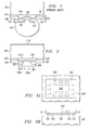
- FIG. 2 illustrates the first preferred embodiment of the present invention.
- 201 is a portion of the semiconductor chip, with planar active surface 201a, including an integrated circuit (IC).
- the semiconductor material is commonly silicon; other materials include silicon germanium, gallium arsenide, or any other semiconductor material used in IC fabrication.
- the IC has a metallization pattern 202 including a plurality of contact pads 202a.
- the chip metallization 202 may consist of aluminum, copper, or alloys thereof.
- the IC surface is protected by a dielectric protective overcoat 203, usually silicon nitride of about 1 ⁇ m thickness. Also shown in FIG.
- FIG. 2 is an optional polymeric overcoat 204, frequently benzocyclobutene (BCB) in the thickness range between 1 to 3 ⁇ m.
- BCB benzocyclobutene
- the contact pad When layer 202 is aluminum or aluminum alloyed with 0.5 to 2 % copper and/or 0.5 to 1 % silicon (layer 0.4 to 1.5 ⁇ m thick), the contact pad exhibits under the aluminum frequently a thin layer (4 to 20 nm thick) of titanium, titanium nitride, titanium tungsten, tantalum, tantalum nitride, tantalum silicon nitride, tungsten nitride, or tungsten silicon nitride (not shown in FIG. 2).
- the insulator under the metallization is typically silicon dioxide.
- films made of silicon-containing hydrogen silsesquioxane (HSQ), aerogels, organic polyimides and parylenes are also used in spite of the fact that they are less dense and mechanically weaker than previous standard insulators such as the plasma-enhanced chemical vapor deposited dielectrics.
- stacks of dielectric layers may be used such as alternating layers of plasma-generated tetraethylorthosilicate (TEOS) oxide and HSQ, or ozone TEOS oxide and HSQ.
- the contact pad has an added conductive layer 205 on the pad metallization 202.
- This layer 205 is conformal to the surface of the chip and provides a reliable, low resistance contact to the pad metallization 202.
- layer 205 covers not only the area of the pad 202a proper, but also the window side walls of protective layers 203 and 204 and a portion 205a of the surface surrounding the pad window.
- the preferred material for layer 205 is aluminum in the thickness range of about 500 to 1000 nm.
- the second added layer 206 in FIG. 2 has the important function to enable the transition from a conformal outline following the chip surface contours, to a "flat" outline defining a planar outer surface, which is substantially parallel to the chip surface.
- the second conductive layer 206 may also have to operate as a diffusion barrier if copper is used as the chip metallization 202.
- the second conductive layer is selected from a group consisting of nickel, vanadium, titanium, tungsten, tantalum, osmium, chromium, and aluminum, and alloys thereof.
- the outermost metal layer 207 has a surface suitable to form metallurgical bonds without melting.
- layer 207 is made of a metal selected from a group consisting of gold, palladium, platinum, silver, and alloys thereof.
- the bondability function of layer 207 is emphasized.
- the overall thickness of the bondable metal layer 207 usually a noble metal, is kept to a minimum, thus saving cost. Acceptable thicknesses range from about 0.02 to 0.1 ⁇ m; for some metals, a flash is sufficient.
- these surfaces are suitable for the following attaching methods to outside board surfaces, which have been prepared with appropriately bondable metal surfaces (typically gold flash on copper-metallized terminal pads):
- the number of added conductive layers are not restricted to three. There may be only one layer, or two layers, or more than three layers added to the chip contact pads metallization. It is only required that the added conductive layer or layers have a conformal surface adjacent the chip and a planar outer surface, and that the puter surface be suitable to form metallurgical bonds, without necessarily resorting to melting of solder.
- the described added conductive layers can be formed onto any number of chip contact pads.
- the described technique is thus applicable chips with a small number of I/O's (for example, 12 I/O's as illustrated in FIG. 3) as well as to chips with a high number of I/O's (for example, 200 or 600 I/O's).
- the contact pads may be shaped as a rectangle, a square or a circle with a side length of about 40 to 150 ⁇ m, preferably 90 to 100 ⁇ m.
- the pitch between neighboring contact pads is typically in the range from 0.4 to 0.6 mm with a separation between pads from 50 to 200 ⁇ m, for chips with high numbers of input/output terminals preferably between 50 and 75 ⁇ m. It is a technical advantage of the present invention that the pitch between neighboring contacts can be reduced to 100 ⁇ m center-to-center, which is a major improvement over solder ball contacts.
- the described added conductive layers can be formed whatever the arrangement and distribution of the contact pads may be.
- the contact pads may be arrayed along the periphery of the active chip surface, as illustrated in FIG. 3.
- the contact pads may be arrayed in the center of the active chip surface.
- the contact pads may be arrayed in an arbitrary configuration across the active chip surface.
- layer 210 is an electrically non-conductive material of black color to protect the chip against disturbing influences of light or other electro-magnetic radiation, of environmental degradation such as moisture and dust, and of mechanical disturbances such as scratches.
- Meethods of fabricating layer 210 include:
- FIG. 3 illustrates the second preferred embodiment of the invention in a schematic top view (FIG. 3A) of the active chip surface 301 and a schematic cross section (FIG. 3B) of the chip attached to the wiring board.
- the chip contact pads 302, covered with the added conductive layers described above are distributed such that an area portion of the active chip surface is available for attaching a thermally conductive plate 303.
- this area portion is the central area of the active chip surface 301.
- the plate is operable as a heat spreader, it is preferably made of a good thermal conductor (yet low cost material) such as copper and has a thickness compatible with the thickness of the added conductive pads layers (0.2 to 0.8 ⁇ m).
- the plate 303 has an outer surface suitable for metallurgical bonds. Especially, the outer surface may be solderable. Preferably, the outer plate surface is a noble metal layer similar to layer 207 in FIG. 2, for instance a gold flash.
- the plate can then be attached to a wiring board metal pad, pre-fabricated in aligned position, concurrently with the attachment of the contact metal structures 302 to the board. For this attachment to the board, the same options are available, which are discussed above:
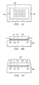
- the contact pads may be arrayed in the center of the active chip surface. This case is depicted in FIGs. 4A and 4B, with the contact pads 402 and 411, respectively, in the center of the surface 401 of chip 410.
- the area portion of the active chip surface available for attaching a thermally conductive plate is the chip periphery.
- the heat spreader is now formed as a broad frame 403 and 412, respectively, around the contact pads. This distribution is particularly favorable for minimizing thermomechanical stress at the assembled contact pads, when the system is subjected to temperature variations and the mismatch between the coefficients of thermal expansion of IC chip and board become important.
- the mirror-image metallized areas on board 420 are designated 421 for the contact pads and 422 for the heat-conducting frame.
- an encapsulation can be formed protecting at least the chip surface opposite to the active surface, and that the encapsulated device can be assembled on a board.
- the preferred encapsulation material is a molding compound, and the preferred encapsulation method the transfer molding technique.
- the device variation exhibiting a molded encapsulation is especially recommended when the I/C chip is thinner than the customary thickness of 275 ⁇ m.
- FIG. 4C shows the assembly of FIG. 4B with a device having an encapsulation 430.
- FIGs. 5 and 6 a molded device analogous to the embodiment in FIG. 3B is shown in an assembly on relatively thin substrates, preferably insulator-based substrates such as a polyimide film.
- this assembled device is then completed as a ball-grid array device having solder balls.
- the assembled device is completed as a land-grid array (lead-less, or no-lead) device having bondable or solderable attachment pads.
- the I/C chip 510 has added conductive contact metallization 511 for the plurality of pads and a heat spreader 512 similar to FIG. 3B. Molding compound 513 encapsulates the device.
- the film-like substrate 520 has mirror-image terminals 521 for the contact pads 511 and heat sink 522 for heat spreader 511. Molding compound 513 encapsulates the passive surface of the chip, attaches strongly to substrate 520, and fills the gaps 530. Using solder balls 540, the device is attached to printed circuit board 550.
- bondable or solderable lands replace the solder balls 540 of FIG. 5.
- the structure of the device and the assembly onto the board are analogous to FIG. 5.
- the contact metallization 711 of chip 710 is attached to the counterparts 721 on a "leadframe"-like, relatively thick sheet of metal 720.
- This sub-assembly is encapsulated in molding compound 713, which also fill the gaps 730.
- the outer surface of the sheet-like metal 721 is bondable or solderable. It is attached to printed circuit board 750.
- FIG. 7 lends itself to fabricating a chip-size package. Instead of encapsulating individual chips, the whole wafer is encapsulated by molding compound. Subsequently, the devices are singulated, preferably by sawing, along lines 714, which are determined by the outline of chip 710.
Landscapes
- Engineering & Computer Science (AREA)
- Power Engineering (AREA)
- Microelectronics & Electronic Packaging (AREA)
- Chemical & Material Sciences (AREA)
- Combustion & Propulsion (AREA)
- Wire Bonding (AREA)
- Rectifiers (AREA)
- Synchronous Machinery (AREA)
Abstract
Description
- Direct welding by metallic interdiffusion;
- Attaching by solder paste;
- Attaching by conductive adhesive.
- a highly ductile solder;
- a high ultimate shear strength of the chip/joint and substrate/joint interfaces;
- a large value for the ratio (radius of bump-to-chip contact)/(distance to neutral point of chip).
- Electroless plating. The complete process includes the
following steps:
- Coating the backside of the silicon IC wafer with resist using a spin-on technique. This coat will prevent accidental metal deposition on the wafer backside.
- Baking the resist, typically at 110 °C for a time period of about 30 to 60 minutes.
- Cleaning of the exposed bond pad metal surface using a plasma ashing process for about 2 minutes.
- Cleaning by immersing the wafer, having the exposed metal of the bond pads, in a solution of sulfuric acid, nitric acids, or any other acid, for about 50 to 60 seconds.
- Rinsing in overflow rinser for about 100 to 180 seconds.
- Immersing the wafer in a catalytic metal chloride solution, such as palladium chloride, for about 40 to 80 seconds "activates" the metal surface, i.e., a layer of seed metal (such as palladium) is deposited onto the clean non-oxidized metal surface.
- Rinsing in dump rinser for about 100 to 180 seconds.
- Electroless plating of the barrier metal. If nickel is selected, plating between 150 to 180 seconds will deposit about 0.4 to 0.6 µm thick nickel.
- Screen printing. A plurality of openings are prepared in a mask stencil so that their position mirror-images the position of the contact pads on the IC surface. The mask stencil is then aligned with the semiconductor wafer so that each mask opening aligns with its respective IC contact pad. The metal or metal alloy is liquefied and deposited through the mask openings so that it equalizes the overcoat contours of the pad window remaining from the etch step through the overcoat layers.
- Support by islands of protective overcoat. Applying a modification of the U.S. Patent Application # 09/458,593 cited above, the contact pads are opened so that a plurality of silicon nitride "islands" remain unetched in the window area, creating numerous silicon nitride "mesas" with narrow vias between them. In the following metal deposition step (for instance, aluminum as the first layer, nickel as the second layer), the vias are quickly filled, while metal is also deposited on top of the mesas. The overall window metal surface approaches progressively a uniformly flat configuration.
- Direct welding by metallic interdiffusion. For this bonding, the clean surfaces of the chip contact and board terminal pads are subjected to slight compression or thermo-compression at elevated temperatures and moderate pressures for a period of time on the order of 1 s.
- Attachment by conductive adhesives. This preferred embodiment permits small pad sizes and fine pad pitch, since conductive adhesives do not tend to bridge.
- Attachment by solder paste. Both the chip contact pads and the board terminal pads are solderable. Consequently, metallurgically strong solder connections are easily established.
- Screen-printing of polymeric material, undoped or doped;
- Spinning of insulating material which will harden;
- Attaching tape or film;
- Spraying low-viscosity material which will harden; and
- Transfer molding a protective layer.
- Direct welding by metallic interdiffusion;
- Attachment by conductive adhesives;
- Attachment by solder paste.
Claims (10)
- A semiconductor device comprising:a semiconductor chip having a planar active surface including an integrated circuit, said circuit having metallization patterns including a plurality of contact pads;each of said contact pads having an added conductive layer on said metallization, said added layer having a conformal surface adjacent said chip and a planar outer surface, said outer surface suitable to form metallurgical bonds without melting.
- The device according to Claim 1 wherein said conductive layer consists of at least two conductive sub-layers, one being a conductive diffusion barrier, the other, outer layer being bondable.
- The device according to Claim 2 wherein said conductive diffusion barrier is selected from a group consisting of nickel, vanadium, titanium, tungsten, tantalum, osmium, chromium, and aluminum.
- The device according to Claim 2 or claim 3 wherein said bondable
layer is selected from a group consisting of gold, palladium, platinum, silver, and alloys thereof. - The device according to any preceding Claim further comprising:a distribution of said contact pads such that an area portion of said active chip surface is available for attaching a thermally conductive plate, said plate having a thickness compatible with the thickness of said conductive pad layer.
- A method for fabricating a semiconductor device having a semiconductor chip including a planar active surface and a metallization pattern including a plurality of contact pads, comprising the step of:depositing at least one added conductive layer on said metallization of said contact pads, said added layer having a conformal surface adjacent said chip and a planar outer surface, said outer surface suitable to form metallurgical bonds without melting.
- The method according to Claim 6 wherein said step of depositing is selected from a group consisting of sputtering, evaporating, and plating.
- The method according to Claim 6 or Claim 7 wherein said step of
fabricating a planar outer surface of said added layer comprises the step of depositing said at least one added conductive layer by electroless plating. - The method according to Claim 6, Claim 7, or Claim8 wherein said step of
fabricating a planar outer surface of said added layer comprises the step of depositing said at least one added conductive layer by screen printing. - The method according to Claim 6, Claim 7, Claim 8 or Claim 9 wherein said step of
fabricating a planar outer surface of said added layer comprises the step of depositing said at least one added conductive layer by using the method of support by islands of protective overcoat.
Applications Claiming Priority (2)
| Application Number | Priority Date | Filing Date | Title |
|---|---|---|---|
| US11302 | 2001-11-06 | ||
| US10/011,302 US6621703B2 (en) | 1998-10-07 | 2001-11-06 | Automotive bridge rectifier assembly with thermal protection |
Publications (3)
| Publication Number | Publication Date |
|---|---|
| EP1316998A2 true EP1316998A2 (en) | 2003-06-04 |
| EP1316998A3 EP1316998A3 (en) | 2005-02-02 |
| EP1316998B1 EP1316998B1 (en) | 2021-04-28 |
Family
ID=21749772
Family Applications (1)
| Application Number | Title | Priority Date | Filing Date |
|---|---|---|---|
| EP02102521.8A Expired - Lifetime EP1316998B1 (en) | 2001-11-06 | 2002-10-31 | Bumpless Chip Scale Device (CSP) and board assembly |
Country Status (2)
| Country | Link |
|---|---|
| US (1) | US6621703B2 (en) |
| EP (1) | EP1316998B1 (en) |
Cited By (3)
| Publication number | Priority date | Publication date | Assignee | Title |
|---|---|---|---|---|
| EP1333494A3 (en) * | 2002-01-25 | 2006-06-07 | Texas Instruments Incorporated | Semiconductor device and method of fabricating a semiconductor assembly |
| US9480185B2 (en) | 2014-01-08 | 2016-10-25 | Enphase Energy, Inc. | Double insulated heat spreader |
| US20230359856A1 (en) * | 2020-09-25 | 2023-11-09 | Linxens Holding | Prelam body of a smart card, method of forming a prelam body of a smart card, and a smart card |
Families Citing this family (12)
| Publication number | Priority date | Publication date | Assignee | Title |
|---|---|---|---|---|
| US6327128B1 (en) * | 1998-10-07 | 2001-12-04 | Electro-Dyn Electronics Corporation | Automotive bridge rectifier assembly with thermal protection |
| US7292445B2 (en) * | 2003-02-25 | 2007-11-06 | Siliconix Technology C.V.-Ir | Active integrated rectifier regulator |
| US7612474B2 (en) * | 2004-12-21 | 2009-11-03 | Electric-Dyn Choke Corporation | Rectifier assembly with enhanced air cooling |
| JP4400577B2 (en) * | 2006-01-20 | 2010-01-20 | 株式会社デンソー | AC generator for brushless vehicles |
| US20070206363A1 (en) * | 2006-03-01 | 2007-09-06 | Wetherill Associates, Inc., Corporation Of The State Of Delaware | Voltage regulator with welded lead frame connectors and method of making |
| US8072191B2 (en) * | 2008-01-02 | 2011-12-06 | Hamilton Sundstrand Corporation | Shorted rotating diode detection and protection |
| US9318936B2 (en) * | 2010-07-21 | 2016-04-19 | Romaine Electric | Alternator stator lead and terminal insulator assembly |
| DE102011003896A1 (en) * | 2011-02-10 | 2012-08-16 | Robert Bosch Gmbh | Electrical generator operating device for vehicle, has field controller for adjustment of exciting current of electrical generator, where rectifier and field controller are thermally coupled to common over-temperature protective device |
| US9082737B2 (en) * | 2012-11-15 | 2015-07-14 | Infineon Technologies Ag | System and method for an electronic package with a fail-open mechanism |
| CN105793985B (en) * | 2013-12-17 | 2019-02-12 | 西门子公司 | Electronic Protection Modules for HVDC Converters |
| DE202014004732U1 (en) | 2014-06-12 | 2014-07-04 | Brose Fahrzeugteile GmbH & Co. Kommanditgesellschaft, Würzburg | Electric motor with thermal fuse |
| JP7477958B2 (en) * | 2019-10-30 | 2024-05-02 | デクセリアルズ株式会社 | Protection elements and circuits |
Family Cites Families (37)
| Publication number | Priority date | Publication date | Assignee | Title |
|---|---|---|---|---|
| US3684944A (en) | 1971-07-09 | 1972-08-15 | Ni I Exi Aoromobilnogg Elecktr | Rectifier for an electric generator |
| JPS4943722U (en) | 1972-07-21 | 1974-04-17 | ||
| US3778650A (en) | 1972-10-10 | 1973-12-11 | Briggs & Stratton Corp | Battery charging regulator-rectifier module |
| US3812390A (en) | 1973-07-13 | 1974-05-21 | Wagner Electric Corp | Alternator rectifier |
| US3959676A (en) | 1974-12-23 | 1976-05-25 | Ford Motor Company | Alternator rectifier bridge and method of assembly |
| DE2511636C3 (en) | 1975-03-17 | 1980-04-17 | Kraftwerk Union Ag, 4330 Muelheim | Rotating rectifier arrangement for excitation systems for electrical machines |
| GB1557666A (en) | 1975-12-20 | 1979-12-12 | Lucas Industries Ltd | Multiphase full wave rectifier assembly |
| GB1589717A (en) | 1976-10-22 | 1981-05-20 | Lucas Industries Ltd | Multiphase full-wave rectifier assembly |
| JPS5432740A (en) | 1977-08-17 | 1979-03-10 | Mitsubishi Electric Corp | Device for detecting break of fuse |
| GB1599898A (en) | 1977-10-29 | 1981-10-07 | Lucas Industries Ltd | Multiphase full-wave rectifier assembly |
| DE2847501A1 (en) | 1978-11-02 | 1980-05-14 | Bosch Gmbh Robert | ELECTRIC GENERATOR |
| DE2847502A1 (en) | 1978-11-02 | 1980-05-14 | Bosch Gmbh Robert | ELECTRIC GENERATOR |
| US4221456A (en) | 1979-03-01 | 1980-09-09 | Ford Motor Company | Fuse holder for an automotive fuse terminal block |
| FR2473801A1 (en) | 1979-12-13 | 1981-07-17 | Bosch Gmbh Robert | BLOCK OF DIODES |
| JPH0119584Y2 (en) | 1980-05-09 | 1989-06-06 | ||
| US4635044A (en) | 1980-10-16 | 1987-01-06 | Westinghouse Electic Corp. | Failed fuse detector and detecting method for rotating electrical equipment |
| US4543504A (en) | 1982-10-13 | 1985-09-24 | Mitsubishi Denki Kabushiki Kaisha | Electric current rectifier |
| US4606000A (en) | 1985-03-27 | 1986-08-12 | General Motors Corporation | Bridge rectifier |
| JPS62144346A (en) * | 1985-12-19 | 1987-06-27 | Matsushita Electric Ind Co Ltd | Semiconductor integrated circuit element |
| DE3728081A1 (en) | 1987-08-22 | 1989-03-02 | Bosch Gmbh Robert | RECTIFIER BEARING DEVICE |
| US4799309A (en) * | 1987-12-24 | 1989-01-24 | Ford Motor Company | Method of making a rectifier and control module for an alternator |
| US5055058A (en) | 1989-05-30 | 1991-10-08 | Yazaki Corporation | Device for checking for incomplete locking of connector housings |
| US5043614A (en) | 1990-02-02 | 1991-08-27 | Ford Motor Company | Alternator rectifier bridge assembly |
| US5005069A (en) | 1990-04-30 | 1991-04-02 | Motorola Inc. | Rectifier and method |
| US5451823A (en) | 1993-02-11 | 1995-09-19 | Transpo Electronics, Inc. | Vehicular thermoconductive lead frame rectifier assembly |
| US5249728A (en) * | 1993-03-10 | 1993-10-05 | Atmel Corporation | Bumpless bonding process having multilayer metallization |
| US5453901A (en) | 1993-10-12 | 1995-09-26 | General Electric Co. | Detection and protection of excitation system from diode failure |
| US5466635A (en) * | 1994-06-02 | 1995-11-14 | Lsi Logic Corporation | Process for making an interconnect bump for flip-chip integrated circuit including integral standoff and hourglass shaped solder coating |
| US5659212A (en) * | 1994-12-16 | 1997-08-19 | Electro-Dyn Choke Corporation | Rectifier assembly for automotive alternator |
| JP3342978B2 (en) * | 1994-12-27 | 2002-11-11 | 三菱電機株式会社 | AC generator for vehicles |
| US5693565A (en) * | 1996-07-15 | 1997-12-02 | Dow Corning Corporation | Semiconductor chips suitable for known good die testing |
| FR2757327B1 (en) | 1996-12-16 | 1999-01-22 | Valeo Equip Electr Moteur | MOTOR VEHICLE ALTERNATOR WITH WATER COOLED REAR BEARING |
| BR9802812A (en) | 1997-08-29 | 1999-11-03 | Whitaker Corp | short-circuit terminal and connector. |
| JP3430016B2 (en) | 1998-06-05 | 2003-07-28 | 三菱電機株式会社 | AC generator for vehicles |
| US6327128B1 (en) | 1998-10-07 | 2001-12-04 | Electro-Dyn Electronics Corporation | Automotive bridge rectifier assembly with thermal protection |
| US5991184A (en) * | 1999-03-02 | 1999-11-23 | Transpo Electronics, Inc. | Vehicular extended thermal cycle minimal part robust rectifier assembly |
| US20010033020A1 (en) * | 2000-03-24 | 2001-10-25 | Stierman Roger J. | Structure and method for bond pads of copper-metallized integrated circuits |
-
2001
- 2001-11-06 US US10/011,302 patent/US6621703B2/en not_active Expired - Fee Related
-
2002
- 2002-10-31 EP EP02102521.8A patent/EP1316998B1/en not_active Expired - Lifetime
Cited By (5)
| Publication number | Priority date | Publication date | Assignee | Title |
|---|---|---|---|---|
| EP1333494A3 (en) * | 2002-01-25 | 2006-06-07 | Texas Instruments Incorporated | Semiconductor device and method of fabricating a semiconductor assembly |
| US9480185B2 (en) | 2014-01-08 | 2016-10-25 | Enphase Energy, Inc. | Double insulated heat spreader |
| US10098261B2 (en) | 2014-01-08 | 2018-10-09 | Enphase Energy, Inc. | Double insulated heat spreader |
| US20230359856A1 (en) * | 2020-09-25 | 2023-11-09 | Linxens Holding | Prelam body of a smart card, method of forming a prelam body of a smart card, and a smart card |
| US12190188B2 (en) * | 2020-09-25 | 2025-01-07 | Linxens Holding | Prelam body of a smart card, method of forming a prelam body of a smart card, and a smart card |
Also Published As
| Publication number | Publication date |
|---|---|
| US6621703B2 (en) | 2003-09-16 |
| EP1316998A3 (en) | 2005-02-02 |
| US20020041476A1 (en) | 2002-04-11 |
| EP1316998B1 (en) | 2021-04-28 |
Similar Documents
| Publication | Publication Date | Title |
|---|---|---|
| US6914332B2 (en) | Flip-chip without bumps and polymer for board assembly | |
| US6768210B2 (en) | Bumpless wafer scale device and board assembly | |
| US7187078B2 (en) | Bump structure | |
| US7665652B2 (en) | Electronic devices including metallurgy structures for wire and solder bonding | |
| US6459150B1 (en) | Electronic substrate having an aperture position through a substrate, conductive pads, and an insulating layer | |
| US6413862B1 (en) | Use of palladium in IC manufacturing | |
| US7314817B2 (en) | Microelectronic device interconnects | |
| EP1387402A2 (en) | Wafer-level method for fine-pitch, high aspect ratio chip interconnect | |
| US6667557B2 (en) | Method of forming an apparatus to reduce thermal fatigue stress on flip chip solder connections | |
| US11894330B2 (en) | Methods of manufacturing a semiconductor device including a joint adjacent to a post | |
| US6914333B2 (en) | Wafer level package incorporating dual compliant layers and method for fabrication | |
| US20040087057A1 (en) | Method for fabricating a flip chip package with pillar bump and no flow underfill | |
| US7271498B2 (en) | Bump electrodes having multiple under ball metallurgy (UBM) layers | |
| US6597070B2 (en) | Semiconductor device and method of manufacturing the same | |
| EP1316998B1 (en) | Bumpless Chip Scale Device (CSP) and board assembly | |
| US20050151268A1 (en) | Wafer-level assembly method for chip-size devices having flipped chips | |
| US20060286791A1 (en) | Semiconductor wafer package and manufacturing method thereof | |
| US7906425B2 (en) | Fluxless bumping process | |
| US6664176B2 (en) | Method of making pad-rerouting for integrated circuit chips | |
| US20250309074A1 (en) | Package assembly including package substrate with elongated solder resist opening and methods for forming the same | |
| WO2012177450A1 (en) | Semiconductor chip with dual polymer film interconnect structures | |
| US20060022320A1 (en) | Semiconductor device and manufacturing method thereof | |
| US20040266066A1 (en) | Bump structure of a semiconductor wafer and manufacturing method thereof | |
| US7910471B2 (en) | Bumpless wafer scale device and board assembly | |
| US9842819B2 (en) | Tall and fine pitch interconnects |
Legal Events
| Date | Code | Title | Description |
|---|---|---|---|
| PUAI | Public reference made under article 153(3) epc to a published international application that has entered the european phase |
Free format text: ORIGINAL CODE: 0009012 |
|
| AK | Designated contracting states |
Designated state(s): AT BE BG CH CY CZ DE DK EE ES FI FR GB GR IE IT LI LU MC NL PT SE SK TR |
|
| AX | Request for extension of the european patent |
Extension state: AL LT LV MK RO SI |
|
| PUAL | Search report despatched |
Free format text: ORIGINAL CODE: 0009013 |
|
| AK | Designated contracting states |
Kind code of ref document: A3 Designated state(s): AT BE BG CH CY CZ DE DK EE ES FI FR GB GR IE IT LI LU MC NL PT SE SK TR |
|
| AX | Request for extension of the european patent |
Extension state: AL LT LV MK RO SI |
|
| 17P | Request for examination filed |
Effective date: 20050802 |
|
| AKX | Designation fees paid |
Designated state(s): DE FR GB |
|
| STAA | Information on the status of an ep patent application or granted ep patent |
Free format text: STATUS: EXAMINATION IS IN PROGRESS |
|
| GRAP | Despatch of communication of intention to grant a patent |
Free format text: ORIGINAL CODE: EPIDOSNIGR1 |
|
| STAA | Information on the status of an ep patent application or granted ep patent |
Free format text: STATUS: GRANT OF PATENT IS INTENDED |
|
| INTG | Intention to grant announced |
Effective date: 20201130 |
|
| GRAS | Grant fee paid |
Free format text: ORIGINAL CODE: EPIDOSNIGR3 |
|
| GRAA | (expected) grant |
Free format text: ORIGINAL CODE: 0009210 |
|
| STAA | Information on the status of an ep patent application or granted ep patent |
Free format text: STATUS: THE PATENT HAS BEEN GRANTED |
|
| AK | Designated contracting states |
Kind code of ref document: B1 Designated state(s): DE FR GB |
|
| REG | Reference to a national code |
Ref country code: GB Ref legal event code: FG4D |
|
| REG | Reference to a national code |
Ref country code: DE Ref legal event code: R096 Ref document number: 60250227 Country of ref document: DE |
|
| REG | Reference to a national code |
Ref country code: DE Ref legal event code: R097 Ref document number: 60250227 Country of ref document: DE |
|
| PLBE | No opposition filed within time limit |
Free format text: ORIGINAL CODE: 0009261 |
|
| STAA | Information on the status of an ep patent application or granted ep patent |
Free format text: STATUS: NO OPPOSITION FILED WITHIN TIME LIMIT |
|
| 26N | No opposition filed |
Effective date: 20220131 |
|
| REG | Reference to a national code |
Ref country code: DE Ref legal event code: R119 Ref document number: 60250227 Country of ref document: DE |
|
| GBPC | Gb: european patent ceased through non-payment of renewal fee |
Effective date: 20211031 |
|
| PG25 | Lapsed in a contracting state [announced via postgrant information from national office to epo] |
Ref country code: GB Free format text: LAPSE BECAUSE OF NON-PAYMENT OF DUE FEES Effective date: 20211031 Ref country code: DE Free format text: LAPSE BECAUSE OF NON-PAYMENT OF DUE FEES Effective date: 20220503 |
|
| PG25 | Lapsed in a contracting state [announced via postgrant information from national office to epo] |
Ref country code: FR Free format text: LAPSE BECAUSE OF NON-PAYMENT OF DUE FEES Effective date: 20211031 |