EP1316997B1 - Umrichter in Druckkontaktierung - Google Patents
Umrichter in Druckkontaktierung Download PDFInfo
- Publication number
- EP1316997B1 EP1316997B1 EP02026281A EP02026281A EP1316997B1 EP 1316997 B1 EP1316997 B1 EP 1316997B1 EP 02026281 A EP02026281 A EP 02026281A EP 02026281 A EP02026281 A EP 02026281A EP 1316997 B1 EP1316997 B1 EP 1316997B1
- Authority
- EP
- European Patent Office
- Prior art keywords
- lugs
- converter according
- contacting
- contact
- warts
- Prior art date
- Legal status (The legal status is an assumption and is not a legal conclusion. Google has not performed a legal analysis and makes no representation as to the accuracy of the status listed.)
- Expired - Lifetime
Links
Images


Classifications
-
- H—ELECTRICITY
- H10—SEMICONDUCTOR DEVICES; ELECTRIC SOLID-STATE DEVICES NOT OTHERWISE PROVIDED FOR
- H10W—GENERIC PACKAGES, INTERCONNECTIONS, CONNECTORS OR OTHER CONSTRUCTIONAL DETAILS OF DEVICES COVERED BY CLASS H10
- H10W72/00—Interconnections or connectors in packages
-
- H—ELECTRICITY
- H10—SEMICONDUCTOR DEVICES; ELECTRIC SOLID-STATE DEVICES NOT OTHERWISE PROVIDED FOR
- H10W—GENERIC PACKAGES, INTERCONNECTIONS, CONNECTORS OR OTHER CONSTRUCTIONAL DETAILS OF DEVICES COVERED BY CLASS H10
- H10W90/00—Package configurations
Definitions
- the invention relates to a converter in pressure contact consisting of a main body, a substrate arranged thereon interconnected semiconductor devices and provided on this substrate contact points, power supply elements for DC and AC voltage connections for contacting these contact points and for contacting a DC intermediate circuit and the AC power connection.
- Warts are known on the contact points of the intermediate circuit, which are contacted by means of a flat-shaped connection element.
- the disadvantage here is that the warts in part have a different height and therefore the contact is not made with all warts or at least not completely.
- Even more crucial is that the warts have only a small common contact surface with the planar surface of the connection element by their spherical segment-like shape. This limits the current carrying capacity Such compounds crucial because the current-carrying surface is a direct measure of the current carrying capacity.
- planar contact points for example, the contact points of the substrate and elevations on the connecting elements with a sawtooth-shaped contact surface facing surface.
- the main disadvantage of this embodiment is also the small contact surface and thus the insufficient current carrying capacity of these compounds.
- the US 5,329,423 discloses a low power connector wherein the components to be connected are exemplary integrated circuits (IC) in multi-chip modules.
- IC integrated circuits
- individual contact devices are exemplified by a component (IC) formed by warts, which have a common contact surface with corresponding receptacles of a counterpart to be contacted.
- the present invention has for its object to provide a converter, wherein the main terminals are designed in pressure contact and the contact surfaces are as large as possible to ensure high current carrying capacity and to allow a low-inductive coupling.
- the basic idea of the invention lies in the deformation of warts by the pressure contacting of the power semiconductor module.
- deformable warts are applied to the contact points, which are only partially covered by a plurality of elevations of the connection elements.
- the pressure contact of these warts they are deformed so that they conform to the contour of the surveys of the Adapt connection elements and thus form the largest possible common surface with them. This directly benefits the current-carrying capacity of these compounds.
- Another advantage of the invention lies in the compensation of small height differences of individual warts and / or individual elevations of the connecting elements to each other, since the warts are deformed by the pressure contact and thus a secure and flat contact is made.
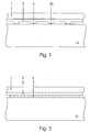
- Fig. 1 shows an embodiment of power connection elements for contacting within a converter according to the prior art.
- Fig. 2 shows a further embodiment of power connection elements for contacting within a converter according to the prior art.
- Fig. 3 shows the inventive design of the individual parts of power supply elements for contacting within an inverter.
- Fig. 4 shows the operation of the inventive design of power connector elements for contacting within an inverter.
- Fig. 5 shows a further embodiments of inventive power connector elements for contacting.
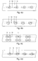
- Fig. 6 shows various embodiments of inventive power connector elements for contacting in plan view.
- Fig. 1 shows an embodiment of power connection elements (21) for contacting within a converter according to the prior art.
- the counterpart (1) of the power connection elements (21) for contacting has a conductive layer (3) with warts (4) arranged thereon, which in the case of pressure contact of the converter, the electrically conductive connection between the power connection elements (21) for contacting and their respective counterpart (1) produce.
- the conductive surface is limited to the very small contact surface (22).
- Fig. 2 shows a further embodiment of power connection elements for contacting within a converter according to the prior art.
- the current connection element for contacting (21) is connected directly to the conductive layer (3) of the corresponding counterpart (1) by means of a material connection (for example solder).
- Fig. 3 shows the inventive design of the individual parts of power supply elements (10) for contacting within an inverter.
- the current connection element (10) designed as a one-piece metal press part for contacting has elevations (11) (FIG. 3c).
- the counterpart (1) has, for example, an electrically conductive layer located inside it with connections to the surface facing the power connection elements (10) for contacting. On these connections, electrically-connected warts (4) made of soft solder are arranged with them (FIG. 3b).
- a further embodiment (FIG. 3 a) of the counterpart (1) of the current connection elements (10) for contacting corresponds to that already described in FIG. 1 with an electrically conductive layer (3) on the side facing the power connection elements for contacting and warts (4 ).
- Fig. 4 shows the operation of the inventive design of power connector elements for contacting within an inverter.
- the current connection element for contacting (10) is arranged in such a way to its counterpart (1), that the elevations (11) of the power connection elements for contacting (10) not completely cover the base of the warts (4), but have a lateral offset.
- the warts (4) are partially deformed by the elevations (11) such that a contact surface (12) results between the elevations (11) and the warts (4), which in their entirety at least one fifth of the base of the warts (4).
- Fig. 5 shows a further embodiment of the inventive power connector elements (10) for contacting.
- the base of the elevations (11) is smaller than the base area the warts (4) ( Figure 5a). This also results in a deformation of the warts (4) such that the respective contact surface (12) is greater than one-fifth of the wart base after pressure introduction of the pressure-contacted structure (FIG. 5b).
- Fig. 6 shows various embodiments of the inventive power connector elements (10) for contacting in plan view.
- the proportion, parallel to the surface of the counterpart (1) of the power connection elements (10) for contacting, the contact surface (12) between the elevations (11) and the warts (4 ) and their arrangement in series clearly visible.
- Fig. 6b shows an embodiment with an offset of the warts (4) to the power connection elements (10) for contacting not in the direction of the longitudinal extent of the power connection elements for contacting, but orthogonal thereto.
- Fig. 6c shows a further inventive embodiment such that a survey not only a wart (4) but two warts are assigned. Furthermore, the warts (4) and their associated elevations (11) are arranged like a matrix.
- FIG. 6d shows that in each case one wart (4) has two elevations (11) associated therewith.
Landscapes
- Inverter Devices (AREA)
- Switches Operated By Changes In Physical Conditions (AREA)
- Secondary Cells (AREA)
- Contacts (AREA)
- Die Bonding (AREA)
- Coupling Device And Connection With Printed Circuit (AREA)
- Wire Bonding (AREA)
Description
- Die Erfindung betrifft einen Umrichter in Druckkontaktierung bestehend aus einem Grundkörper, einem Substrat mit darauf angeordneten schaltungsgerecht miteinander verbunden Halbleiterbauelementen sowie auf diesem Substrat vorgesehenen Kontaktstellen, Stromanschlusselementen für Gleich- und Wechselspannungsanschlüsse zur Kontaktierung dieser Kontaktstellen sowie zur Kontaktierung eines Gleichstromzwischenkreises und des Wechselstromanschlusses.
- Derartige druckkontaktierte Schaltungsanordnungen werden beispielhaft in der
DE 101 27 947 offenbart. Bei Umrichtern der Leistungsklasse besonders wichtige Aspekte sind eine niederinduktive Stromzufuhr aus dem Zwischenkreis sowie eine hohe Stromtragfähigkeit aller Komponenten der Leistungsanschlüsse, d.h. der Plus- und Minusanschlüsse des Zwischenkreises sowie der Wechselstromanschlüsse. In druckkontaktierten Umrichtern bilden den Stand der Technik verschiedene Verbindungstechniken zwischen den verschieden Kontaktstellen, z.B. auf dem Substrat oder auf der Zwischenkreisplatine und mit den Stromanschlusselementen. - Bekannt sind Warzen auf den Kontaktstellen des Zwischenkreises, die mittels eines flächig ausgebildeten Anschlusselements kontaktiert werden. Nachteilig ist hierbei, dass die Warzen zum Teil eine unterschiedliche Höhe aufweisen und daher der Kontakt nicht mit allen Warzen oder zumindest nicht vollständig hergestellt wird. Noch entscheidender ist, dass die Warzen durch ihre kugelsegmentartige Form nur eine geringe gemeinsame Kontaktfläche mit der planen Oberfläche des Anschlusselements aufweisen. Dies schränkt die Stromtragfähigkeit derartiger Verbindungen entscheidend ein, da die stromdurchflossene Fläche ein direktes Maß für die Stromtragfähigkeit darstellt.
- Ebenfalls bekannt sind plane Kontaktstellen beispielhaft die Kontaktstellen des Substrats sowie Erhebungen auf den Anschlusselementen mit einer sägezahnartig ausgebildeten der Kontaktstelle zugewandten Oberfläche. Der wesentliche Nachteil dieser Ausgestaltung ist ebenfalls die geringe Kontaktfläche und damit die ungenügende Stromtragfähigkeit dieser Verbindungen.
- Eine weitere nach dem Stand der Technik bekannte Verbindung ist die stoffschlüssige Verbindung, wie sie beispielhaft durch Löten erfolgen kann. Großflächige Lötverbindungen weisen allerdings in Leistungshalbleitermodulen den Nachteil der geringen Dauerhaltbarkeit auf Grund der mangelhaften Lastwechselfähigkeit auf.
- Die
US 5,329,423 offenbart eine Verbindungseinrichtung für geringe Leistungen, wobei die zu verbindenden Bauelemente beispielhaft integrierte Schaltkreise (IC) in Mulit-Chip-Modulen sind. Hier werden einzelne Kontakteinrichtungen beispielhaft eines Bauelementes (IC) durch Warzen ausgebildet, die mit entsprechenden Aufnahmen eines zu kontaktierenden Gegenstücks eine gemeinsame Kontaktfläche aufweisen. - Der vorliegenden Erfindung liegt die Aufgabe zugrunde einen Umrichter vorzustellen, wobei die Hauptanschlüsse in Druckkontaktierung ausgeführt sind und die Kontaktflächen möglichst groß sind um eine hohe Stromtragfähigkeit zu gewährleisten sowie eine niederinduktive Ankopplung zu erlauben.
- Die Aufgabe wird gelöst durch die Maßnahmen des Anspruchs 1. Weitere vorteilhafte Ausgestaltungen sind in den Unteransprüchen genannt.
- Der Grundgedanke der Erfindung liegt in der Verformung von Warzen durch die Druckkontaktierung des Leistungshalbleitermoduls. Hierzu werden auf den Kontaktstellen verformbare Warzen aufgebracht, welche durch eine Mehrzahl von Erhebungen der Anschlusselemente jeweils nur teilweise überdeckt werden. Bei der Druckkontaktierung dieser Warzen werden diese derart verformt, dass sie sich an die Kontur der Erhebungen der Anschlusselemente anpassen und damit ein möglichst große gemeinsame Oberfläche mit diesen bilden. Dies kommt unmittelbar der Stromtragfähigkeit dieser Verbindungen zugute.
- Ein weiterer Vorteil der Erfindung liegt im Ausgleich geringer Höhendifferenzen einzelner Warzen und / oder einzelner Erhebungen der Anschlusselemente zueinander, da die Warzen durch die Druckkontaktierung verformt werden und somit ein sicherer und flächiger Kontakt hergestellt wird.
- Nachfolgend werden die Merkmale und Ausgestaltungen der Erfindung an Hand der Fig. 1 bis 6 beispielhaft erläutert.
- Fig. 1 zeigt eine Ausgestaltung von Stromanschlusselementen zur Kontaktierung innerhalb eines Umrichters nach dem Stand der Technik.
- Fig. 2 zeigt eine weitere Ausgestaltung von Stromanschlusselementen zur Kontaktierung innerhalb eines Umrichters nach dem Stand der Technik.
- Fig. 3 zeigt die erfinderische Ausgestaltung der Einzelteile von Stromanschlusselementen zur Kontaktierung innerhalb eines Umrichters.
- Fig. 4 zeigt die Wirkungsweise der erfinderische Ausgestaltung von Stromanschlusselementen zur Kontaktierung innerhalb eines Umrichters.
- Fig. 5 zeigt eine weitere Ausgestaltungen von erfinderischen Stromanschlusselementen zur Kontaktierung.
- Fig. 6 zeigt verschiedene Ausgestaltungen von erfinderischen Stromanschlusselementen zur Kontaktierung in Draufsicht.
- Fig. 1 zeigt eine Ausgestaltung von Stromanschlusselementen (21) zur Kontaktierung innerhalb eines Umrichters nach dem Stand der Technik. Das Gegenstück (1) der Stromanschlusselemente (21) zur Kontaktierung weist eine leitende Schicht (3) mit darauf angeordneten Warzen (4) auf, die bei Druckkontaktierung des Umrichters die elektrisch leitende Verbindung zwischen den Stromanschlusselementen (21)zur Kontaktierung und ihrem jeweiligen Gegenstück (1) herstellen. Die leitende Fläche ist hierbei auf die sehr kleine Kontaktfläche (22) beschränkt.
- Fig. 2 zeigt eine weitere Ausgestaltung von Stromanschlusselementen zur Kontaktierung innerhalb eines Umrichters nach dem Stand der Technik. Hierbei wird um den Nachteil der geringen Kontaktflächen (vgl. Fig. 1) zu vermeiden das Stromanschlusselement zur Kontaktierung (21) mittels einer stoffschlüssigen Verbindung (z.B. Lot) direkt mit der leitenden Schicht (3) des entsprechenden Gegenstücks (1) verbunden.
- Fig. 3 zeigt die erfinderische Ausgestaltung der Einzelteile von Stromanschlussementen (10) zur Kontaktierung innerhalb eines Umrichters. Das als einstückiges Metallpressteil ausgestaltete Stromanschlusselement (10) zur Kontaktierung weist Erhebungen (11) auf (Fig. 3c). Das Gegenstück (1) weist beispielsweise eine innerhalb desselben liegende elektrisch leitende Schicht mit Verbindungen zu der den Stromanschlusselementen (10) zur Kontaktierung zugewandten Oberfläche auf. Auf diesen Verbindungen sind mit ihnen elektrisch leitend verbundene Warzen (4) aus Weichlot angeordnet (Fig. 3b). Eine weitere Ausgestaltung (Fig. 3a) des Gegenstücks (1) der Stromanschlusselementen (10) zur Kontaktierung entspricht derjenigen in Fig. 1 bereits beschriebenen mit einer elektrisch leitenden Schicht (3) auf der den Stromanschlusselementen zur Kontaktierung zugewandten Seite und darauf angeordneten Warzen (4).
- Fig. 4 zeigt die Wirkungsweise der erfinderischen Ausgestaltung von Stromanschlusselementen zur Kontaktierung innerhalb eines Umrichters. Das Stromanschlusselement zur Kontaktierung (10) ist derart zu seinem Gegenstück (1) angeordnet, dass die Erhebungen (11) des Stromanschlusselementen zur Kontaktierung (10) die Grundfläche der Warzen (4) nicht vollständig überdecken, sondern einen seitlichen Versatz aufweisen. Mittels der Druckeinleitung des druckkontaktierten Aufbaus des Umrichters werden die Warzen (4) durch die Erhebungen(11) teilweise derart verformt, dass sich eine Kontaktfläche (12) zwischen den Erhebungen (11) und den Warzen (4) ergibt, die in ihrer Gesamtheit mindestens ein Fünftel der Grundfläche der Warzen (4) aufweist.
- Fig. 5 zeigt eine weitere Ausgestaltung der erfinderischen Stromanschlusselemente (10) zur Kontaktierung. Hierbei ist die Grundfläche der Erhebungen (11) kleiner als die Grundfläche der Warzen (4) (Fig. 5a). Auch damit ergibt sich nach Druckeinleitung des druckkontaktierten Aufbaus (Fig. 5b) eine Verformung der Warzen (4) derart, dass die jeweilige Kontaktfläche (12) größer ist als ein Fünftel der Warzengrundfläche.
- Fig. 6 zeigt verschiedene Ausgestaltungen der erfinderischen Stromanschlusselemente (10) zur Kontaktierung in Draufsicht. Fig. 6a zeigt die Draufsicht der Ausgestaltung nach Fig. 4. Hierbei ist der Anteil, parallel zur Oberfläche des Gegenstücks (1) der Stromanschlusselementen (10) zur Kontaktierung, der Kontaktfläche (12) zwischen den Erhebungen (11) und den Warzen (4) sowie deren Anordnung in Reihe deutlich zu erkennen. Fig. 6b zeigt eine Ausgestaltung mit einem Versatz der Warzen (4) zu den Stromanschlusselementen (10) zur Kontaktierung nicht in Richtung der Längsausdehnung der Stromanschlusselemente zur Kontaktierung, sondern orthogonal hierzu. Fig. 6c zeigt eine weitere erfinderische Ausgestaltung derart, dass einer Erhebung nicht nur eine Warze (4) sondern zwei Warzen zugeordnet sind. Weiterhin sind die Warzen (4) und die ihnen zugeordneten Erhebungen (11) matrixartig angeordnet. Fig. 6d zeigt, dass jeweils einer Warze (4) zwei Erhebungen (11) zugeordnet sind.
Claims (8)
- Umrichter in Druckkontaktierung bestehend aus• einem Substrat (1) mit darauf angeordneten schaltungsgerecht miteinander verbundenen Halbleiterbauelementen• einer Gleichstromzwischenkreisplatine (1) wobei das Substrat (1) und / oder die Gleichstromzwischenkreisplatine (1) Kontaktstellen (3) aufweisen, und besagte Kontaktstellen (3) verformbare Warzen (4) aufweisen und• Stromanschlusselementen (10) für Gleich- und Wechselstromanschlüsse, wobei mindestens eines der Stromanschlusselemente (10) eine Mehrzahl von Erhebungen (11) aufweist, wobeidie Grundflächen der Warzen (4) durch die Erhebungen (11) jeweils nur teilweise überdeckt werden und die Warzen mittels der Druckkontaktierung durch die Erhebungen (11) derart verformt werden, dass die gemeinsame Kontaktfläche (12) einer Warze (4) und einer Erhebung (11) mindestens ein Fünftel der Grundfläche der Warze (4) aufweist.
- Umrichter nach Anspruch 1, dadurch gekennzeichnet, dass
jeder Erhebung (11) genau eine Warze (4) zugeordnet ist. - Umrichter nach Anspruch 1, dadurch gekennzeichnet, dass
jeder Erhebung (11) mindestens zwei Warzen (4) zugeordnet sind. - Umrichter nach Anspruch 1, dadurch gekennzeichnet, dass
einer Warze (4) mehr als eine Erhebung (11) zugeordnet ist. - Umrichter nach Anspruch 1, dadurch gekennzeichnet, dass
die Warzen (4) und die Erhebungen (11) in Reihe angeordnet sind. - Umrichter nach Anspruch 1, dadurch gekennzeichnet, dass
die Warzen (4) und die zugeordneten Erhebungen (11) matrixartig angeordnet sind. - Umrichter nach Anspruch 1, dadurch gekennzeichnet, dass
die Warzen (4) aus einem Weichlot bestehen. - Umrichter nach Anspruch 1, dadurch gekennzeichnet, dass
die Stromanschlusselemente (10) mit den Erhebungen (11) einstückige Metallpressteile sind.
Applications Claiming Priority (2)
| Application Number | Priority Date | Filing Date | Title |
|---|---|---|---|
| DE10159119 | 2001-12-01 | ||
| DE10159119A DE10159119B4 (de) | 2001-12-01 | 2001-12-01 | Umrichter in Druckkontaktierung |
Publications (3)
| Publication Number | Publication Date |
|---|---|
| EP1316997A2 EP1316997A2 (de) | 2003-06-04 |
| EP1316997A3 EP1316997A3 (de) | 2006-02-08 |
| EP1316997B1 true EP1316997B1 (de) | 2007-10-17 |
Family
ID=7707751
Family Applications (1)
| Application Number | Title | Priority Date | Filing Date |
|---|---|---|---|
| EP02026281A Expired - Lifetime EP1316997B1 (de) | 2001-12-01 | 2002-11-27 | Umrichter in Druckkontaktierung |
Country Status (5)
| Country | Link |
|---|---|
| EP (1) | EP1316997B1 (de) |
| AT (1) | ATE376253T1 (de) |
| DE (2) | DE10159119B4 (de) |
| DK (1) | DK1316997T3 (de) |
| ES (1) | ES2292677T3 (de) |
Family Cites Families (5)
| Publication number | Priority date | Publication date | Assignee | Title |
|---|---|---|---|---|
| US5329423A (en) * | 1993-04-13 | 1994-07-12 | Scholz Kenneth D | Compressive bump-and-socket interconnection scheme for integrated circuits |
| US5499924A (en) * | 1993-07-12 | 1996-03-19 | Kel Comporation | Butt joint connector assembly |
| GB9400384D0 (en) * | 1994-01-11 | 1994-03-09 | Inmos Ltd | Circuit connection in an electrical assembly |
| DE19942770A1 (de) * | 1999-09-08 | 2001-03-15 | Ixys Semiconductor Gmbh | Leistungshalbleiter-Modul |
| DE10127947C1 (de) * | 2001-08-22 | 2002-10-17 | Semikron Elektronik Gmbh | Schaltungsanordnung |
-
2001
- 2001-12-01 DE DE10159119A patent/DE10159119B4/de not_active Expired - Lifetime
-
2002
- 2002-11-27 AT AT02026281T patent/ATE376253T1/de active
- 2002-11-27 ES ES02026281T patent/ES2292677T3/es not_active Expired - Lifetime
- 2002-11-27 EP EP02026281A patent/EP1316997B1/de not_active Expired - Lifetime
- 2002-11-27 DK DK02026281T patent/DK1316997T3/da active
- 2002-11-27 DE DE50211078T patent/DE50211078D1/de not_active Expired - Lifetime
Also Published As
| Publication number | Publication date |
|---|---|
| EP1316997A3 (de) | 2006-02-08 |
| DE50211078D1 (de) | 2007-11-29 |
| DE10159119B4 (de) | 2005-02-17 |
| ES2292677T3 (es) | 2008-03-16 |
| DK1316997T3 (da) | 2008-02-25 |
| DE10159119A1 (de) | 2003-06-18 |
| ATE376253T1 (de) | 2007-11-15 |
| EP1316997A2 (de) | 2003-06-04 |
Similar Documents
| Publication | Publication Date | Title |
|---|---|---|
| DE10316355B3 (de) | Leistungshalbeitermodul mit flexibler äusserer Anschlussbelegung | |
| EP1898466B1 (de) | Gehauste Halbleiterschaltungsanordnung mit Kontakteinrichtung | |
| EP1450404B1 (de) | Anordnung in Druckkontaktierung mit einem Leistungshalbleitermodul | |
| DE10213648B4 (de) | Leistungshalbleitermodul | |
| DE69129619T2 (de) | Halbleitervorrichtung mit einer vielzahl von anschlussstiften | |
| DE69209169T2 (de) | Verbindungstechnik für integrierte Schaltung | |
| DE69223906T2 (de) | Verfahren zur Herstellung invertierter IC's und IC-Moduln mit einem solcher IC's | |
| DE102005024900A1 (de) | Halbleiterbauelement | |
| DE10333329B4 (de) | Leistungshalbleitermodul mit biegesteifer Grundplatte | |
| EP1933380A2 (de) | Leistungshalbleitermodul mit Kontaktfedern | |
| DE102009027416B4 (de) | Halbleitermodul mit steckbarem Anschluss und Verfahren zur Herstellung eines Halbleitermoduls mit steckbarem Anschluss | |
| DE69525302T2 (de) | Oberflächenmontierter Verbinder | |
| DE10340297B4 (de) | Verbindugsanordnung zur Verbindung von aktiven und passiven elektrischen und elektronischen Bauelementen | |
| DE60315954T2 (de) | Laminierte kontakte in sockel | |
| DE10017746B4 (de) | Verfahren zur Herstellung eines elektronischen Bauteils mit mikroskopisch kleinen Kontaktflächen | |
| DE102017211336B4 (de) | Leistungsmodul mit oberflächenmontierten elektrischen Kontaktierungselementen | |
| DE102014222601B4 (de) | Vorrichtung mit montierten elektronischen Komponenten und Halbleitervorrichtung mit derselben | |
| DE102006058692A1 (de) | Leistungshalbleitermodul mit Kontaktfedern | |
| DE10258565B3 (de) | Schaltungsanordnung für Halbleiterbauelemente und Verfahren zur Herstellung | |
| DE10334426A1 (de) | Halbleitervorrichtung | |
| DE3545560A1 (de) | Elektrischer druckpassungssockel fuer eine direkte verbindung mit einem halbleiterchip | |
| DE10159119B4 (de) | Umrichter in Druckkontaktierung | |
| EP2003693B1 (de) | Druckkontaktiertes dreiphasiges Stromrichtermodul | |
| DE10047153B4 (de) | Befestigungseinrichtung | |
| DE102016101757A1 (de) | Schaltungsmodul mit oberflächenmontierbaren unterlagsblöcken zum anschliessen einer leiterplatte |
Legal Events
| Date | Code | Title | Description |
|---|---|---|---|
| PUAI | Public reference made under article 153(3) epc to a published international application that has entered the european phase |
Free format text: ORIGINAL CODE: 0009012 |
|
| AK | Designated contracting states |
Designated state(s): AT BE BG CH CY CZ DE DK EE ES FI FR GB GR IE IT LI LU MC NL PT SE SK TR |
|
| AX | Request for extension of the european patent |
Extension state: AL LT LV MK RO SI |
|
| RAP1 | Party data changed (applicant data changed or rights of an application transferred) |
Owner name: SEMIKRON ELEKTRONIK GMBH & CO. KG |
|
| PUAL | Search report despatched |
Free format text: ORIGINAL CODE: 0009013 |
|
| AK | Designated contracting states |
Kind code of ref document: A3 Designated state(s): AT BE BG CH CY CZ DE DK EE ES FI FR GB GR IE IT LI LU MC NL PT SE SK TR |
|
| AX | Request for extension of the european patent |
Extension state: AL LT LV MK RO SI |
|
| 17P | Request for examination filed |
Effective date: 20060106 |
|
| AKX | Designation fees paid |
Designated state(s): AT BE BG CH CY CZ DE DK EE ES FI FR GB GR IE IT LI LU MC NL PT SE SK TR |
|
| 17Q | First examination report despatched |
Effective date: 20060412 |
|
| GRAP | Despatch of communication of intention to grant a patent |
Free format text: ORIGINAL CODE: EPIDOSNIGR1 |
|
| GRAS | Grant fee paid |
Free format text: ORIGINAL CODE: EPIDOSNIGR3 |
|
| GRAA | (expected) grant |
Free format text: ORIGINAL CODE: 0009210 |
|
| AK | Designated contracting states |
Kind code of ref document: B1 Designated state(s): AT BE BG CH CY CZ DE DK EE ES FI FR GB GR IE IT LI LU MC NL PT SE SK TR |
|
| REG | Reference to a national code |
Ref country code: GB Ref legal event code: FG4D Free format text: NOT ENGLISH |
|
| REG | Reference to a national code |
Ref country code: CH Ref legal event code: EP |
|
| REG | Reference to a national code |
Ref country code: IE Ref legal event code: FG4D Free format text: LANGUAGE OF EP DOCUMENT: GERMAN |
|
| REF | Corresponds to: |
Ref document number: 50211078 Country of ref document: DE Date of ref document: 20071129 Kind code of ref document: P |
|
| REG | Reference to a national code |
Ref country code: CH Ref legal event code: NV Representative=s name: BRAUNPAT BRAUN EDER AG |
|
| GBT | Gb: translation of ep patent filed (gb section 77(6)(a)/1977) |
Effective date: 20071212 |
|
| REG | Reference to a national code |
Ref country code: SE Ref legal event code: TRGR |
|
| REG | Reference to a national code |
Ref country code: DK Ref legal event code: T3 |
|
| REG | Reference to a national code |
Ref country code: ES Ref legal event code: FG2A Ref document number: 2292677 Country of ref document: ES Kind code of ref document: T3 |
|
| ET | Fr: translation filed | ||
| PG25 | Lapsed in a contracting state [announced via postgrant information from national office to epo] |
Ref country code: BG Free format text: LAPSE BECAUSE OF FAILURE TO SUBMIT A TRANSLATION OF THE DESCRIPTION OR TO PAY THE FEE WITHIN THE PRESCRIBED TIME-LIMIT Effective date: 20080117 Ref country code: PT Free format text: LAPSE BECAUSE OF FAILURE TO SUBMIT A TRANSLATION OF THE DESCRIPTION OR TO PAY THE FEE WITHIN THE PRESCRIBED TIME-LIMIT Effective date: 20080317 |
|
| REG | Reference to a national code |
Ref country code: IE Ref legal event code: FD4D |
|
| PG25 | Lapsed in a contracting state [announced via postgrant information from national office to epo] |
Ref country code: MC Free format text: LAPSE BECAUSE OF NON-PAYMENT OF DUE FEES Effective date: 20071130 |
|
| PG25 | Lapsed in a contracting state [announced via postgrant information from national office to epo] |
Ref country code: CZ Free format text: LAPSE BECAUSE OF FAILURE TO SUBMIT A TRANSLATION OF THE DESCRIPTION OR TO PAY THE FEE WITHIN THE PRESCRIBED TIME-LIMIT Effective date: 20071017 |
|
| PLBE | No opposition filed within time limit |
Free format text: ORIGINAL CODE: 0009261 |
|
| STAA | Information on the status of an ep patent application or granted ep patent |
Free format text: STATUS: NO OPPOSITION FILED WITHIN TIME LIMIT |
|
| PG25 | Lapsed in a contracting state [announced via postgrant information from national office to epo] |
Ref country code: SK Free format text: LAPSE BECAUSE OF FAILURE TO SUBMIT A TRANSLATION OF THE DESCRIPTION OR TO PAY THE FEE WITHIN THE PRESCRIBED TIME-LIMIT Effective date: 20071017 |
|
| 26N | No opposition filed |
Effective date: 20080718 |
|
| PG25 | Lapsed in a contracting state [announced via postgrant information from national office to epo] |
Ref country code: IE Free format text: LAPSE BECAUSE OF FAILURE TO SUBMIT A TRANSLATION OF THE DESCRIPTION OR TO PAY THE FEE WITHIN THE PRESCRIBED TIME-LIMIT Effective date: 20071017 |
|
| PG25 | Lapsed in a contracting state [announced via postgrant information from national office to epo] |
Ref country code: EE Free format text: LAPSE BECAUSE OF FAILURE TO SUBMIT A TRANSLATION OF THE DESCRIPTION OR TO PAY THE FEE WITHIN THE PRESCRIBED TIME-LIMIT Effective date: 20071017 Ref country code: GR Free format text: LAPSE BECAUSE OF FAILURE TO SUBMIT A TRANSLATION OF THE DESCRIPTION OR TO PAY THE FEE WITHIN THE PRESCRIBED TIME-LIMIT Effective date: 20080118 |
|
| PG25 | Lapsed in a contracting state [announced via postgrant information from national office to epo] |
Ref country code: FI Free format text: LAPSE BECAUSE OF FAILURE TO SUBMIT A TRANSLATION OF THE DESCRIPTION OR TO PAY THE FEE WITHIN THE PRESCRIBED TIME-LIMIT Effective date: 20071017 |
|
| PG25 | Lapsed in a contracting state [announced via postgrant information from national office to epo] |
Ref country code: CY Free format text: LAPSE BECAUSE OF FAILURE TO SUBMIT A TRANSLATION OF THE DESCRIPTION OR TO PAY THE FEE WITHIN THE PRESCRIBED TIME-LIMIT Effective date: 20071017 |
|
| PG25 | Lapsed in a contracting state [announced via postgrant information from national office to epo] |
Ref country code: LU Free format text: LAPSE BECAUSE OF NON-PAYMENT OF DUE FEES Effective date: 20071127 |
|
| PG25 | Lapsed in a contracting state [announced via postgrant information from national office to epo] |
Ref country code: TR Free format text: LAPSE BECAUSE OF FAILURE TO SUBMIT A TRANSLATION OF THE DESCRIPTION OR TO PAY THE FEE WITHIN THE PRESCRIBED TIME-LIMIT Effective date: 20071017 |
|
| REG | Reference to a national code |
Ref country code: FR Ref legal event code: PLFP Year of fee payment: 14 |
|
| REG | Reference to a national code |
Ref country code: FR Ref legal event code: PLFP Year of fee payment: 15 |
|
| PGFP | Annual fee paid to national office [announced via postgrant information from national office to epo] |
Ref country code: DK Payment date: 20161124 Year of fee payment: 15 Ref country code: NL Payment date: 20161124 Year of fee payment: 15 |
|
| PGFP | Annual fee paid to national office [announced via postgrant information from national office to epo] |
Ref country code: SE Payment date: 20161124 Year of fee payment: 15 Ref country code: BE Payment date: 20161124 Year of fee payment: 15 Ref country code: AT Payment date: 20161122 Year of fee payment: 15 |
|
| REG | Reference to a national code |
Ref country code: FR Ref legal event code: PLFP Year of fee payment: 16 |
|
| REG | Reference to a national code |
Ref country code: CH Ref legal event code: PCAR Free format text: NEW ADDRESS: HOLEESTRASSE 87, 4054 BASEL (CH) |
|
| REG | Reference to a national code |
Ref country code: DK Ref legal event code: EBP Effective date: 20171130 |
|
| REG | Reference to a national code |
Ref country code: SE Ref legal event code: EUG |
|
| REG | Reference to a national code |
Ref country code: NL Ref legal event code: MM Effective date: 20171201 |
|
| REG | Reference to a national code |
Ref country code: AT Ref legal event code: MM01 Ref document number: 376253 Country of ref document: AT Kind code of ref document: T Effective date: 20171127 |
|
| PG25 | Lapsed in a contracting state [announced via postgrant information from national office to epo] |
Ref country code: SE Free format text: LAPSE BECAUSE OF NON-PAYMENT OF DUE FEES Effective date: 20171128 Ref country code: AT Free format text: LAPSE BECAUSE OF NON-PAYMENT OF DUE FEES Effective date: 20171127 |
|
| REG | Reference to a national code |
Ref country code: BE Ref legal event code: MM Effective date: 20171130 |
|
| PG25 | Lapsed in a contracting state [announced via postgrant information from national office to epo] |
Ref country code: NL Free format text: LAPSE BECAUSE OF NON-PAYMENT OF DUE FEES Effective date: 20171201 |
|
| PG25 | Lapsed in a contracting state [announced via postgrant information from national office to epo] |
Ref country code: DK Free format text: LAPSE BECAUSE OF NON-PAYMENT OF DUE FEES Effective date: 20171130 Ref country code: BE Free format text: LAPSE BECAUSE OF NON-PAYMENT OF DUE FEES Effective date: 20171130 |
|
| PGFP | Annual fee paid to national office [announced via postgrant information from national office to epo] |
Ref country code: DE Payment date: 20211130 Year of fee payment: 20 Ref country code: GB Payment date: 20211123 Year of fee payment: 20 Ref country code: ES Payment date: 20211216 Year of fee payment: 20 Ref country code: FR Payment date: 20211119 Year of fee payment: 20 |
|
| PGFP | Annual fee paid to national office [announced via postgrant information from national office to epo] |
Ref country code: IT Payment date: 20211130 Year of fee payment: 20 Ref country code: CH Payment date: 20211123 Year of fee payment: 20 |
|
| REG | Reference to a national code |
Ref country code: DE Ref legal event code: R071 Ref document number: 50211078 Country of ref document: DE |
|
| REG | Reference to a national code |
Ref country code: CH Ref legal event code: PL |
|
| REG | Reference to a national code |
Ref country code: GB Ref legal event code: PE20 Expiry date: 20221126 |
|
| PG25 | Lapsed in a contracting state [announced via postgrant information from national office to epo] |
Ref country code: GB Free format text: LAPSE BECAUSE OF EXPIRATION OF PROTECTION Effective date: 20221126 |
|
| REG | Reference to a national code |
Ref country code: ES Ref legal event code: FD2A Effective date: 20230427 |
|
| PG25 | Lapsed in a contracting state [announced via postgrant information from national office to epo] |
Ref country code: ES Free format text: LAPSE BECAUSE OF EXPIRATION OF PROTECTION Effective date: 20221128 |