EP1310782A1 - Verfahren und Vorrichtung zur Erfassung von Informationen für die Überwachung einer Laseranordnung - Google Patents
Verfahren und Vorrichtung zur Erfassung von Informationen für die Überwachung einer Laseranordnung Download PDFInfo
- Publication number
- EP1310782A1 EP1310782A1 EP01126740A EP01126740A EP1310782A1 EP 1310782 A1 EP1310782 A1 EP 1310782A1 EP 01126740 A EP01126740 A EP 01126740A EP 01126740 A EP01126740 A EP 01126740A EP 1310782 A1 EP1310782 A1 EP 1310782A1
- Authority
- EP
- European Patent Office
- Prior art keywords
- optical element
- laser
- detected
- change
- optical
- Prior art date
- Legal status (The legal status is an assumption and is not a legal conclusion. Google has not performed a legal analysis and makes no representation as to the accuracy of the status listed.)
- Granted
Links
Images


Classifications
-
- G—PHYSICS
- G01—MEASURING; TESTING
- G01M—TESTING STATIC OR DYNAMIC BALANCE OF MACHINES OR STRUCTURES; TESTING OF STRUCTURES OR APPARATUS, NOT OTHERWISE PROVIDED FOR
- G01M11/00—Testing of optical apparatus; Testing structures by optical methods not otherwise provided for
- G01M11/02—Testing optical properties
-
- B—PERFORMING OPERATIONS; TRANSPORTING
- B23—MACHINE TOOLS; METAL-WORKING NOT OTHERWISE PROVIDED FOR
- B23K—SOLDERING OR UNSOLDERING; WELDING; CLADDING OR PLATING BY SOLDERING OR WELDING; CUTTING BY APPLYING HEAT LOCALLY, e.g. FLAME CUTTING; WORKING BY LASER BEAM
- B23K26/00—Working by laser beam, e.g. welding, cutting or boring
- B23K26/70—Auxiliary operations or equipment
- B23K26/702—Auxiliary equipment
- B23K26/707—Auxiliary equipment for monitoring laser beam transmission optics
-
- G—PHYSICS
- G01—MEASURING; TESTING
- G01K—MEASURING TEMPERATURE; MEASURING QUANTITY OF HEAT; THERMALLY-SENSITIVE ELEMENTS NOT OTHERWISE PROVIDED FOR
- G01K17/00—Measuring quantity of heat
- G01K17/003—Measuring quantity of heat for measuring the power of light beams, e.g. laser beams
-
- G—PHYSICS
- G01—MEASURING; TESTING
- G01M—TESTING STATIC OR DYNAMIC BALANCE OF MACHINES OR STRUCTURES; TESTING OF STRUCTURES OR APPARATUS, NOT OTHERWISE PROVIDED FOR
- G01M11/00—Testing of optical apparatus; Testing structures by optical methods not otherwise provided for
-
- H—ELECTRICITY
- H01—ELECTRIC ELEMENTS
- H01S—DEVICES USING THE PROCESS OF LIGHT AMPLIFICATION BY STIMULATED EMISSION OF RADIATION [LASER] TO AMPLIFY OR GENERATE LIGHT; DEVICES USING STIMULATED EMISSION OF ELECTROMAGNETIC RADIATION IN WAVE RANGES OTHER THAN OPTICAL
- H01S5/00—Semiconductor lasers
- H01S5/0014—Measuring characteristics or properties thereof
Definitions
- the invention relates to a method and a device for acquiring information on optical elements, in particular for monitoring a laser arrangement, which at least for determining a power of an electromagnetic Radiation along a beam path and to determine a degree of contamination, aging or incipient destruction of optical Elements is used.
- This device is thus due to a grid receiving housing in a laser arrangement only limited use. Furthermore, they are for recording Information provided wires extremely sensitive, since this one Diameter in the lower micrometer range and break very easily can. In particular, it is difficult to cool the grids for a precise measurement possible, because the wires break even easier in a strong air flow. Without Cooling of the grids are the detected values, however, by continuous heating the grid is subject to errors. Furthermore, dirt particles can attach to the grid and additionally distort the measurement results. About that In addition, this device can not be used in a laser device. Also, the Pollution, aging or incipient destruction of optical elements can not be detected.
- the invention is therefore based on the object, a method and an apparatus for acquiring information on optical elements, in particular for the supervision and quality assurance of a laser array, to create by which a simple and cost-effective detection of the power electromagnetic Radiation along a beam path and the detection of a degree of contamination, incipient aging or destruction of optical Elements is possible.
- the inventive method has the advantage that in an optical Element absorbed electromagnetic radiation, a change at least a physical size causes and for process monitoring and Quality assurance, especially for a laser array detected and used becomes.
- a change at least a physical size causes and for process monitoring and Quality assurance, especially for a laser array detected and used becomes.
- Heat is generated.
- at least the temperature changes, for example as a physical quantity in the optical element.
- the Measuring device can both the generation of heat and thereby another effected secondary process, such as a change in the electrical Conductivity, are detected.
- the change of at least one physical Size thus serves as an information source, for example for monitoring the power of electromagnetic radiation as well as for the determination the degree of pollution or incipient destruction or aging of the optical element.
- the inventive method when used in a laser arrangement the advantage that the information both internal and external optical elements of a laser array can be detected.
- internal optical elements are, for example, deflection, return, decoupling, partially transmitting Mirrors and transmissive optics, such as lenses provided, which can be arranged in the laser device.
- the external optical Elements include the beam-shaping and / or beam-guiding optics, such as For example, deflecting, concave mirror and focusing lenses.
- this is Method independent of the power of the laser and can be used in all optical Elements are performed.
- the change of the electrical conductivity on or in the optical is preferred Element by measuring the electrical resistance with the measuring device detected. This allows a simple detection of the secondary process due the thermal change caused by the absorption and an exact Evaluation of the detected by the measuring device actual values in comparison to a Be given reference value. It is taken into account that the specific Resistance of a material as a function of temperature changes, which reciprocal in relation to the electrical conductivity. The measured resistance depends on the specific resistance, so that by comparison the actual value with the reference value is a statement about a possible deviation the power of the electromagnetic radiation as well as the power or change of the optical element can be made. Alternatively, you can also a change in the voltage or the current can be detected. Furthermore can be done by measuring a change in capacitance. Likewise, further by the relaxation and / or deactivation processes be detected.
- the reference value and the or the actual values are detected on a carrier material of an optical element.
- carrier materials in optical elements in a laser array are both metallic materials, such as copper or the like, as Also preferred are semiconductor materials such as silicon or the like used. Also, any other materials or alloys that their change electrical resistance as a function of temperature and the others Requirements for use for electromagnetic radiation meet are suitable.
- the reference value and the or the actual values on a coating on the carrier material of the at least one be detected optical element.
- optical elements usually metallic, consisting of semiconductor material coatings or dielectric layers.
- several layers are made conductive, in particular electrically conductive and non-conductive, in particular electrically non-conductive material provided one above the other.
- the multilayer coating For example, it consists of zinc selenide as insulator and germanium.
- germanium has the property that the electrical resistance depending on the temperature changes. Any other materials, have these or similar properties and as a coating, in particular when using a laser beam, are also suitable.
- the electrically conductive coating may also be a dielectric Layer, such as thorium tetrafluoride in conjunction with zinc selenide, be provided to form a multilayer coating.
- the structure of the multilayer coating may also be designed differently. For example can high-impedance and low-resistance layers directly superimposed or combined with one or more insulation layers. As well can be more or less dielectric or electrically conductive layers directly lying one above the other or else with one or more insulation layers with each other be combined. This also allows multiple measurement levels realize. Through all the above arrangements, the actual value acquisition be performed on multiple layers, resulting in a higher resolution and better determination of the measured values is possible. This also allows the beam position the electromagnetic radiation to the optical element are determined.
- an actual value delayed after a first impact of electromagnetic Radiation is detected on the at least one optical element.
- each optical element can be assigned a specific reference value, to make an exact statement about the size of the changes due to absorption to receive and the deviations of the actual electrical Detect resistance of the individual optical elements and take into account can.
- the change of a power of electromagnetic radiation is a change the physical quantity, preferably as a change of electrical resistance, causes and when exceeding or falling below a reference value selectable upper and lower limit of a power of the electromagnetic Beam a signal for warning, readjustment or shutdown the system, in particular the laser system, issued by the evaluation unit becomes.
- This can ensure that damage caused by rising Benefits of radiation to components are avoided.
- Can during laser machining a consistent quality in the processing be achieved. For example, in laser welding can thus inhomogeneities due to fluctuations in the laser power when hitting the workpiece be dedektiert or readjusted.
- An advantageous embodiment provides that for monitoring the performance of electromagnetic beam of at least two, preferably each optical Element, actual values of the measuring device detected during operation of the system These are actual values with a common reference value for all optical Elements or the reference value assigned to the respective optical element in the evaluation are compared, determined a magnitude deviation and a corresponding power of the electromagnetic radiation, in particular the laser power is equated.
- the laser power actually generated which with the or the laser elements detected at the optical elements be compared.
- the actual value detected at each optical element can be detected compared with the laser power actually generated and a deviation be detected early in the emitting laser power and detected.
- a complete Monitoring the laser power along the entire beam path is allows.
- an increased level of contamination on an optical Element or incipient aging or destruction are detected because at increased pollution or incipient aging or destruction an increased absorption of the radiation takes place in the optical element and a in terms of magnitude larger change, in particular of the electrical resistance, as the other optical elements result.
- the polluted, aged or partially destroyed optical element can be identified. If the detected actual value of a predetermined threshold in an evaluation, preferably is freely selectable, a signal is output immediately and the laser arrangement is shut down for safety, for example, to damage or to avoid complete destruction and the optical Exchange element.
- the actual values can be selected at arbitrary time intervals or permanently be detected. This allows the capture of information in dependence the required quality assurance and monitoring by the measuring unit be determined.
- a Group of characteristics for optical elements detected and stored in the evaluation become. These characteristics are suitable for any suitable carrier material and coating material and their combination.
- the actual values or their changes in amount with the stored characteristic curves can in the use of optical elements in a laser array a specific statement about the current state of the optical element and the Cause of the state change allows.
- the device according to the invention has the advantage that this cost can be produced and a simplified capture of the information allows.
- a provided in the device measuring unit has at least one contact element on, which at the or to be monitored optical elements a laser arrangement can be arranged. This allows the previous storage and positioning the optical elements substantially. Furthermore, the device can be retrofitted to existing laser arrangements become.
- two mutually associated contact elements are provided, which remote from the beam axis of a laser beam are provided to the optical element. This can be achieved by a simple arrangement an electrical resistance measurement, without the beam path is impaired.
- the line intersects on which the two Contact elements lie, the beam axis of the laser beam.
- the at least a contact element on the carrier material or a coating the carrier material of the optical element is detachably or fixedly provided.
- a releasable connection for example, a mechanical connection be provided.
- contacts under pressure on the optical element issue.
- the contact elements can be glued, soldered, welded, bonded or the like.
- conductive, in particular electrically conductive or dielectric layers form a measuring plane for the arrangement of contact elements.
- the contact elements along an X-axis in the first plane and a Y-axis in the be provided second level allowing a dual actual value detection is.
- a plurality of contact elements are provided, the are arranged in pairs away from each other, wherein between the Contact elements formed parallel or at any angle to each other are arranged.
- wires or a grid structure which are in the outer edge region of the optical elements with contact elements are connectable. This allows others to measure resistance Materials are used, which are used as a carrier material or coating material not suitable.
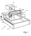
- the laser system 11 comprises a laser arrangement with a laser device 13, in particular a CO 2 laser, which generates an electromagnetic radiation, in particular a laser beam 14.
- the wavelength of the laser beam is preferably in the far infrared range.
- a beam telescope 16 is provided, via which the laser beam 14 generated in the laser device 13 is coupled out. From the beam telescope 16 to the processing point 17, the laser beam 14 is guided by an external optics 18.
- the external optics 18 is provided on a machine base frame 19, which is designed as single or multi-axis depending on the applications. In the present embodiment, the external optic 18 is moved in an X, Y and Z direction. A single or multi-axis optics is also referred to as flying optics. Alternatively, the workpiece and / or the optics may be moved.
- This laser system 11 has a multiplicity of optical elements 23.
- optical elements 23 are also called internal referred to optical elements and include, for example, rearview mirror, Auskoppelapt, Deflection mirror and partially transmitting mirror as well as transmitting Optics such as lenses, which are not shown in detail.
- the external optics 18 has at least a first deflection mirror for beam guidance and beam shaping 23 'and in the processing head 24 at least one further deflection mirror 23' and a focusing optics 23 ", which is designed as a lens, for example the further deflecting mirror 23 'and the focusing optics 23 "can also be a concave mirror be provided.
- the beam path of the laser beam 14 from the beam telescope 16 to the focusing optics 23 " is kept closed by a bellows.
- optical elements 23 have, as shown in Figures 2 to 6, a Support material 31 of metallic material, an alloy or semiconductor material on. In most cases, these optical elements 23 are made of copper or Silicon, wherein the support material 31 is not limited thereto. On the carrier material 31, a coating 32 is provided. This coating 32 can different metals or metal alloys as well as semiconductor materials. Likewise, a multi-layer coating of various types provided his. In the embodiment according to FIGS. 2 to 6, for example, a Support material 31 provided of silicon and a multilayer coating of a layer structure, alternately consisting of a zinc selenide layer and a ThF4 layer. Other assembly and material combinations for the optical elements 23 are possible in many variations.
- FIG. 2 schematically shows a first arrangement for detecting an electrical current Resistance for an optical element 23 shown.
- Contact elements 37 are provided, which via a line 38 information lead to a measuring device 39.
- the contact elements 37 are on the carrier material 31 bonded.
- the contact elements 37 glued, soldered or mechanically clamped.
- it can also be provided that sprung contact pins with a claranpreßkraft to the substrate 31 abut.
- the contact elements 37, the measuring device 39 and the between them lying line 38 form the inventive device 41.
- This device 41 may additionally comprise an evaluation unit 42.
- this Evaluation unit 42 may also be provided in a control of the laser system 11.
- the measuring device 39 detects an electrical resistance, which depends on the temperature due to the laser beam in the optical element 23 absorbed heat changes.
- the contact elements 37 are arranged such that their connecting line 43 intersects the beam axis of the laser beam.
- the contact elements 37 can in the edge region as shown on the substrate 31 may be arranged or on the radial lateral surface. It can also be provided that the coating 32 recesses for receiving and arrangement the contact elements 37 has. Alternatively, the measurement can also be on the coating 32 done.
- one or more connecting wires are provided, which are opposite to the Coating 32 are preferably isolated. This can be a small change the temperature can be detected and recognized immediately.
- an arrangement of the contact elements 37 is provided a coating 32 shown.
- the coating 32 is shown greatly enlarged.
- different levels of conductive are used Layered actual values queried.
- the pair of contact elements 37 ' is, for example connected to the upper conductive layer 33 at the contact surfaces 45.
- the second pair of contact elements 37 is on an underlying electrically conductive Layer 46 arranged.
- the second pair of contact elements 37 may also be arranged on the carrier material 31.
- the multilayer coating is configured such that a pair of contact elements 37 'separated from a second pair of contact elements 37 "on each of an electrically conductive layer 33, 46 is provided, which are separated by a non-conductive layer 25. With multiple conductive layers, at least one or more levels may be used one or more contact elements 37 may be provided.
- FIG. 6 shows an alternative arrangement of the contact elements 37.
- the arranged between the pairs of opposing contact elements 37 Lines 47 represent a schematic grid-shaped division of the measuring field This can be due to the individual detection an approximate temperature profile the surface or measuring plane of the optical element 23 detected and, for example, the incident surface of the laser beam is sufficiently determined become.
- the contact elements 37 may be provided that, for example a lattice structure of thin conductive material on or in the coating 32 or the carrier material 31 is provided. This can also be due to the temperature change, a change in the electrical resistance can be detected.
- the optical element 23 shown in FIG. 2 and the device 41 according to the invention attached thereto have been chosen to produce the diagram shown in FIG. 7 in order to demonstrate the proportionality of the laser power to the change in the magnitude of the electrical resistance.
- the electrical resistance at time t 1 was determined. This value and the other detected values of the electrical resistance are represented by the characteristic curve A.
- the optical element 23 is acted upon by a laser power according to characteristic curve B of, for example, 3,400 W. After a certain period of time, for example between 20 and 100 s, the detectable electrical resistance is almost constant.
- the electrical resistance is reduced by an amount ⁇ R 1 with respect to the initial value or the reference value.
- the laser power was halved, wherein the subsequently detectable electrical resistance corresponds in magnitude to the change in the laser power.
- the absolute change ⁇ R 1 was halved to ⁇ R 2 , as the characteristic A shows at time t 4 .
- the change in the electrical resistance is an example, for example, proportional to the change in power.
- the conditions are generally determined as a function of the carrier material 31 and the coating 32 used and of the location of use of the optical elements 23.
- the determined electrical resistance at time t 5 returns to its initial value at time t 1 .
- the heat generated by the absorbed radiation is in the optical Element 23 in the embodiment proportional to the laser power and the amount Change of the detected electrical resistance a size which with regard to incipient pollution, aging or destruction Classification allows.
Landscapes
- Physics & Mathematics (AREA)
- Engineering & Computer Science (AREA)
- Optics & Photonics (AREA)
- General Physics & Mathematics (AREA)
- Chemical & Material Sciences (AREA)
- Analytical Chemistry (AREA)
- Plasma & Fusion (AREA)
- Mechanical Engineering (AREA)
- Combustion & Propulsion (AREA)
- Lasers (AREA)
- Photometry And Measurement Of Optical Pulse Characteristics (AREA)
- Semiconductor Lasers (AREA)
- Optical Communication System (AREA)
Abstract
Description
- Figur 1
- einen schematischen Aufbau einer Laserbearbeitungsmaschine,
- Figur 2
- eine schematische Darstellung einer Anordnung von Kontaktelementen am Trägermaterial eines optischen Elementes zur Erfassung von Informationen,
- Figur 3
- eine schematische Seitenansicht der Figur 2,
- Figur 4
- eine schematische Darstellung einer alternativen Anordnung von Kontaktelementen an einer Beschichtung des optischen Elementes zur Erfassung von Informationen,
- Figur 5
- eine schematische Seitenansicht der Figur 4,
- Figur 6
- eine schematische Darstellung einer weiteren alternativen Anordnung und
- Figur 7
- ein Diagramm einer Messung eines elektrischen Widerstands von einem optischen Element bei Beaufschlagung mit unterschiedlicher Laserleistung.
Claims (18)
- Verfahren zur Erfassung von Informationen an zumindest einem optischen Element für die Überwachung einer Anlage (11), bei der eine elektromagnetische Strahlung von dem zumindest einen optischen Element (23) geformt oder geführt wird, insbesondere zur Überwachung einer Laseranordnung, bei dem eine Änderung zumindest einer physikalischen Größe in oder an dem zumindest einen optischen Element (23) durch die absorbierte elektromagnetische Strahlung mit einer Meßeinreichung (39) erfaßt wird, bei dem zumindest ein durch die Meßeinrichtung (39) erfaßter Ist-Wert an eine Auswerteeinheit (42) weitergeleitet wird und bei dem der zumindest eine Ist-Wert mit einem in der Auswerteeinheit (42) hinterlegten Referenzwert verglichen wird.
- Verfahren nach Anspruch 1, dadurch gekennzeichnet, daß die durch die Absorption der elektromagnetischen Strahlung erzeugte Änderung in dem optischen Element (23) mit der Meßeinrichtung (39) durch eine elektrische Widerstandsmessung erfaßt wird.
- Verfahren nach Anspruch 1, dadurch gekennzeichnet, daß die durch die Absorption der elektromagnetischen Strahlung erzeugte Änderung in dem optischen Element (23) mit der Meßeinrichtung (39) durch eine kapazitive Messung erfaßt wird.
- Verfahren nach einem der Ansprüche 1 bis 3, dadurch gekennzeichnet, daß der Referenzwert und der beziehungsweise die Ist-Werte an einem Trägermaterial (31) des optischen Elementes (23) erfaßt werden.
- Verfahren nach Anspruch 1 bis 3, dadurch gekennzeichnet, daß der Referenzwert und der beziehungsweise die Ist-Werte an einer Beschichtung (32) auf dem Trägermaterial (31) eines optischen Elementes (23) erfaßt werden.
- Verfahren nach einem der vorhergehenden Ansprüche, dadurch gekennzeichnet, daß der Ist-Wert zeitverzögert nach dem erstmaligen Auftreffen von elektromagnetischer Strahlung auf das optische Element (23) erfaßt wird.
- Verfahren nach einem der vorhergehenden Ansprüche, dadurch gekennzeichnet, daß für jedes optische Element ein Referenzwert, vorzugsweise bei Betriebstemperatur, vor dem Einbau oder vor der Inbetriebnahme in einer Laseranordnung (11) erfaßt wird.
- Verfahren nach einem der vorhergehenden Ansprüche, dadurch gekennzeichnet, daß die Änderung einer Leistung des elektromagnetischen Strahles als Änderung der physikalischen Größe, vorzugsweise als Änderung des elektrischen Widerstandes, erfaßt wird und beim Überschreiten oder Unterschreiten eines zum Referenzwert wählbaren oberen oder unteren Grenzwertes der Leistung ein Signal zur Warnung, Nachregelung oder Abschaltung der Anlage, insbesondere der Laseranordnung, von einer Auswerteeinheit (42) ausgegeben wird.
- Verfahren nach einem der vorhergehenden Ansprüche, dadurch gekennzeichnet, daß zur Überwachung der Leistung des elektromagnetischen Strahls von zumindest zwei, vorzugsweise jedem optischen Element (23), Ist-Werte der Meßeinrichtung (39) während des Betriebes der Anlage (11) erfaßt werden, diese Ist-Werte mit einem gemeinsamen Referenzwert für alle optischen Elemente (23) oder dem jeweiligen optischen Element (23) zugeordneten Referenzwert in der Auswerteeinheit (42) verglichen werden, eine betragsmäßige Abweichung ermittelt und einer entsprechenden Leistung des elektromagnetischen Strahls gleichgesetzt wird und vorzugsweise im Laserresonator einer Laseranlage die erzeugte Laserleistung durch einen thermischen Absorber erfaßt wird, welcher mit dem oder den an den optischen Elementen (23) erfaßten Laserleistungen verglichen wird.
- Verfahren nach einem der vorhergehenden Ansprüche, dadurch gekennzeichnet, daß die Ermittlung der Ist-Werte in einen Online-Prozeß integriert und dauerhaft in frei wählbaren oder festgelegten Zeitintervallen erfaßt werden.
- Verfahren nach einem der vorhergehenden Ansprüche, dadurch gekennzeichnet, daß eine Schar von Kennlinien über unterschiedliche Zustände der optischen Elemente (23) ermittelt wird, daß diese Schar von Kennlinien in einer Auswerteeinheit (42) gespeichert wird und zur Auswertung der tatsächlichen Zustände der optischen Elemente (23) mit dem beziehungsweise den Ist-Werten verglichen werden.
- Vorrichtung zur Erfassung von Informationen an zumindest einem optischen Element (23) für die Überwachung einer Anlage (11), insbesondere zur Durchführung des Verfahrens, dadurch gekennzeichnet, daß eine Meßeinrichtung (39) zumindest ein Kontaktelement (37) aufweist, welches an zumindest einem optischen Element (23) anordenbar ist und daß die Meßeinrichtung (39) Meßsignale an eine Auswerteeinheit (42) übermittelt.
- Vorrichtung nach Anspruch 12, dadurch gekennzeichnet, daß zwei einander zugeordnete Kontaktelemente (37) vorgesehen sind, welche entfernt von einer Strahlachse eines elektromagnetischen Strahles, insbesondere eines Laserstrahls, an dem optischen Element (23) vorgesehen sind.
- Vorrichtung nach Anspruch 12 oder 13, dadurch gekennzeichnet, daß das zumindest eine Kontaktelement (37) an einem Trägermaterial (31) oder einer Beschichtung (32) auf dem Trägermaterial (31) des optischen Elements (23) lösbar, vorzugsweise durch eine mechanische Verbindung oder durch unter Druck beanspruchte Kontaktelemente, oder fest, vorzugsweise durch Kleben, Löten, Schweißen, Bonden, vorgesehen ist.
- Vorrichtung nach einem der Ansprüche 12 bis 14, dadurch gekennzeichnet, daß bei einer Multilayerbeschichtung an zumindest einer, vorzugsweise elektrisch leitfähigen Schicht zumindest zwei Kontaktelemente (37) zur Bildung einer Meßebene angeordnet sind.
- Vorrichtung nach einem der Ansprüche 12 bis 15, dadurch gekennzeichnet, daß an einem optischen Element (23) mehrere Kontaktelemente (37) vorgesehen sind, die paarweise entfernt zueinander angeordnet sind und daß die zwischen den Kontaktelementen (37) gebildeten Geraden parallel oder in einem beliebigen Winkel zueinander verlaufen.
- Vorrichtung nach einem der Ansprüche 12 bis 16, dadurch gekennzeichnet, daß auf oder in dem optischen Element (23) leitende Drähte oder zumindest eine Gitterstruktur vorgesehen ist, welche entfernt von der Strahlachse der elektromagnetischen Strahlung mit dem zumindest einen Kontaktelement (37) verbindbar sind.
- Vorrichtung nach einem der Ansprüche 12 bis 17, dadurch gekennzeichnet, daß die optischen Elemente (23) in einer Laseranordnung, welche vorzugsweise einen CO2-Laser aufweist, vorgesehen sind und die Laserleistung eines Laserstrahles als auch eine Veränderung der optischen Elemente (23) erfaßbar ist.
Priority Applications (4)
| Application Number | Priority Date | Filing Date | Title |
|---|---|---|---|
| DE50110761T DE50110761D1 (de) | 2001-11-09 | 2001-11-09 | Verfahren und Vorrichtung zur Erfassung von Informationen für die Überwachung einer Laseranordnung |
| EP01126740A EP1310782B1 (de) | 2001-11-09 | 2001-11-09 | Verfahren und Vorrichtung zur Erfassung von Informationen für die Überwachung einer Laseranordnung |
| AT01126740T ATE336708T1 (de) | 2001-11-09 | 2001-11-09 | Verfahren und vorrichtung zur erfassung von informationen für die überwachung einer laseranordnung |
| US10/288,093 US6934017B2 (en) | 2001-11-09 | 2002-11-04 | Method and device for detection of information on optical elements, particularly for monitoring a laser arrangement |
Applications Claiming Priority (1)
| Application Number | Priority Date | Filing Date | Title |
|---|---|---|---|
| EP01126740A EP1310782B1 (de) | 2001-11-09 | 2001-11-09 | Verfahren und Vorrichtung zur Erfassung von Informationen für die Überwachung einer Laseranordnung |
Publications (2)
| Publication Number | Publication Date |
|---|---|
| EP1310782A1 true EP1310782A1 (de) | 2003-05-14 |
| EP1310782B1 EP1310782B1 (de) | 2006-08-16 |
Family
ID=8179202
Family Applications (1)
| Application Number | Title | Priority Date | Filing Date |
|---|---|---|---|
| EP01126740A Expired - Lifetime EP1310782B1 (de) | 2001-11-09 | 2001-11-09 | Verfahren und Vorrichtung zur Erfassung von Informationen für die Überwachung einer Laseranordnung |
Country Status (4)
| Country | Link |
|---|---|
| US (1) | US6934017B2 (de) |
| EP (1) | EP1310782B1 (de) |
| AT (1) | ATE336708T1 (de) |
| DE (1) | DE50110761D1 (de) |
Cited By (5)
| Publication number | Priority date | Publication date | Assignee | Title |
|---|---|---|---|---|
| WO2006103104A1 (de) * | 2005-04-01 | 2006-10-05 | Trumpf Werkzeugmaschinen Gmbh + Co. Kg | Optisches element sowie verfahren zur erfassung von strahlparametern, mit einem als pixels-matrix ausgebildeten temperatursensor |
| EP1728582A1 (de) | 2005-05-31 | 2006-12-06 | Trumpf Laser- und Systemtechnik GmbH | Einrichtung zur Erfassung von Veränderungen eines Laserstrahls |
| WO2007073744A1 (de) * | 2005-12-15 | 2007-07-05 | Trumpf Werkzeugmaschinen Gmbh + Co. Kg | Verfahren zur zustandserkennung eines optischen elements |
| DE102016123000B3 (de) * | 2016-11-29 | 2017-12-14 | Scansonic Mi Gmbh | Verfahren zur Überwachung eines Schutzglases und Überwachungsvorrichtung |
| DE102018102828A1 (de) | 2018-02-08 | 2019-08-08 | Scansonic Mi Gmbh | Verfahren zur Überwachung eines Schutzglases |
Families Citing this family (7)
| Publication number | Priority date | Publication date | Assignee | Title |
|---|---|---|---|---|
| US7800079B2 (en) * | 2003-12-22 | 2010-09-21 | Asml Netherlands B.V. | Assembly for detection of radiation flux and contamination of an optical component, lithographic apparatus including such an assembly and device manufacturing method |
| US7897110B2 (en) * | 2005-12-20 | 2011-03-01 | Asml Netherlands B.V. | System and method for detecting at least one contamination species in a lithographic apparatus |
| US7641152B2 (en) * | 2007-04-13 | 2010-01-05 | The Boeing Company | Dynamic adjustment of wing surfaces for variable camber |
| JP2016010809A (ja) * | 2014-06-30 | 2016-01-21 | 株式会社ディスコ | レーザー加工装置 |
| CN106053021B (zh) * | 2016-05-18 | 2018-07-20 | 东南大学 | 一种分布反馈式激光器时频响应曲线的确定方法 |
| FR3103033A1 (fr) * | 2019-11-07 | 2021-05-14 | Stmicroelectronics Sa | État d'un système optique |
| CN113340565B (zh) * | 2021-05-07 | 2023-11-07 | 桂林芯隆科技有限公司 | 一种用于激光器单条端面检测的放置夹具 |
Citations (4)
| Publication number | Priority date | Publication date | Assignee | Title |
|---|---|---|---|---|
| JPS62139374A (ja) * | 1985-12-13 | 1987-06-23 | Matsushita Electric Ind Co Ltd | レ−ザ装置 |
| US4692623A (en) * | 1986-02-13 | 1987-09-08 | The United States Of America As Represented By The Secretary Of The Army | Precision laser beam positioner and spatially resolved laser beam sampling meter |
| FR2698495A1 (fr) * | 1992-11-23 | 1994-05-27 | Aerospatiale | Dispositif de contrôle de l'état de la lentille de focalisation d'un appareil laser et appareil laser utilisant ce dispositif. |
| DE10007976C1 (de) * | 2000-02-22 | 2001-09-06 | Precitec Gmbh | Laserbearbeitungskopf und Verfahren zum Messen der Temperatur seiner Linsenanordnung |
Family Cites Families (8)
| Publication number | Priority date | Publication date | Assignee | Title |
|---|---|---|---|---|
| DE1918760U (de) * | 1965-02-23 | 1965-07-01 | Deutsche Bundespost | Kontaktklemme. |
| US4283378A (en) * | 1979-08-01 | 1981-08-11 | Cabot Corporation | Production of high surface area carbon blacks |
| US5478456A (en) * | 1993-10-01 | 1995-12-26 | Minnesota Mining And Manufacturing Company | Sputtering target |
| CH690796A5 (de) * | 1994-12-20 | 2001-01-15 | Bystronic Laser Ag | Anordnung zur Messung von Kenngrössen eines Laserstrahls mit einem Spiegel. |
| DE19636249C2 (de) * | 1996-08-28 | 1999-06-24 | Tu Berlin Optisches Inst Sekre | Anordnung zum Schutz von optischen Komponenten |
| DE50001492D1 (de) * | 2000-05-15 | 2003-04-24 | Prometec Gmbh | Verfahren und Vorrichtung zum Überwachen des Verschleisszustandes eines Werkzeuges |
| US6528762B2 (en) * | 2001-02-12 | 2003-03-04 | W. A. Whitney Co. | Laser beam position control apparatus for a CNC laser equipped machine tool |
| DE10108955C2 (de) * | 2001-02-23 | 2003-04-17 | Precitec Kg | Verfahren zum Ermitteln des Verschleissgrades einer Linsenanordnung in einem Laserbearbeitungskopf sowie Laserbearbeitungskopf |
-
2001
- 2001-11-09 DE DE50110761T patent/DE50110761D1/de not_active Expired - Lifetime
- 2001-11-09 EP EP01126740A patent/EP1310782B1/de not_active Expired - Lifetime
- 2001-11-09 AT AT01126740T patent/ATE336708T1/de not_active IP Right Cessation
-
2002
- 2002-11-04 US US10/288,093 patent/US6934017B2/en not_active Expired - Lifetime
Patent Citations (4)
| Publication number | Priority date | Publication date | Assignee | Title |
|---|---|---|---|---|
| JPS62139374A (ja) * | 1985-12-13 | 1987-06-23 | Matsushita Electric Ind Co Ltd | レ−ザ装置 |
| US4692623A (en) * | 1986-02-13 | 1987-09-08 | The United States Of America As Represented By The Secretary Of The Army | Precision laser beam positioner and spatially resolved laser beam sampling meter |
| FR2698495A1 (fr) * | 1992-11-23 | 1994-05-27 | Aerospatiale | Dispositif de contrôle de l'état de la lentille de focalisation d'un appareil laser et appareil laser utilisant ce dispositif. |
| DE10007976C1 (de) * | 2000-02-22 | 2001-09-06 | Precitec Gmbh | Laserbearbeitungskopf und Verfahren zum Messen der Temperatur seiner Linsenanordnung |
Non-Patent Citations (2)
| Title |
|---|
| PATENT ABSTRACTS OF JAPAN vol. 011, no. 367 (E - 561) 28 November 1987 (1987-11-28) * |
| PROMETEC GMBH: "In-Process-Messung und Überwachung von unfokussierter Laserstrahlung - Laserscope UFC 60", -, 11 January 2001 (2001-01-11), XP002197030, Retrieved from the Internet <URL:http://www.prometec.de/german/pages/framesets/laser_diagnostics.htm> [retrieved on 20020416] * |
Cited By (8)
| Publication number | Priority date | Publication date | Assignee | Title |
|---|---|---|---|---|
| WO2006103104A1 (de) * | 2005-04-01 | 2006-10-05 | Trumpf Werkzeugmaschinen Gmbh + Co. Kg | Optisches element sowie verfahren zur erfassung von strahlparametern, mit einem als pixels-matrix ausgebildeten temperatursensor |
| EP1728582A1 (de) | 2005-05-31 | 2006-12-06 | Trumpf Laser- und Systemtechnik GmbH | Einrichtung zur Erfassung von Veränderungen eines Laserstrahls |
| WO2006128671A1 (de) | 2005-05-31 | 2006-12-07 | Trumpf Laser- Und Systemtechnik Gmbh | Laserbearbeitungsmaschine mit einer einrichtung zur erfassung von veränderungen des laserstrahls |
| WO2007073744A1 (de) * | 2005-12-15 | 2007-07-05 | Trumpf Werkzeugmaschinen Gmbh + Co. Kg | Verfahren zur zustandserkennung eines optischen elements |
| US7705292B2 (en) | 2005-12-15 | 2010-04-27 | Trumpf Werkzeugmaschinen Gmbh + Co. Kg | Method and apparatus for detecting a condition of an optical element |
| CN101341000B (zh) * | 2005-12-15 | 2011-08-24 | 通快机床两合公司 | 用于激光装置的光学元件的状态识别的方法以及激光装置 |
| DE102016123000B3 (de) * | 2016-11-29 | 2017-12-14 | Scansonic Mi Gmbh | Verfahren zur Überwachung eines Schutzglases und Überwachungsvorrichtung |
| DE102018102828A1 (de) | 2018-02-08 | 2019-08-08 | Scansonic Mi Gmbh | Verfahren zur Überwachung eines Schutzglases |
Also Published As
| Publication number | Publication date |
|---|---|
| DE50110761D1 (de) | 2006-09-28 |
| EP1310782B1 (de) | 2006-08-16 |
| ATE336708T1 (de) | 2006-09-15 |
| US20030090256A1 (en) | 2003-05-15 |
| US6934017B2 (en) | 2005-08-23 |
Similar Documents
| Publication | Publication Date | Title |
|---|---|---|
| EP0414869B1 (de) | Verfahren zur qualitätssicherung beim laserstrahlschweissen und -schneiden | |
| EP3521810B1 (de) | Analysegerät zur bestimmung von feinstaub | |
| DE10338256B4 (de) | Teilchenzähler mit Streifenlaserdiode | |
| EP1888293B1 (de) | Optisches element sowie verfahren zur erfassung von strahlparametern, mit einem als pixels-matrix ausgebildeten temperatursensor | |
| DE10113518B4 (de) | Verfahren zur Messung des Verschmutzungsgrades eines Schutzglases eines Laserbearbeitungskopfs sowie Laserbearbeitungsanlage zur Durchführung des Verfahrens | |
| DE102018102828B4 (de) | Verfahren zur Überwachung eines Schutzglases | |
| EP1310782B1 (de) | Verfahren und Vorrichtung zur Erfassung von Informationen für die Überwachung einer Laseranordnung | |
| EP2361714B1 (de) | Verfahren und Anordnung zum Laserlöten | |
| EP2516101B1 (de) | Verfahren und vorrichtung zur erfassung und justierung des fokus eines laserstrahls bei der laserbearbeitung von werkstücken | |
| EP1128927A1 (de) | Verfahren und vorrichtung zum bearbeiten von werkstücken mit hochenergiestrahlung | |
| DE102010015023B4 (de) | Verfahren und Vorrichtung zur Qualitätssicherung und Prozesskontrolle bei der Laserbearbeitung von Werkstücken | |
| EP2059365A1 (de) | Überwachungsvorrichtung für eine laserbearbeitungsvorrichtung | |
| DE102017115922C5 (de) | Verfahren und Vorrichtung zur Messung und Einstellung eines Abstands zwischen einem Bearbeitungskopf und einem Werkstück sowie dazugehöriges Verfahren zur Regelung | |
| EP1693141A2 (de) | Anordnung und Verfahren zur ortsaufgelösten Temperaturmessung bei einem Laserbearbeitungsverfahren | |
| EP4106945A1 (de) | VERFAHREN ZUM ANALYSIEREN EINER SCHWEIßVERBINDUNG BEIM LASERSCHWEIßEN VON WERKSTÜCKEN | |
| EP0252268A2 (de) | Verfahren zur Überwachung des Bearbeitungsprozesses mit einer Hochleistungsenergiequelle, insbesondere einem Laser, und Bearbeitungsoptik zur Durchführung desselben | |
| DE102015103887A1 (de) | Laserbearbeitungsvorrichtung mit einer Funktion zur Überwachung der Ausbreitung eines Laserstrahls | |
| EP2999568B1 (de) | Laserbearbeitungsdüse für eine laserbearbeitungseinrichtung und laserbearbeitungseinrichtung | |
| DE19516376C2 (de) | Verfahren und Vorrichtung zur Kontrolle und Regelung der Brennfleckposition bei der Lasermaterialbearbeitung | |
| EP2015888A1 (de) | Laserbearbeitungsmaschine und laserbearbeitungsverfahren | |
| DE102021101658B4 (de) | Laserbearbeitungskopf mit chromatischer Kompensationsvorrichtung | |
| WO2022029073A1 (de) | Verfahren zum bestimmen einer position eines werkstücks für einen laserbearbeitungsprozess und laserbearbeitungssystem | |
| WO2002103307A1 (de) | Verfahren und vorrichtung zur diagnostik und überwachung eines unfokussierten laserstrahles von hochleistungs-laseranlagen | |
| DE4006618C2 (de) | Vorrichtung zur Auskoppelung einer Meßstrahlung aus einem Laserstrahl | |
| DE102018211832A1 (de) | Verfahren sowie eine Vorrichtung zur Messung und Regelung eines Energieaufnahmepotentials in der Interaktionszone eines Beleuchtungsstrahls mit einem Pulvergasstrahl |
Legal Events
| Date | Code | Title | Description |
|---|---|---|---|
| PUAI | Public reference made under article 153(3) epc to a published international application that has entered the european phase |
Free format text: ORIGINAL CODE: 0009012 |
|
| 17P | Request for examination filed |
Effective date: 20011109 |
|
| AK | Designated contracting states |
Designated state(s): AT BE CH CY DE DK ES FI FR GB GR IE IT LI LU MC NL PT SE TR |
|
| AX | Request for extension of the european patent |
Extension state: AL LT LV MK RO SI |
|
| AKX | Designation fees paid |
Designated state(s): AT BE CH CY DE DK ES FI FR GB GR IE IT LI LU MC NL PT SE TR |
|
| 17Q | First examination report despatched |
Effective date: 20040421 |
|
| GRAP | Despatch of communication of intention to grant a patent |
Free format text: ORIGINAL CODE: EPIDOSNIGR1 |
|
| GRAS | Grant fee paid |
Free format text: ORIGINAL CODE: EPIDOSNIGR3 |
|
| GRAA | (expected) grant |
Free format text: ORIGINAL CODE: 0009210 |
|
| RIN1 | Information on inventor provided before grant (corrected) |
Inventor name: KIRCHER, STEFFEN |
|
| AK | Designated contracting states |
Kind code of ref document: B1 Designated state(s): AT BE CH CY DE DK ES FI FR GB GR IE IT LI LU MC NL PT SE TR |
|
| PG25 | Lapsed in a contracting state [announced via postgrant information from national office to epo] |
Ref country code: IT Free format text: LAPSE BECAUSE OF FAILURE TO SUBMIT A TRANSLATION OF THE DESCRIPTION OR TO PAY THE FEE WITHIN THE PRE;WARNING: LAPSES OF ITALIAN PATENTS WITH EFFECTIVE DATE BEFORE 2007 MAY HAVE OCCURRED AT ANY TIME BEFORE 2007. THE CORRECT EFFECTIVE DATE MAY BE DIFFERENT FROM THE ONE RECORDED.SCRIBED TIME-LIMIT Effective date: 20060816 Ref country code: NL Free format text: LAPSE BECAUSE OF FAILURE TO SUBMIT A TRANSLATION OF THE DESCRIPTION OR TO PAY THE FEE WITHIN THE PRESCRIBED TIME-LIMIT Effective date: 20060816 Ref country code: FI Free format text: LAPSE BECAUSE OF FAILURE TO SUBMIT A TRANSLATION OF THE DESCRIPTION OR TO PAY THE FEE WITHIN THE PRESCRIBED TIME-LIMIT Effective date: 20060816 Ref country code: IE Free format text: LAPSE BECAUSE OF FAILURE TO SUBMIT A TRANSLATION OF THE DESCRIPTION OR TO PAY THE FEE WITHIN THE PRESCRIBED TIME-LIMIT Effective date: 20060816 |
|
| REG | Reference to a national code |
Ref country code: GB Ref legal event code: FG4D Free format text: NOT ENGLISH |
|
| REG | Reference to a national code |
Ref country code: CH Ref legal event code: EP |
|
| REG | Reference to a national code |
Ref country code: IE Ref legal event code: FG4D Free format text: LANGUAGE OF EP DOCUMENT: GERMAN |
|
| REF | Corresponds to: |
Ref document number: 50110761 Country of ref document: DE Date of ref document: 20060928 Kind code of ref document: P |
|
| REG | Reference to a national code |
Ref country code: CH Ref legal event code: NV Representative=s name: E. BLUM & CO. PATENTANWAELTE |
|
| PG25 | Lapsed in a contracting state [announced via postgrant information from national office to epo] |
Ref country code: SE Free format text: LAPSE BECAUSE OF FAILURE TO SUBMIT A TRANSLATION OF THE DESCRIPTION OR TO PAY THE FEE WITHIN THE PRESCRIBED TIME-LIMIT Effective date: 20061116 Ref country code: DK Free format text: LAPSE BECAUSE OF FAILURE TO SUBMIT A TRANSLATION OF THE DESCRIPTION OR TO PAY THE FEE WITHIN THE PRESCRIBED TIME-LIMIT Effective date: 20061116 |
|
| PG25 | Lapsed in a contracting state [announced via postgrant information from national office to epo] |
Ref country code: ES Free format text: LAPSE BECAUSE OF FAILURE TO SUBMIT A TRANSLATION OF THE DESCRIPTION OR TO PAY THE FEE WITHIN THE PRESCRIBED TIME-LIMIT Effective date: 20061127 |
|
| PG25 | Lapsed in a contracting state [announced via postgrant information from national office to epo] |
Ref country code: BE Free format text: LAPSE BECAUSE OF NON-PAYMENT OF DUE FEES Effective date: 20061130 Ref country code: MC Free format text: LAPSE BECAUSE OF NON-PAYMENT OF DUE FEES Effective date: 20061130 |
|
| GBT | Gb: translation of ep patent filed (gb section 77(6)(a)/1977) |
Effective date: 20061122 |
|
| PG25 | Lapsed in a contracting state [announced via postgrant information from national office to epo] |
Ref country code: PT Free format text: LAPSE BECAUSE OF FAILURE TO SUBMIT A TRANSLATION OF THE DESCRIPTION OR TO PAY THE FEE WITHIN THE PRESCRIBED TIME-LIMIT Effective date: 20070116 |
|
| NLV1 | Nl: lapsed or annulled due to failure to fulfill the requirements of art. 29p and 29m of the patents act | ||
| REG | Reference to a national code |
Ref country code: IE Ref legal event code: FD4D |
|
| EN | Fr: translation not filed | ||
| PLBE | No opposition filed within time limit |
Free format text: ORIGINAL CODE: 0009261 |
|
| STAA | Information on the status of an ep patent application or granted ep patent |
Free format text: STATUS: NO OPPOSITION FILED WITHIN TIME LIMIT |
|
| 26N | No opposition filed |
Effective date: 20070518 |
|
| REG | Reference to a national code |
Ref country code: CH Ref legal event code: PFA Owner name: TRUMPF WERKZEUGMASCHINEN GMBH + CO. KG Free format text: TRUMPF WERKZEUGMASCHINEN GMBH + CO. KG#JOHANN-MAUS-STRASSE 2#71254 DITZINGEN (DE) -TRANSFER TO- TRUMPF WERKZEUGMASCHINEN GMBH + CO. KG#JOHANN-MAUS-STRASSE 2#71254 DITZINGEN (DE) |
|
| BERE | Be: lapsed |
Owner name: TRUMPF WERKZEUGMASCHINEN G.M.B.H. + CO. KG Effective date: 20061130 |
|
| PG25 | Lapsed in a contracting state [announced via postgrant information from national office to epo] |
Ref country code: GR Free format text: LAPSE BECAUSE OF FAILURE TO SUBMIT A TRANSLATION OF THE DESCRIPTION OR TO PAY THE FEE WITHIN THE PRESCRIBED TIME-LIMIT Effective date: 20061117 Ref country code: FR Free format text: LAPSE BECAUSE OF FAILURE TO SUBMIT A TRANSLATION OF THE DESCRIPTION OR TO PAY THE FEE WITHIN THE PRESCRIBED TIME-LIMIT Effective date: 20070511 |
|
| PG25 | Lapsed in a contracting state [announced via postgrant information from national office to epo] |
Ref country code: TR Free format text: LAPSE BECAUSE OF FAILURE TO SUBMIT A TRANSLATION OF THE DESCRIPTION OR TO PAY THE FEE WITHIN THE PRESCRIBED TIME-LIMIT Effective date: 20060816 Ref country code: LU Free format text: LAPSE BECAUSE OF NON-PAYMENT OF DUE FEES Effective date: 20061109 |
|
| PG25 | Lapsed in a contracting state [announced via postgrant information from national office to epo] |
Ref country code: FR Free format text: LAPSE BECAUSE OF FAILURE TO SUBMIT A TRANSLATION OF THE DESCRIPTION OR TO PAY THE FEE WITHIN THE PRESCRIBED TIME-LIMIT Effective date: 20060816 Ref country code: CY Free format text: LAPSE BECAUSE OF FAILURE TO SUBMIT A TRANSLATION OF THE DESCRIPTION OR TO PAY THE FEE WITHIN THE PRESCRIBED TIME-LIMIT Effective date: 20060816 |
|
| PGFP | Annual fee paid to national office [announced via postgrant information from national office to epo] |
Ref country code: CH Payment date: 20081124 Year of fee payment: 8 |
|
| PGFP | Annual fee paid to national office [announced via postgrant information from national office to epo] |
Ref country code: AT Payment date: 20081120 Year of fee payment: 8 |
|
| PGFP | Annual fee paid to national office [announced via postgrant information from national office to epo] |
Ref country code: IT Payment date: 20081125 Year of fee payment: 8 |
|
| PGFP | Annual fee paid to national office [announced via postgrant information from national office to epo] |
Ref country code: GB Payment date: 20081121 Year of fee payment: 8 |
|
| REG | Reference to a national code |
Ref country code: CH Ref legal event code: PL |
|
| GBPC | Gb: european patent ceased through non-payment of renewal fee |
Effective date: 20091109 |
|
| PG25 | Lapsed in a contracting state [announced via postgrant information from national office to epo] |
Ref country code: AT Free format text: LAPSE BECAUSE OF NON-PAYMENT OF DUE FEES Effective date: 20091109 |
|
| PG25 | Lapsed in a contracting state [announced via postgrant information from national office to epo] |
Ref country code: LI Free format text: LAPSE BECAUSE OF NON-PAYMENT OF DUE FEES Effective date: 20091130 Ref country code: CH Free format text: LAPSE BECAUSE OF NON-PAYMENT OF DUE FEES Effective date: 20091130 |
|
| PG25 | Lapsed in a contracting state [announced via postgrant information from national office to epo] |
Ref country code: GB Free format text: LAPSE BECAUSE OF NON-PAYMENT OF DUE FEES Effective date: 20091109 |
|
| PG25 | Lapsed in a contracting state [announced via postgrant information from national office to epo] |
Ref country code: IT Free format text: LAPSE BECAUSE OF NON-PAYMENT OF DUE FEES Effective date: 20091109 |
|
| PGFP | Annual fee paid to national office [announced via postgrant information from national office to epo] |
Ref country code: DE Payment date: 20191121 Year of fee payment: 19 |
|
| REG | Reference to a national code |
Ref country code: DE Ref legal event code: R119 Ref document number: 50110761 Country of ref document: DE |
|
| PG25 | Lapsed in a contracting state [announced via postgrant information from national office to epo] |
Ref country code: DE Free format text: LAPSE BECAUSE OF NON-PAYMENT OF DUE FEES Effective date: 20210601 |