EP1309238A2 - Controlling data flow across an RF barrier - Google Patents
Controlling data flow across an RF barrier Download PDFInfo
- Publication number
- EP1309238A2 EP1309238A2 EP02257424A EP02257424A EP1309238A2 EP 1309238 A2 EP1309238 A2 EP 1309238A2 EP 02257424 A EP02257424 A EP 02257424A EP 02257424 A EP02257424 A EP 02257424A EP 1309238 A2 EP1309238 A2 EP 1309238A2
- Authority
- EP
- European Patent Office
- Prior art keywords
- cavity
- electronics
- enclosure
- barrier
- control
- Prior art date
- Legal status (The legal status is an assumption and is not a legal conclusion. Google has not performed a legal analysis and makes no representation as to the accuracy of the status listed.)
- Granted
Links
Images

Classifications
-
- H—ELECTRICITY
- H04—ELECTRIC COMMUNICATION TECHNIQUE
- H04B—TRANSMISSION
- H04B17/00—Monitoring; Testing
-
- G—PHYSICS
- G01—MEASURING; TESTING
- G01R—MEASURING ELECTRIC VARIABLES; MEASURING MAGNETIC VARIABLES
- G01R29/00—Arrangements for measuring or indicating electric quantities not covered by groups G01R19/00 - G01R27/00
- G01R29/08—Measuring electromagnetic field characteristics
- G01R29/0807—Measuring electromagnetic field characteristics characterised by the application
- G01R29/0814—Field measurements related to measuring influence on or from apparatus, components or humans, e.g. in ESD, EMI, EMC, EMP testing, measuring radiation leakage; detecting presence of micro- or radiowave emitters; dosimetry; testing shielding; measurements related to lightning
- G01R29/0821—Field measurements related to measuring influence on or from apparatus, components or humans, e.g. in ESD, EMI, EMC, EMP testing, measuring radiation leakage; detecting presence of micro- or radiowave emitters; dosimetry; testing shielding; measurements related to lightning rooms and test sites therefor, e.g. anechoic chambers, open field sites or TEM cells
Definitions
- This invention relates generally to the field of radio frequency (RF) fixture devices, and more specifically to a method of controlling electronics across an RF barrier, in particular with a serial interface bus.
- RF radio frequency
- RF enclosures may be used in a variety of test and measurement applications when the amount of RF radiation that impacts a device under test (DUT) must be carefully controlled. Specific examples include prototype testing and production testing of cellular telephones, portable computers, pagers, and other small electronic devices. Often RF enclosures are used in automated or semi-automated environments in which machines are used to place the DUT inside the RF enclosure. In these types of test environments, it is desirable to be able to evaluate the functionality and correct operation of the DUT while the DUT is within the RF enclosure.
- the use of electronics circuitry and software may be used to apply specific test resources to the DUT and measure the responses. In most applications, the electronics circuitry and software is located both internal and external to the RF enclosure.
- a further issue when electronics components are used within an RF enclosure is the complexity of the interface between the electronics inside the RF enclosure and the electronics outside the RF enclosure. As the number of communication paths that cross the RF interface increase, so does the amount of RF noise generated by each path. Thus, a secondary design consideration is the method of controlling the electronics path across an RF barrier of an RF enclosure.
- the RF enclosure may be used to test and prototype electronics devices, such as cell phones, personal digital assistants (PDAs), and other similar electronics.
- PDAs personal digital assistants
- Most methods of controlling electronics across an RF barrier use electrical signals propagating through a filtered connector as the primary transport mechanism. These electrical signals can carry data reads and data writes to and from the electronics within an RF enclosure. Most of these methods may be classified into one of three basic types: direct drive, wide parallel, and command serial.
- a direct drive control method consists of providing dedicated electrical resources outside of the RF enclosure that pass through the filtered connector(s) for each element being controlled.
- An example of this type of control method would be to generate relay coil drive signals outside the RF cavity and pass each of these drive lines through the filtered connectors to relays inside the cavity.
- This method requires an individual control line that passes through the filtered connector for each resource being controlled. It is desirable to limit the number of control lines passing through the filtered connectors since these filtered connectors are very expensive (approximately $2.00/line) and the effective RF isolation of the structure degrades with the number of signals passing through the filtered connectors.
- a direct drive scheme is also not very flexible or expandable.
- a wide parallel control method consists of a conventional address, data, and control scheme in which all signals must pass through the filtered connectors(s) to register based electronics inside the RF cavity. This method often requires a large number of signals passing through the filtered connectors.
- a typical implementation might consist of 16 or more lines: 8 data, 5 address, and 3 control.
- Many RF test fixtures such as the TS-50 (Yukon) and the Z2030A (Osprey) use this control method.
- a command serial control method consists of sending commands across the filtered connector(s) to a microprocessor or other programmable logic device that can interpret these commands into control sequences. This method commonly requires a clock to be running at all times inside the RF enclosed portion for clocking the microprocessor or logic device. This clock creates spurious noise that can interfere with the measurements inside the RF cavity. Command serial control methods are also more complicated and often require some firmware programming.
- the present invention takes advantage of the industry standard serial data control buses capable of serially shifting data in and/or out of electronics being controlled in some pre-determined protocol to provide a serial data control protocol for controlling electronics across an RF barrier.
- a microprocessor with a built-in serial data control bus e.g., SPI
- An address dependent form of the serial bus passes through one or more RF filtered connectors into the RF cavity.
- the processor uses the serial data bus to control (data reads and data writes) an arbitrary amount of electronics inside and outside of the RF cavity. This control method requires a minimal number of signals passing through the filtered connectors, preserving the RF isolation of the cavity from the external environment.
- the addressing scheme is designed to specifically isolate electronics outside the RF chamber from the electronics inside the chamber.
- the serial data bus lines that pass through into the RF cavity are held in a quiescent state unless being used to control electronics inside the RF cavity.
- This signal isolation technique provides a very low spurious noise environment inside the RF cavity. This is important for sensitive RF measurements, while allowing the processor to control external electronics.
- This gating functionality may additionally have a temporal aspect that controls when individual signals are gated from entering the RF cavity. This provides the important advantage of being able to selectively control noise levels experienced during the testing process.
- DACs Digital-to-Analog Converters
- ADCs Analog-to-Digital Converters
- the present invention is able to use these serial data control buses to provide a serial data control protocol for controlling electronics across an RF barrier.
- a microprocessor with a built-in serial data control bus e.g., SPI
- An address dependent form of the serial bus passes through one or more RF filtered connectors into the RF cavity.
- the processor uses the serial data bus to control (data reads and data writes) an arbitrary amount of electronics inside and outside of the RF cavity. This control method requires a minimal number of signals passing through the filtered connectors, preserving the RF isolation of the cavity from the external environment.
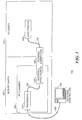
- Processor 120 is coupled to interface electronics 133 via a serial data control bus cable 125.
- a non-RF cavity 150 is used to house the processor 120 and the electronics outside the RF chamber 160.
- An external controller 170 such as a personal computer (PC), uses a number of external interfaces 165, either serial or parallel, e.g. RS232, to control the processor 120.
- Interface electronics 133 is operable to choose one or more of a plethora of input signals. The selected input signals are coupled to filtered connector 130. Filtered connector 130 is coupled to electronics 140 within RF cavity 110 by serial data control bus cable 135, which may be physically realized as one or more cables or printed circuit assemblies.
- Processor 120 is operable to transmit and receive one or more data signals using serial data control bus cable 125 to filtered connector 130.
- Filtered connector 130 isolates these one or more data signals and passes them to electronics 140 via serial data control bus cable 135.
- An addressing scheme is implemented by processor 120 so that only those serial bus lines that are used to control electronics 140 within RF cavity 110 are active.
- the selection of the one or more serial lines operable to enter RF cavity 110 is controlled by interface electronics 133.
- the use of a gating functionality to determine which signals are permitted to enter RF cavity 110 may additionally have a temporal aspect in that it may be used to selectively determine when such signals are permitted to enter RF cavity 110. This temporal aspect is an important advantage of the present invention. There may be times during the testing process when eliminating spurious noise is not important but other times, such as during noise sensitive measurements, which it can be critical.
- FIG. 2 an example of this addressing scheme is shown according to one embodiment of the present invention.
- This example uses eight addresses to control electronics internal and external to the RF cavity. Addresses 0,1,2, and 3 are operable to control one or more electronics elements within electronics 140. Addresses 4, 5, 6, and 7 are operable to control one or more elements within electronics outside the RF chamber 160.
- address line #1 is used to gate all signals that enter RF cavity 110. Thus only addresses 0, 1, 2, and 3 are active within the RF cavity.
- This gating functionality enabled through setting the value of line #1, allows a processor element to allow only those signals used to control electronics 140 enter the RF cavity. Those signals corresponding to addresses 4, 5, 6, and 7 are held in a quiescent mode within the RF cavity.
- the gating functionality may have a temporal characteristic in that interface electronics 133 can through the gating control when certain signals are allowed to enter RF cavity 110.
- interface electronics 133 is operable to be coupled directly to processor 120 without departing from the spirit and scope of the present invention. Further, electronics component 140 may be distributed in several locations within RF enclosure 110. Filtered connector 130 is operable to maintain connections with one or more of these distributed electronics components.
Landscapes
- Physics & Mathematics (AREA)
- Electromagnetism (AREA)
- General Physics & Mathematics (AREA)
- Engineering & Computer Science (AREA)
- Computer Networks & Wireless Communication (AREA)
- Signal Processing (AREA)
- Tests Of Electronic Circuits (AREA)
- Measurement Of The Respiration, Hearing Ability, Form, And Blood Characteristics Of Living Organisms (AREA)
Abstract
Description
Claims (6)
- A method of controlling a flow of serial data across an Radio Frequency (RF) barrier of an RF enclosure (110), comprising:a processor (120) sending one or more control data using one or more lines of a serial control data bus (125);an interface electronics module (133), receiving the one or more lines of the serial control data bus and selecting one or more signals corresponding to one or more addresses of the one or more lines; andthe interface electronics module, sending the selected one or more signals to an electronics module (140) within the RF enclosure.
- The method of claim 1, wherein sensing the selected one or more signals to the electronics module within the RF enclosure is performed in accordance with a gating functionality of the interface electronics module.
- The method of claim 2, wherein the gating functionality is a temporal gating functionality.
- A structure for controlling a flow of serial data across an Radio Frequency (RF) barrier of an RF enclosure, comprising:a processor (120), operable to send and receive data, coupled to one or more lines of a serial control data bus (125);
- The structure if claim 4, wherein an RF filtered connector (130) is coupled to the interface electronics module and to the RF enclosure, said RF enclosure providing an interface to the RF cavity.
- The structure of claim 5, wherein one or more Schmitt trigger input buffers are used to eliminate potential noise problems caused by the RF filtered connectors.
Applications Claiming Priority (2)
| Application Number | Priority Date | Filing Date | Title |
|---|---|---|---|
| US10/001,436 US6813646B2 (en) | 2001-10-31 | 2001-10-31 | Controlling electronics across an RF barrier using a serial interface bus |
| US1436 | 2001-10-31 |
Publications (3)
| Publication Number | Publication Date |
|---|---|
| EP1309238A2 true EP1309238A2 (en) | 2003-05-07 |
| EP1309238A3 EP1309238A3 (en) | 2004-12-22 |
| EP1309238B1 EP1309238B1 (en) | 2006-12-20 |
Family
ID=21696000
Family Applications (1)
| Application Number | Title | Priority Date | Filing Date |
|---|---|---|---|
| EP02257424A Expired - Lifetime EP1309238B1 (en) | 2001-10-31 | 2002-10-25 | Controlling data flow across an RF barrier |
Country Status (5)
| Country | Link |
|---|---|
| US (1) | US6813646B2 (en) |
| EP (1) | EP1309238B1 (en) |
| KR (1) | KR20030036048A (en) |
| DE (1) | DE60216878T2 (en) |
| TW (1) | TW576055B (en) |
Families Citing this family (2)
| Publication number | Priority date | Publication date | Assignee | Title |
|---|---|---|---|---|
| JP4484923B2 (en) * | 2007-12-27 | 2010-06-16 | 株式会社日立製作所 | Processor |
| US8281917B1 (en) * | 2012-05-23 | 2012-10-09 | Paradigm Circuit Solutions Inc. | System and method to automate transport of electronic devices on an assembly line for testing |
Family Cites Families (8)
| Publication number | Priority date | Publication date | Assignee | Title |
|---|---|---|---|---|
| FR2635191B1 (en) * | 1988-08-05 | 1990-10-05 | Merlin Gerin | METHOD AND DEVICE FOR CONTROLLING A QUASI-CLOSED ELECTROMAGNETIC SCREEN |
| US4962358A (en) * | 1989-04-27 | 1990-10-09 | The Curran Company | Integrity monitoring method and system for shielded enclosures having a fiber optic cable for bidirectional communications between a receiver and transmitter thereof |
| GB2248696B (en) * | 1990-10-12 | 1994-11-23 | Intepro Systems Dev Limited | A test apparatus and process |
| US5244415A (en) * | 1992-02-07 | 1993-09-14 | Harbor Electronics, Inc. | Shielded electrical connector and cable |
| US5383096A (en) * | 1993-05-03 | 1995-01-17 | Digital Equipment Corporation | I/O expansion box |
| US5561378A (en) * | 1994-07-05 | 1996-10-01 | Motorola, Inc. | Circuit probe for measuring a differential circuit |
| US5953206A (en) * | 1997-10-15 | 1999-09-14 | Hewlett-Packard Company | Thermal dissipation and EMI shielding structure for notebook computers |
| US6307538B1 (en) * | 1998-06-18 | 2001-10-23 | Microsoft Corporation | EMC enhanced peripheral device |
-
2001
- 2001-10-31 US US10/001,436 patent/US6813646B2/en not_active Expired - Fee Related
-
2002
- 2002-07-29 TW TW91116882A patent/TW576055B/en not_active IP Right Cessation
- 2002-10-25 DE DE60216878T patent/DE60216878T2/en not_active Expired - Fee Related
- 2002-10-25 EP EP02257424A patent/EP1309238B1/en not_active Expired - Lifetime
- 2002-10-30 KR KR1020020066516A patent/KR20030036048A/en not_active Ceased
Also Published As
| Publication number | Publication date |
|---|---|
| KR20030036048A (en) | 2003-05-09 |
| DE60216878T2 (en) | 2007-05-03 |
| US6813646B2 (en) | 2004-11-02 |
| EP1309238B1 (en) | 2006-12-20 |
| TW576055B (en) | 2004-02-11 |
| US20030082959A1 (en) | 2003-05-01 |
| DE60216878D1 (en) | 2007-02-01 |
| EP1309238A3 (en) | 2004-12-22 |
Similar Documents
| Publication | Publication Date | Title |
|---|---|---|
| EP2158495B1 (en) | Integrated circuit with self-test feature for validating functionality of external interfaces | |
| US7979745B2 (en) | On-chip debug emulator, debugging method, and microcomputer | |
| EP3660526B1 (en) | Test system with embedded tester | |
| US20060179374A1 (en) | Wireless hardware debugging | |
| US7752359B2 (en) | Wireless-interface module and electronic apparatus | |
| US6813646B2 (en) | Controlling electronics across an RF barrier using a serial interface bus | |
| US10156606B2 (en) | Multi-chassis test device and test signal transmission apparatus of the same | |
| TWI676040B (en) | Semiconductor integrated circuit test system and semiconductor integrated circuit test device thereof | |
| US20100156436A1 (en) | Integrated circuit and noise measuring method | |
| CN102062792B (en) | Probe card | |
| US4975602A (en) | Logic level data conversion system | |
| US20030237036A1 (en) | Semiconductor integrated circuit with built-in self-test function and system including the same | |
| CN213186126U (en) | An anti-jamming device and system for base station signals | |
| US5463311A (en) | Apparatus and method for measuring operating voltage electrical signals in a high voltage environment | |
| CN110824330A (en) | Semiconductor integrated circuit test system and semiconductor integrated circuit test device thereof | |
| CN116961784B (en) | A testing system and testing method for radio frequency chip receiving channel | |
| US7174132B2 (en) | RF transceiver arrangement, terminal employing the arrangement, and method for fabricating terminal according to the arrangement | |
| EP1695186A2 (en) | Configurable input/output terminals | |
| US12401382B2 (en) | Chip, system of noise analysis and method of noise analysis | |
| US7305603B1 (en) | Boundary scan cell and methods for integrating and operating the same | |
| KR100464451B1 (en) | Circuit for reducing leakage current of processor | |
| Michalak et al. | EMC in IoT world | |
| KR20050120350A (en) | Multiplexing apparatus of input/output port | |
| KR100617764B1 (en) | Mobile terminal and expansion connector for connecting to the verification device via the interface connector | |
| Srinivaas et al. | Development of portable radiation intensity meter |
Legal Events
| Date | Code | Title | Description |
|---|---|---|---|
| PUAI | Public reference made under article 153(3) epc to a published international application that has entered the european phase |
Free format text: ORIGINAL CODE: 0009012 |
|
| AK | Designated contracting states |
Designated state(s): AT BE BG CH CY CZ DE DK EE ES FI FR GB GR IE IT LI LU MC NL PT SE SK TR |
|
| AX | Request for extension of the european patent |
Extension state: AL LT LV MK RO SI |
|
| PUAL | Search report despatched |
Free format text: ORIGINAL CODE: 0009013 |
|
| AK | Designated contracting states |
Kind code of ref document: A3 Designated state(s): AT BE BG CH CY CZ DE DK EE ES FI FR GB GR IE IT LI LU MC NL PT SE SK TR |
|
| AX | Request for extension of the european patent |
Extension state: AL LT LV MK RO SI |
|
| 17P | Request for examination filed |
Effective date: 20050131 |
|
| AKX | Designation fees paid |
Designated state(s): DE FI FR |
|
| GRAP | Despatch of communication of intention to grant a patent |
Free format text: ORIGINAL CODE: EPIDOSNIGR1 |
|
| GRAS | Grant fee paid |
Free format text: ORIGINAL CODE: EPIDOSNIGR3 |
|
| GRAA | (expected) grant |
Free format text: ORIGINAL CODE: 0009210 |
|
| AK | Designated contracting states |
Kind code of ref document: B1 Designated state(s): DE FI FR |
|
| RAP2 | Party data changed (patent owner data changed or rights of a patent transferred) |
Owner name: AGILENT TECHNOLOGIES, INC. |
|
| REF | Corresponds to: |
Ref document number: 60216878 Country of ref document: DE Date of ref document: 20070201 Kind code of ref document: P |
|
| ET | Fr: translation filed | ||
| PLBE | No opposition filed within time limit |
Free format text: ORIGINAL CODE: 0009261 |
|
| STAA | Information on the status of an ep patent application or granted ep patent |
Free format text: STATUS: NO OPPOSITION FILED WITHIN TIME LIMIT |
|
| 26N | No opposition filed |
Effective date: 20070921 |
|
| PGFP | Annual fee paid to national office [announced via postgrant information from national office to epo] |
Ref country code: DE Payment date: 20071130 Year of fee payment: 6 |
|
| PGFP | Annual fee paid to national office [announced via postgrant information from national office to epo] |
Ref country code: FI Payment date: 20071030 Year of fee payment: 6 |
|
| PGFP | Annual fee paid to national office [announced via postgrant information from national office to epo] |
Ref country code: FR Payment date: 20071017 Year of fee payment: 6 |
|
| REG | Reference to a national code |
Ref country code: FR Ref legal event code: ST Effective date: 20090630 |
|
| PG25 | Lapsed in a contracting state [announced via postgrant information from national office to epo] |
Ref country code: FI Free format text: LAPSE BECAUSE OF NON-PAYMENT OF DUE FEES Effective date: 20081025 |
|
| PG25 | Lapsed in a contracting state [announced via postgrant information from national office to epo] |
Ref country code: DE Free format text: LAPSE BECAUSE OF NON-PAYMENT OF DUE FEES Effective date: 20090501 |
|
| PG25 | Lapsed in a contracting state [announced via postgrant information from national office to epo] |
Ref country code: FR Free format text: LAPSE BECAUSE OF NON-PAYMENT OF DUE FEES Effective date: 20081031 |