EP1309042B1 - Federblech zum Kontaktieren eines Bauteils auf einer Leiterplatte - Google Patents
Federblech zum Kontaktieren eines Bauteils auf einer Leiterplatte Download PDFInfo
- Publication number
- EP1309042B1 EP1309042B1 EP02022921A EP02022921A EP1309042B1 EP 1309042 B1 EP1309042 B1 EP 1309042B1 EP 02022921 A EP02022921 A EP 02022921A EP 02022921 A EP02022921 A EP 02022921A EP 1309042 B1 EP1309042 B1 EP 1309042B1
- Authority
- EP
- European Patent Office
- Prior art keywords
- circuit board
- component
- spring
- spring plate
- circuit
- Prior art date
- Legal status (The legal status is an assumption and is not a legal conclusion. Google has not performed a legal analysis and makes no representation as to the accuracy of the status listed.)
- Expired - Lifetime
Links
Images

Classifications
-
- H—ELECTRICITY
- H01—ELECTRIC ELEMENTS
- H01R—ELECTRICALLY-CONDUCTIVE CONNECTIONS; STRUCTURAL ASSOCIATIONS OF A PLURALITY OF MUTUALLY-INSULATED ELECTRICAL CONNECTING ELEMENTS; COUPLING DEVICES; CURRENT COLLECTORS
- H01R24/00—Two-part coupling devices, or either of their cooperating parts, characterised by their overall structure
- H01R24/38—Two-part coupling devices, or either of their cooperating parts, characterised by their overall structure having concentrically or coaxially arranged contacts
- H01R24/40—Two-part coupling devices, or either of their cooperating parts, characterised by their overall structure having concentrically or coaxially arranged contacts specially adapted for high frequency
- H01R24/50—Two-part coupling devices, or either of their cooperating parts, characterised by their overall structure having concentrically or coaxially arranged contacts specially adapted for high frequency mounted on a PCB [Printed Circuit Board]
-
- H—ELECTRICITY
- H05—ELECTRIC TECHNIQUES NOT OTHERWISE PROVIDED FOR
- H05K—PRINTED CIRCUITS; CASINGS OR CONSTRUCTIONAL DETAILS OF ELECTRIC APPARATUS; MANUFACTURE OF ASSEMBLAGES OF ELECTRICAL COMPONENTS
- H05K1/00—Printed circuits
- H05K1/02—Details
- H05K1/0213—Electrical arrangements not otherwise provided for
- H05K1/0237—High frequency adaptations
- H05K1/0243—Printed circuits associated with mounted high frequency components
-
- H—ELECTRICITY
- H05—ELECTRIC TECHNIQUES NOT OTHERWISE PROVIDED FOR
- H05K—PRINTED CIRCUITS; CASINGS OR CONSTRUCTIONAL DETAILS OF ELECTRIC APPARATUS; MANUFACTURE OF ASSEMBLAGES OF ELECTRICAL COMPONENTS
- H05K3/00—Apparatus or processes for manufacturing printed circuits
- H05K3/30—Assembling printed circuits with electric components, e.g. with resistors
- H05K3/32—Assembling printed circuits with electric components, e.g. with resistors electrically connecting electric components or wires to printed circuits
- H05K3/325—Assembling printed circuits with electric components, e.g. with resistors electrically connecting electric components or wires to printed circuits by abutting or pinching; Mechanical auxiliary parts therefor
-
- H—ELECTRICITY
- H01—ELECTRIC ELEMENTS
- H01R—ELECTRICALLY-CONDUCTIVE CONNECTIONS; STRUCTURAL ASSOCIATIONS OF A PLURALITY OF MUTUALLY-INSULATED ELECTRICAL CONNECTING ELEMENTS; COUPLING DEVICES; CURRENT COLLECTORS
- H01R12/00—Structural associations of a plurality of mutually-insulated electrical connecting elements, specially adapted for printed circuits, e.g. printed circuit boards [PCB], flat or ribbon cables, or like generally planar structures, e.g. terminal strips, terminal blocks; Coupling devices specially adapted for printed circuits, flat or ribbon cables, or like generally planar structures; Terminals specially adapted for contact with, or insertion into, printed circuits, flat or ribbon cables, or like generally planar structures
- H01R12/50—Fixed connections
- H01R12/51—Fixed connections for rigid printed circuits or like structures
- H01R12/55—Fixed connections for rigid printed circuits or like structures characterised by the terminals
- H01R12/58—Fixed connections for rigid printed circuits or like structures characterised by the terminals terminals for insertion into holes
- H01R12/585—Terminals having a press fit or a compliant portion and a shank passing through a hole in the printed circuit board
-
- H—ELECTRICITY
- H01—ELECTRIC ELEMENTS
- H01R—ELECTRICALLY-CONDUCTIVE CONNECTIONS; STRUCTURAL ASSOCIATIONS OF A PLURALITY OF MUTUALLY-INSULATED ELECTRICAL CONNECTING ELEMENTS; COUPLING DEVICES; CURRENT COLLECTORS
- H01R13/00—Details of coupling devices of the kinds covered by groups H01R12/70 or H01R24/00 - H01R33/00
- H01R13/02—Contact members
- H01R13/22—Contacts for co-operating by abutting
- H01R13/24—Contacts for co-operating by abutting resilient; resiliently-mounted
-
- H—ELECTRICITY
- H01—ELECTRIC ELEMENTS
- H01R—ELECTRICALLY-CONDUCTIVE CONNECTIONS; STRUCTURAL ASSOCIATIONS OF A PLURALITY OF MUTUALLY-INSULATED ELECTRICAL CONNECTING ELEMENTS; COUPLING DEVICES; CURRENT COLLECTORS
- H01R2103/00—Two poles
-
- H—ELECTRICITY
- H01—ELECTRIC ELEMENTS
- H01R—ELECTRICALLY-CONDUCTIVE CONNECTIONS; STRUCTURAL ASSOCIATIONS OF A PLURALITY OF MUTUALLY-INSULATED ELECTRICAL CONNECTING ELEMENTS; COUPLING DEVICES; CURRENT COLLECTORS
- H01R31/00—Coupling parts supported only by co-operation with counterpart
- H01R31/08—Short-circuiting members for bridging contacts in a counterpart
-
- H—ELECTRICITY
- H05—ELECTRIC TECHNIQUES NOT OTHERWISE PROVIDED FOR
- H05K—PRINTED CIRCUITS; CASINGS OR CONSTRUCTIONAL DETAILS OF ELECTRIC APPARATUS; MANUFACTURE OF ASSEMBLAGES OF ELECTRICAL COMPONENTS
- H05K2201/00—Indexing scheme relating to printed circuits covered by H05K1/00
- H05K2201/09—Shape and layout
- H05K2201/09209—Shape and layout details of conductors
- H05K2201/09654—Shape and layout details of conductors covering at least two types of conductors provided for in H05K2201/09218 - H05K2201/095
- H05K2201/09809—Coaxial layout
-
- H—ELECTRICITY
- H05—ELECTRIC TECHNIQUES NOT OTHERWISE PROVIDED FOR
- H05K—PRINTED CIRCUITS; CASINGS OR CONSTRUCTIONAL DETAILS OF ELECTRIC APPARATUS; MANUFACTURE OF ASSEMBLAGES OF ELECTRICAL COMPONENTS
- H05K2201/00—Indexing scheme relating to printed circuits covered by H05K1/00
- H05K2201/10—Details of components or other objects attached to or integrated in a printed circuit board
- H05K2201/10007—Types of components
- H05K2201/10189—Non-printed connector
-
- H—ELECTRICITY
- H05—ELECTRIC TECHNIQUES NOT OTHERWISE PROVIDED FOR
- H05K—PRINTED CIRCUITS; CASINGS OR CONSTRUCTIONAL DETAILS OF ELECTRIC APPARATUS; MANUFACTURE OF ASSEMBLAGES OF ELECTRICAL COMPONENTS
- H05K2201/00—Indexing scheme relating to printed circuits covered by H05K1/00
- H05K2201/10—Details of components or other objects attached to or integrated in a printed circuit board
- H05K2201/10431—Details of mounted components
- H05K2201/1059—Connections made by press-fit insertion
-
- H—ELECTRICITY
- H05—ELECTRIC TECHNIQUES NOT OTHERWISE PROVIDED FOR
- H05K—PRINTED CIRCUITS; CASINGS OR CONSTRUCTIONAL DETAILS OF ELECTRIC APPARATUS; MANUFACTURE OF ASSEMBLAGES OF ELECTRICAL COMPONENTS
- H05K2201/00—Indexing scheme relating to printed circuits covered by H05K1/00
- H05K2201/10—Details of components or other objects attached to or integrated in a printed circuit board
- H05K2201/10613—Details of electrical connections of non-printed components, e.g. special leads
- H05K2201/10742—Details of leads
- H05K2201/1075—Shape details
- H05K2201/10856—Divided leads, e.g. by slot in length direction of lead, or by branching of the lead
-
- H—ELECTRICITY
- H05—ELECTRIC TECHNIQUES NOT OTHERWISE PROVIDED FOR
- H05K—PRINTED CIRCUITS; CASINGS OR CONSTRUCTIONAL DETAILS OF ELECTRIC APPARATUS; MANUFACTURE OF ASSEMBLAGES OF ELECTRICAL COMPONENTS
- H05K3/00—Apparatus or processes for manufacturing printed circuits
- H05K3/30—Assembling printed circuits with electric components, e.g. with resistors
- H05K3/306—Assembling printed circuits with electric components, e.g. with resistors with lead-in-hole components
- H05K3/308—Adaptations of leads
Definitions
- the present invention relates to a spring plate for an electrical or electronic component with spring pins for mounting on a printed circuit board according to The preamble of claim 1.
- the invention further relates to a Circuit arrangement with a printed circuit board and at least one electrical or electronic component with spring pins for fixing the component on the Printed circuit board according to the preamble of claim 2.
- the long spring pins shine RF energy, on the other hand, it may be to injections of RF energy in the High frequency circuit via the acting as an antenna spring pins come.
- This Problem is exacerbated by the fact that between component and contact to PCB over the spring pins no exact impedance control prevails. Since that Component does not rest directly on the circuit board, but a certain Distance that has a gap between the component and circuit board, there is in Area of the spring pins an unshielded area, the radiation and Coupling also favored in an undesirable manner.
- the invention is based on the object, a spring plate and a Circuitry of o.g. To improve the type of RF properties, without losing the advantage of simple process design during production. Furthermore, a backward compatibility to previous processes assemblies remain.
- the Spring plate is formed as a square with a central circular recess, wherein the circular recess on the diagonal of the square additional Bulges, wherein the spring plate at least one resilient, has arcuate elevation, so that when the spring plate between the component and Circuit board is arranged at least one electrical contact between at least a part of the component and at least one corresponding contact surface on the PCB instead of at least one spring pin manufactures.
- the spring pins on the function "bracket” and on the other hand, the spring plate on the function "electrical contact” independently be optimized from each other. Furthermore, there is no need for HF applications unwanted input or radiation of RF energy via such spring pins, the no longer make electrical contact and a corresponding RF signal have to transfer. In addition, there is an impedance-controlled transition from the component to the circuit board without soldering technique and without pure surface-mount technology and possibly ensured without modification of components, circuit board and manufacturing process. This can be used for existing applications or processes Backward compatibility with better RF characteristics at the same time become.
- a spring plate is, which is formed as a square with a central circular recess is, with the circular recess on the diagonal of the square Having additional bulges and wherein the spring plate at least one having resilient, arcuate elevation, so that the spring plate at least an electrical contact between at least a part of the component and at least one corresponding contact surface on the circuit board instead at least one spring pin manufactures.
- the component has a housing made of a conductive material and the spring plate is formed such that there is an electrical contact between the housing and produces corresponding ground contacts on the circuit board.
- the component is an RF component, in particular a coaxial coupler.
- An optimal adaptation to the component such that spring pins of the component through The spring plate can reach through the fact that the spring plate a circumferential geometry, which corresponds to a circumferential geometry of the component, and in the region of the spring pins of the component has at least one recess.
- contact surface on the circuit board comprises at least one Conductor coating a via of the circuit board and / or at least a footprint on the circuit board.
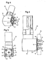
- an inventive Spring plate 10 is a square with a central, circular opening 12 formed. On the diagonal of the square is the central, circular Opening 12 provided with additional recesses 14. The areas 16 form resilient elevations.
- the spring plate 10 is formed such that it in its square peripheral geometry of a peripheral geometry of a housing 18 corresponds to a Koaxialwinkelsteckers 20 at the contacting side, wherein the additional recesses 14 formed exactly in the places are at which outer spring pins 22 from the Koaxialwinkelstecker 20th rise.
- the central, circular opening 12 of the spring plate 10 allows a central spring pin 24 of the Koaxialwinkelsteckers 20 the passage of the Spring plate 10.
- To shield the housing 18 is made of metal.
- This Koaxialwinkelstecker 20 serves as a coaxial coupler to a circuit on a PCB.
- the outer spring pins 22 are intended to make an electrical contact a ground potential on the circuit board and the middle spring pin 24 is a making electrical contact with a signal line on the circuit board.
- Fig. 6 schematically illustrates a Koaxialwinkelstecker 20, which on a printed circuit board 26 is mounted, wherein the spring plate 10 between Koaxialwinkelsteckers 20 and circuit board 26 is arranged.
- the spring plate 10 contacted by the resilient action of the sections 16 on the one hand, the metallic housing 18 and on the other hand in the field of resilient surveys 16 corresponding Metal coatings (not shown) of plated-through holes (not shown) on the printed circuit board 26.
- the ground contact does not over the spring pins 22, but directly in the manner of a "surface mount" between housing 18 PCB and metallized PCB surface.
- the spring pins 22 are thus electrically bridged and at the same time the gap between the circuit board 26 and housing 18 of a shield in the form of the circumferential spring plate surrounded and thus shielded. This also makes the contact between the Koaxialwinkelstecker 20 and the circuit board 26 impedance controlled.
- the remarkable thing here is that neither the Koaxialwinkelstecker 20 nor the Surface design of the circuit board 26 must be adapted.
- the spring plate 10 takes advantage of the existing conditions, namely that the housing 18 of the Koaxialwinkelsteckers 20 is made of metal and that the conductor coating from vias to the surface of the circuit board is sufficient.
- already existing processes and Components have a considerably improved contacting with regard to the HF characteristic between Koaxialwinkelstecker 20 and PCB 26 achieved.
- the radiation and Coupling of RF energy in the region of the gap between Koaxialwinkelstekker 20 and circuit board 26 or via the spring pins 22, 24 is substantially reduced, whereby the entire circuit arrangement without modifications, for example on the layout of the circuit on the circuit board 26, even at higher frequencies can be operated.
- a local proximity of an RF path and a digital Path on the circuit board 26 is not critical.
- the circuit board 26 instead of the metallization of the holes for the spring pins 22 a so-called. Footprint provided, the corresponding contact surfaces for the spring plate 10 on the circuit board 26 is available.
- the function of holding the component is always advantageous 20 of the function of the electrical contacting of the component 20 with a Circuit on the circuit board 26 separated.
- the spring pins 22 are used exclusively the holder, while the spring plate 10 only the contact serves.
Landscapes
- Engineering & Computer Science (AREA)
- Microelectronics & Electronic Packaging (AREA)
- Metallurgy (AREA)
- Manufacturing & Machinery (AREA)
- Coupling Device And Connection With Printed Circuit (AREA)
- Multi-Conductor Connections (AREA)
- Contacts (AREA)
- Push-Button Switches (AREA)
- Manufacturing Of Printed Wiring (AREA)
- Shielding Devices Or Components To Electric Or Magnetic Fields (AREA)
Description
- Fig. 1
- eine bevorzugte Ausführungsform eines erfindungsgemäßen Federbleches in Aufsicht,
- Fig. 2
- in Seitenansicht,
- Fig. 3
- in perspektivischer Ansicht,
- Fig. 4
- ein Bauteil in Form eines Koaxialwinkelsteckers mit dem Federblech gemäß Fig. 1 in perspektivischer Ansicht,
- Fig. 5
- in einer Ansicht von unten und
- Fig. 6
- das Bauteil gemäß Fig. 4 nach Montage auf einer Leiterplatte in schematischer Seitenansicht.
Claims (7)
- Federblech (10) für ein elektrisches bzw. elektronisches Bauteil (20) mit Federstiften (22, 24) zum Befestigen auf einer Leiterplatte (26),
dadurch gekennzeichnet, dass das Federblech (10) als Quadrat mit einer mittigen kreisförmigen Ausnehmung (12) ausgebildet ist, wobei die kreisförmige Ausnehmung (12) auf den Diagonalen des Quadrats zusätzliche Ausbuchtungen (14) aufweist, wobei das Federblech (10) wenigstens eine federnde, bogenförmige Erhebung (16) aufweist, so dass wenn das Federblech (10) zwischen Bauteil (20) und Leiterplatte (26) angeordnet ist wenigstens ein elektrischer Kontakt zwischen wenigstens einem Teil (18) des Bauteils (20) und wenigstens einer entsprechenden Kontaktfläche auf der Leiterplatte (26) hergestellt ist. - Schaltungsanordnung mit einer Leiterplatte (26) und wenigstens einem elektrischen bzw. elektronischen Bauteil (20) mit Federstiften (22, 24) zum Befestigen des Bauteils (20) auf der Leiterplatte (26),
dadurch gekennzeichnet, dass zwischen Leiterplatte (26) und wenigstens einem Bauteil (20) ein Federblech (10) angeordnet ist, welches als Quadrat mit einer mittigen kreisförmigen Ausnehmung (12) ausgebildet ist, wobei die kreisförmige Ausnehmung (12) auf den Diagonalen des Quadrats zusätzliche Ausbuchtungen (14) aufweist und wobei das Federblech (10) wenigstens eine federnde, bogenförmige Erhebung (16) aufweist, so dass das Federblech (10) wenigstens einen elektrischen Kontakt zwischen wenigstens einem Teil des Bauteils (20) und wenigstens einer entsprechenden Kontaktfläche auf der Leiterplatte (26) anstatt wenigstens eines Federstiftes (22) herstellt. - Schaltungsanordnung nach Anspruch 2, dadurch gekennzeichnet, dass das Bauteil (20) ein Gehäuse (18) aus einem leitenden Werkstoff aufweist und das Federblech (10) derart ausgebildet ist, daß es einen elektrischen Kontakt zwischen dem Gehäuse (18) und entsprechenden Massekontakten auf der Leiterplatte (26) herstellt.
- Schaltungsanordnung nach Anspruch 2 oder 3, dadurch gekennzeichnet, dass das Bauteil (20) ein HF-Bauteil, insbesondere ein Koaxialkuppler, ist.
- Schaltungsanordnung nach einem der Ansprüche 2 bis 4, dadurch gekennzeichnet, daß dieses eine Umfangsgeometrie aufweist, welche einer Umfangsgeometrie des Bauteils (20) entspricht, und im Bereich der Federstifte (22, 24) des Bauteils (20) wenigstens eine Ausnehmung (12, 14) aufweist.
- Schaltungsanordnung nach einem der Ansprüche 2 bis 5, dadurch gekennzeichnet, dass die Kontaktfläche auf der Leiterplatte (26) wenigstens eine Leiterbeschichtung einer Durchkontaktierung der Leiterplatte (26) umfaßt.
- Schaltungsanordnung nach einem der Ansprüche 2 bis 6, dadurch gekennzeichnet, dass die Kontaktfläche auf der Leiterplatte (26) wenigstens einen Footprint auf der Leiterplatte (26) umfaßt.
Applications Claiming Priority (2)
| Application Number | Priority Date | Filing Date | Title |
|---|---|---|---|
| DE20117997U DE20117997U1 (de) | 2001-11-05 | 2001-11-05 | Federblech zum Kontaktieren eines Bauteils auf einer Leiterplatte sowie Schaltungsanordnung mit kontaktierendem Federblech |
| DE20117997U | 2001-11-05 |
Publications (3)
| Publication Number | Publication Date |
|---|---|
| EP1309042A2 EP1309042A2 (de) | 2003-05-07 |
| EP1309042A3 EP1309042A3 (de) | 2004-04-21 |
| EP1309042B1 true EP1309042B1 (de) | 2005-12-28 |
Family
ID=7963602
Family Applications (1)
| Application Number | Title | Priority Date | Filing Date |
|---|---|---|---|
| EP02022921A Expired - Lifetime EP1309042B1 (de) | 2001-11-05 | 2002-10-10 | Federblech zum Kontaktieren eines Bauteils auf einer Leiterplatte |
Country Status (3)
| Country | Link |
|---|---|
| EP (1) | EP1309042B1 (de) |
| AT (1) | ATE314745T1 (de) |
| DE (2) | DE20117997U1 (de) |
Families Citing this family (4)
| Publication number | Priority date | Publication date | Assignee | Title |
|---|---|---|---|---|
| DE202012007216U1 (de) * | 2012-07-25 | 2012-08-20 | Rosenberger Hochfrequenztechnik Gmbh & Co. Kg | Kontaktelement |
| DE102014018036A1 (de) | 2014-12-05 | 2015-06-18 | Daimler Ag | Elektrische Verbindung |
| DE102021201661A1 (de) * | 2021-02-22 | 2022-08-25 | Vega Grieshaber Kg | Kontaktierungseinheit für einen Impedanzgrenzschalter |
| DE102024127927A1 (de) * | 2024-09-26 | 2026-03-26 | Md Elektronik Gmbh | Platinensteckverbinder und platine |
Family Cites Families (9)
| Publication number | Priority date | Publication date | Assignee | Title |
|---|---|---|---|---|
| US4626812A (en) * | 1983-08-12 | 1986-12-02 | Omron Tateisi Electronics Co. | Electromagnetic relay for switching high frequency signals |
| DE3430589A1 (de) * | 1984-08-20 | 1986-02-27 | Siemens AG, 1000 Berlin und 8000 München | Sockel fuer ein elektromagnetisches relais |
| US4737123A (en) | 1987-04-15 | 1988-04-12 | Watkins-Johnson Company | Connector assembly for packaged microwave integrated circuits |
| FR2618250B1 (fr) * | 1987-07-16 | 1989-11-17 | Merlin Gerin | Commutateur de reglage pour une carte a circuit imprime. |
| US5092783A (en) | 1991-05-16 | 1992-03-03 | Motorola, Inc. | RF interconnect |
| US5178562A (en) * | 1991-10-17 | 1993-01-12 | Epson Portland, Inc. | Contact member for miniature electrical circuit connector |
| NL9300971A (nl) | 1993-06-04 | 1995-01-02 | Framatome Connectors Belgium | Connectorsamenstel voor printkaarten. |
| DE19600966C2 (de) | 1996-01-12 | 2000-09-07 | Siemens Ag | Kontaktfeder zum elektrischen Kontaktieren eines Bauteils |
| DE19720678C1 (de) | 1997-05-16 | 1998-10-08 | Siemens Ag | HF-Koaxial-Steckverbinderteil |
-
2001
- 2001-11-05 DE DE20117997U patent/DE20117997U1/de not_active Expired - Lifetime
-
2002
- 2002-10-10 EP EP02022921A patent/EP1309042B1/de not_active Expired - Lifetime
- 2002-10-10 DE DE50205421T patent/DE50205421D1/de not_active Expired - Lifetime
- 2002-10-10 AT AT02022921T patent/ATE314745T1/de active
Also Published As
| Publication number | Publication date |
|---|---|
| DE50205421D1 (de) | 2006-02-02 |
| EP1309042A2 (de) | 2003-05-07 |
| ATE314745T1 (de) | 2006-01-15 |
| DE20117997U1 (de) | 2002-02-14 |
| EP1309042A3 (de) | 2004-04-21 |
Similar Documents
| Publication | Publication Date | Title |
|---|---|---|
| DE69027012T2 (de) | Verbesserter Leiterplattenrandverbinder | |
| DE69519226T2 (de) | Verbinder mit integrierter Flachbaugruppe | |
| DE69322810T2 (de) | Hochfrequenz-Rückwandverbinder mit geschützter Kammer | |
| DE69200695T2 (de) | Filterverbinder. | |
| DE102009016757B4 (de) | Abschirmverbindung | |
| EP0247662A1 (de) | Durchführungsanschluss für HF-Signale | |
| DE10006530A1 (de) | Antennenfeder | |
| DE10142655A1 (de) | Bauelementanordnung | |
| EP3593412B1 (de) | Innenleiter-element und verfahren zum herstellen eines systems | |
| DE19510236A1 (de) | Flächige Antenne mit niedriger Bauhöhe | |
| DE69803920T2 (de) | Koaxialverbinder für gedruckte schaltungen | |
| EP0941644B1 (de) | Elektronischer schaltkreis mit einem hockfrequenzbedämpfenden schirmgehäuse | |
| EP3605746B1 (de) | Steckverbinder sowie steckverbindung mit einem solchen steckverbinder | |
| EP1714533B1 (de) | Elektrische baugruppe mit einem elektrisch leitfähigen kontaktstift zum einpressen in eine öffnung einer leiterplatte | |
| DE69420144T2 (de) | Elektrisches Stiftfeld auf einer Leiterplatte | |
| DE69714444T2 (de) | Keramikfilter mit koplanarer abschirmung | |
| DE102018118224B4 (de) | Kantenrand-Steckverbinder sowie Leiterplattenanordnung | |
| EP0828412B1 (de) | HF-Modul, z.B. Tuner | |
| EP2037541A2 (de) | Steckverbinder mit Platine | |
| DE102012005812A1 (de) | Elektrischer Verbinder mit integriertem Impedanzangleichelement | |
| DE60100358T2 (de) | Koaxial-steckverbinder und anordnung mit einem solchen verbinder | |
| EP1309042A2 (de) | Federblech zum Kontaktieren eines Bauteils auf einer Leiterplatte | |
| DE19851868C1 (de) | Elektrisches Leiterplatten-Bauteil und Verfahren zur automatischen Bestückung von Leiterplatten mit solchen Bauteilen | |
| WO2020021091A1 (de) | Kantenrand-steckverbinder sowie leiterplattenanordnung | |
| EP0878870A1 (de) | HF-Koaxial-Steckverbinderteil |
Legal Events
| Date | Code | Title | Description |
|---|---|---|---|
| PUAI | Public reference made under article 153(3) epc to a published international application that has entered the european phase |
Free format text: ORIGINAL CODE: 0009012 |
|
| AK | Designated contracting states |
Designated state(s): AT BE BG CH CY CZ DE DK EE ES FI FR GB GR IE IT LI LU MC NL PT SE SK TR |
|
| AX | Request for extension of the european patent |
Extension state: AL LT LV MK RO SI |
|
| PUAL | Search report despatched |
Free format text: ORIGINAL CODE: 0009013 |
|
| AK | Designated contracting states |
Kind code of ref document: A3 Designated state(s): AT BE BG CH CY CZ DE DK EE ES FI FR GB GR IE IT LI LU MC NL PT SE SK TR |
|
| AX | Request for extension of the european patent |
Extension state: AL LT LV MK RO SI |
|
| 17P | Request for examination filed |
Effective date: 20040922 |
|
| 17Q | First examination report despatched |
Effective date: 20041015 |
|
| AKX | Designation fees paid |
Designated state(s): AT BE BG CH CY CZ DE DK EE ES FI FR GB GR IE IT LI LU MC NL PT SE SK TR |
|
| GRAP | Despatch of communication of intention to grant a patent |
Free format text: ORIGINAL CODE: EPIDOSNIGR1 |
|
| RTI1 | Title (correction) |
Free format text: CONTACT SPRING FOR A COMPONENT ON A PRINT BOARD |
|
| GRAS | Grant fee paid |
Free format text: ORIGINAL CODE: EPIDOSNIGR3 |
|
| GRAA | (expected) grant |
Free format text: ORIGINAL CODE: 0009210 |
|
| AK | Designated contracting states |
Kind code of ref document: B1 Designated state(s): AT BE BG CH CY CZ DE DK EE ES FI FR GB GR IE IT LI LU MC NL PT SE SK TR |
|
| PG25 | Lapsed in a contracting state [announced via postgrant information from national office to epo] |
Ref country code: IE Free format text: LAPSE BECAUSE OF FAILURE TO SUBMIT A TRANSLATION OF THE DESCRIPTION OR TO PAY THE FEE WITHIN THE PRESCRIBED TIME-LIMIT Effective date: 20051228 Ref country code: IT Free format text: LAPSE BECAUSE OF FAILURE TO SUBMIT A TRANSLATION OF THE DESCRIPTION OR TO PAY THE FEE WITHIN THE PRESCRIBED TIME-LIMIT;WARNING: LAPSES OF ITALIAN PATENTS WITH EFFECTIVE DATE BEFORE 2007 MAY HAVE OCCURRED AT ANY TIME BEFORE 2007. THE CORRECT EFFECTIVE DATE MAY BE DIFFERENT FROM THE ONE RECORDED. Effective date: 20051228 Ref country code: CZ Free format text: LAPSE BECAUSE OF FAILURE TO SUBMIT A TRANSLATION OF THE DESCRIPTION OR TO PAY THE FEE WITHIN THE PRESCRIBED TIME-LIMIT Effective date: 20051228 Ref country code: SK Free format text: LAPSE BECAUSE OF FAILURE TO SUBMIT A TRANSLATION OF THE DESCRIPTION OR TO PAY THE FEE WITHIN THE PRESCRIBED TIME-LIMIT Effective date: 20051228 Ref country code: NL Free format text: LAPSE BECAUSE OF FAILURE TO SUBMIT A TRANSLATION OF THE DESCRIPTION OR TO PAY THE FEE WITHIN THE PRESCRIBED TIME-LIMIT Effective date: 20051228 Ref country code: FI Free format text: LAPSE BECAUSE OF FAILURE TO SUBMIT A TRANSLATION OF THE DESCRIPTION OR TO PAY THE FEE WITHIN THE PRESCRIBED TIME-LIMIT Effective date: 20051228 |
|
| REG | Reference to a national code |
Ref country code: GB Ref legal event code: FG4D Free format text: NOT ENGLISH |
|
| REG | Reference to a national code |
Ref country code: CH Ref legal event code: EP |
|
| REG | Reference to a national code |
Ref country code: IE Ref legal event code: FG4D Free format text: LANGUAGE OF EP DOCUMENT: GERMAN |
|
| REF | Corresponds to: |
Ref document number: 50205421 Country of ref document: DE Date of ref document: 20060202 Kind code of ref document: P |
|
| REG | Reference to a national code |
Ref country code: CH Ref legal event code: NV Representative=s name: HANS RUDOLF GACHNANG PATENTANWALT |
|
| GBT | Gb: translation of ep patent filed (gb section 77(6)(a)/1977) |
Effective date: 20060222 |
|
| PG25 | Lapsed in a contracting state [announced via postgrant information from national office to epo] |
Ref country code: GR Free format text: LAPSE BECAUSE OF FAILURE TO SUBMIT A TRANSLATION OF THE DESCRIPTION OR TO PAY THE FEE WITHIN THE PRESCRIBED TIME-LIMIT Effective date: 20060328 Ref country code: BG Free format text: LAPSE BECAUSE OF FAILURE TO SUBMIT A TRANSLATION OF THE DESCRIPTION OR TO PAY THE FEE WITHIN THE PRESCRIBED TIME-LIMIT Effective date: 20060328 Ref country code: SE Free format text: LAPSE BECAUSE OF FAILURE TO SUBMIT A TRANSLATION OF THE DESCRIPTION OR TO PAY THE FEE WITHIN THE PRESCRIBED TIME-LIMIT Effective date: 20060328 Ref country code: DK Free format text: LAPSE BECAUSE OF FAILURE TO SUBMIT A TRANSLATION OF THE DESCRIPTION OR TO PAY THE FEE WITHIN THE PRESCRIBED TIME-LIMIT Effective date: 20060328 |
|
| PG25 | Lapsed in a contracting state [announced via postgrant information from national office to epo] |
Ref country code: ES Free format text: LAPSE BECAUSE OF FAILURE TO SUBMIT A TRANSLATION OF THE DESCRIPTION OR TO PAY THE FEE WITHIN THE PRESCRIBED TIME-LIMIT Effective date: 20060408 |
|
| PG25 | Lapsed in a contracting state [announced via postgrant information from national office to epo] |
Ref country code: PT Free format text: LAPSE BECAUSE OF FAILURE TO SUBMIT A TRANSLATION OF THE DESCRIPTION OR TO PAY THE FEE WITHIN THE PRESCRIBED TIME-LIMIT Effective date: 20060529 |
|
| NLV1 | Nl: lapsed or annulled due to failure to fulfill the requirements of art. 29p and 29m of the patents act | ||
| REG | Reference to a national code |
Ref country code: IE Ref legal event code: FD4D |
|
| ET | Fr: translation filed | ||
| PG25 | Lapsed in a contracting state [announced via postgrant information from national office to epo] |
Ref country code: MC Free format text: LAPSE BECAUSE OF NON-PAYMENT OF DUE FEES Effective date: 20061031 |
|
| PLBE | No opposition filed within time limit |
Free format text: ORIGINAL CODE: 0009261 |
|
| STAA | Information on the status of an ep patent application or granted ep patent |
Free format text: STATUS: NO OPPOSITION FILED WITHIN TIME LIMIT |
|
| 26N | No opposition filed |
Effective date: 20060929 |
|
| BERE | Be: lapsed |
Owner name: ROSENBERGER HOCHFREQUENZTECHNIK G.M.B.H. & CO. Effective date: 20061031 |
|
| PG25 | Lapsed in a contracting state [announced via postgrant information from national office to epo] |
Ref country code: EE Free format text: LAPSE BECAUSE OF FAILURE TO SUBMIT A TRANSLATION OF THE DESCRIPTION OR TO PAY THE FEE WITHIN THE PRESCRIBED TIME-LIMIT Effective date: 20051228 |
|
| PG25 | Lapsed in a contracting state [announced via postgrant information from national office to epo] |
Ref country code: TR Free format text: LAPSE BECAUSE OF FAILURE TO SUBMIT A TRANSLATION OF THE DESCRIPTION OR TO PAY THE FEE WITHIN THE PRESCRIBED TIME-LIMIT Effective date: 20051228 |
|
| PG25 | Lapsed in a contracting state [announced via postgrant information from national office to epo] |
Ref country code: CY Free format text: LAPSE BECAUSE OF FAILURE TO SUBMIT A TRANSLATION OF THE DESCRIPTION OR TO PAY THE FEE WITHIN THE PRESCRIBED TIME-LIMIT Effective date: 20051228 |
|
| PG25 | Lapsed in a contracting state [announced via postgrant information from national office to epo] |
Ref country code: BE Free format text: LAPSE BECAUSE OF FAILURE TO SUBMIT A TRANSLATION OF THE DESCRIPTION OR TO PAY THE FEE WITHIN THE PRESCRIBED TIME-LIMIT Effective date: 20061031 |
|
| REG | Reference to a national code |
Ref country code: CH Ref legal event code: NV Representative=s name: GACHNANG AG PATENTANWAELTE, CH |
|
| REG | Reference to a national code |
Ref country code: FR Ref legal event code: PLFP Year of fee payment: 14 |
|
| REG | Reference to a national code |
Ref country code: FR Ref legal event code: PLFP Year of fee payment: 15 |
|
| REG | Reference to a national code |
Ref country code: FR Ref legal event code: PLFP Year of fee payment: 16 |
|
| REG | Reference to a national code |
Ref country code: FR Ref legal event code: PLFP Year of fee payment: 17 |
|
| PGFP | Annual fee paid to national office [announced via postgrant information from national office to epo] |
Ref country code: LU Payment date: 20201027 Year of fee payment: 19 |
|
| PGFP | Annual fee paid to national office [announced via postgrant information from national office to epo] |
Ref country code: CH Payment date: 20201023 Year of fee payment: 19 Ref country code: AT Payment date: 20201021 Year of fee payment: 19 Ref country code: IT Payment date: 20201022 Year of fee payment: 19 Ref country code: FR Payment date: 20201027 Year of fee payment: 19 Ref country code: GB Payment date: 20201027 Year of fee payment: 19 |
|
| PGFP | Annual fee paid to national office [announced via postgrant information from national office to epo] |
Ref country code: DE Payment date: 20201228 Year of fee payment: 19 |
|
| REG | Reference to a national code |
Ref country code: DE Ref legal event code: R119 Ref document number: 50205421 Country of ref document: DE |
|
| REG | Reference to a national code |
Ref country code: CH Ref legal event code: PL |
|
| REG | Reference to a national code |
Ref country code: AT Ref legal event code: MM01 Ref document number: 314745 Country of ref document: AT Kind code of ref document: T Effective date: 20211010 |
|
| GBPC | Gb: european patent ceased through non-payment of renewal fee |
Effective date: 20211010 |
|
| PG25 | Lapsed in a contracting state [announced via postgrant information from national office to epo] |
Ref country code: LU Free format text: LAPSE BECAUSE OF NON-PAYMENT OF DUE FEES Effective date: 20211010 Ref country code: GB Free format text: LAPSE BECAUSE OF NON-PAYMENT OF DUE FEES Effective date: 20211010 Ref country code: DE Free format text: LAPSE BECAUSE OF NON-PAYMENT OF DUE FEES Effective date: 20220503 |
|
| PG25 | Lapsed in a contracting state [announced via postgrant information from national office to epo] |
Ref country code: LI Free format text: LAPSE BECAUSE OF NON-PAYMENT OF DUE FEES Effective date: 20211031 Ref country code: CH Free format text: LAPSE BECAUSE OF NON-PAYMENT OF DUE FEES Effective date: 20211031 Ref country code: AT Free format text: LAPSE BECAUSE OF NON-PAYMENT OF DUE FEES Effective date: 20211010 |
|
| PG25 | Lapsed in a contracting state [announced via postgrant information from national office to epo] |
Ref country code: FR Free format text: LAPSE BECAUSE OF NON-PAYMENT OF DUE FEES Effective date: 20211031 |
|
| PG25 | Lapsed in a contracting state [announced via postgrant information from national office to epo] |
Ref country code: IT Free format text: LAPSE BECAUSE OF NON-PAYMENT OF DUE FEES Effective date: 20211010 |