EP1309006A2 - Integrated circuit with closely coupled high-voltage output and offline transistor pair. - Google Patents
Integrated circuit with closely coupled high-voltage output and offline transistor pair. Download PDFInfo
- Publication number
- EP1309006A2 EP1309006A2 EP20020255727 EP02255727A EP1309006A2 EP 1309006 A2 EP1309006 A2 EP 1309006A2 EP 20020255727 EP20020255727 EP 20020255727 EP 02255727 A EP02255727 A EP 02255727A EP 1309006 A2 EP1309006 A2 EP 1309006A2
- Authority
- EP
- European Patent Office
- Prior art keywords
- transistor
- integrated circuit
- offline
- region
- voltage output
- Prior art date
- Legal status (The legal status is an assumption and is not a legal conclusion. Google has not performed a legal analysis and makes no representation as to the accuracy of the status listed.)
- Granted
Links
Images


Classifications
-
- H—ELECTRICITY
- H10—SEMICONDUCTOR DEVICES; ELECTRIC SOLID-STATE DEVICES NOT OTHERWISE PROVIDED FOR
- H10D—INORGANIC ELECTRIC SEMICONDUCTOR DEVICES
- H10D84/00—Integrated devices formed in or on semiconductor substrates that comprise only semiconducting layers, e.g. on Si wafers or on GaAs-on-Si wafers
- H10D84/40—Integrated devices formed in or on semiconductor substrates that comprise only semiconducting layers, e.g. on Si wafers or on GaAs-on-Si wafers characterised by the integration of at least one component covered by groups H10D12/00 or H10D30/00 with at least one component covered by groups H10D10/00 or H10D18/00, e.g. integration of IGFETs with BJTs
- H10D84/401—Combinations of FETs or IGBTs with BJTs
-
- H—ELECTRICITY
- H10—SEMICONDUCTOR DEVICES; ELECTRIC SOLID-STATE DEVICES NOT OTHERWISE PROVIDED FOR
- H10D—INORGANIC ELECTRIC SEMICONDUCTOR DEVICES
- H10D84/00—Integrated devices formed in or on semiconductor substrates that comprise only semiconducting layers, e.g. on Si wafers or on GaAs-on-Si wafers
- H10D84/80—Integrated devices formed in or on semiconductor substrates that comprise only semiconducting layers, e.g. on Si wafers or on GaAs-on-Si wafers characterised by the integration of at least one component covered by groups H10D12/00 or H10D30/00, e.g. integration of IGFETs
- H10D84/82—Integrated devices formed in or on semiconductor substrates that comprise only semiconducting layers, e.g. on Si wafers or on GaAs-on-Si wafers characterised by the integration of at least one component covered by groups H10D12/00 or H10D30/00, e.g. integration of IGFETs of only field-effect components
- H10D84/83—Integrated devices formed in or on semiconductor substrates that comprise only semiconducting layers, e.g. on Si wafers or on GaAs-on-Si wafers characterised by the integration of at least one component covered by groups H10D12/00 or H10D30/00, e.g. integration of IGFETs of only field-effect components of only insulated-gate FETs [IGFET]
- H10D84/836—Integrated devices formed in or on semiconductor substrates that comprise only semiconducting layers, e.g. on Si wafers or on GaAs-on-Si wafers characterised by the integration of at least one component covered by groups H10D12/00 or H10D30/00, e.g. integration of IGFETs of only field-effect components of only insulated-gate FETs [IGFET] comprising EDMOS
-
- H—ELECTRICITY
- H10—SEMICONDUCTOR DEVICES; ELECTRIC SOLID-STATE DEVICES NOT OTHERWISE PROVIDED FOR
- H10W—GENERIC PACKAGES, INTERCONNECTIONS, CONNECTORS OR OTHER CONSTRUCTIONAL DETAILS OF DEVICES COVERED BY CLASS H10
- H10W72/00—Interconnections or connectors in packages
- H10W72/50—Bond wires
- H10W72/541—Dispositions of bond wires
- H10W72/547—Dispositions of multiple bond wires
- H10W72/5473—Dispositions of multiple bond wires multiple bond wires connected to a common bond pad
-
- H—ELECTRICITY
- H10—SEMICONDUCTOR DEVICES; ELECTRIC SOLID-STATE DEVICES NOT OTHERWISE PROVIDED FOR
- H10W—GENERIC PACKAGES, INTERCONNECTIONS, CONNECTORS OR OTHER CONSTRUCTIONAL DETAILS OF DEVICES COVERED BY CLASS H10
- H10W72/00—Interconnections or connectors in packages
- H10W72/90—Bond pads, in general
- H10W72/931—Shapes of bond pads
- H10W72/932—Plan-view shape, i.e. in top view
Definitions
- the present invention relates to power integrated circuits. More specifically, the present invention relates to a high-voltage, field-effect transistors fabricated on a single silicon substrate with other transistor devices.
- a common type of integrated circuit device is a metal-oxide-semiconductor field effect transistor (MOSFET).
- MOSFET is a field effect device that includes a source region, a drain region, a channel region extending between the source and drain regions, and a gate provided over the channel region.
- the gate includes a conductive gate structure disposed over and insulated from the channel region by a thin oxide layer.
- Power MOSFET devices are widely used for high voltage circuit applications, e.g., greater than 200 volts.
- Examples of traditional MOSFET device structures for power applications include U.S. Patent Nos. 5,869,875, 5,821,144, 5,760,440, and 4,748,936.
- Each of these devices has a source region and a drain region separated by an intermediate region.
- a gate structure is disposed over a thin oxide layer over the metal-oxide-semiconductor (MOS) channel of the device.
- MOS metal-oxide-semiconductor
- In the on state a voltage is applied to the gate to cause a conduction channel to form between the source and drain regions, thereby allowing current to flow through the device.
- the voltage on the gate is sufficiently low such that no conduction channel is formed in the substrate, and thus no current flow occurs. In this condition, high voltage is supported between the drain and source regions.
- Power transistors are often designed with interdigitated source and drain regions. Such a device structure is disclosed in U.S. Patent No. 6,084,277, which is assigned to the assignee of the present application.
- the '277 patent teaches a lateral power MOSFET or transistor having an improved gate design that provides a large safe operating area (SOA) performance level and high current capability with moderate gate speed to suppress switching noise.
- SOA safe operating area
- ICs power integrated circuits
- a switch-mode power supply IC for example, a single large high-voltage output transistor controls the current through the primary winding of a transformer and thereby controls the power delivered by the power supply.
- an additional high-voltage transistor on the same silicon substrate to provide a lower current coupled to, say, an external capacitor, for the purpose of assisting in the start-up of the chip or other external circuit.
- Such an additional high-voltage transistor is frequently referred to as an "offline” transistor, even though it resides in the same substrate as the high-voltage output transistor.
- the term "offline transistor” refers to a transistor having its drain region coupled to the same external line voltage as the output transistor, but which has its gate connected to a different internal circuit node than that of the output transistor.
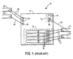
- Figure 1 shows a typical prior art power device 10 that includes an integrated circuit 11 housed within a chip carrier package.
- Integrated circuit 11 has an offline transistor 12 located in the upper right corner of the chip and an output transistor 13 located in another area of the same substrate.
- bonding wires facilitate electrical connection between the bonding pads located on IC 11 and the various pins of the chip package.
- Figure 1 shows a bonding wire 21 connected between a bonding pad 20 located on the drain electrode 14 of offline transistor 12 and pin 19 of device 10.
- wires 17 connect bonding pads 16 on drain electrode 15 of output transistor 13 to pins 18 and 19.
- wires 28 connecting bonding pads 27 to pin 29, and wire 24 connecting pad 25 to pin 23.
- bonding pads 27 and pin 29 may provide a connection to ground for IC 11, whereas pad 25 and pin 23 may connect to an external capacitor utilized for start-up purposes.
- an integrated circuit in a substrate comprising:
- a source electrode is connected to the source region of the high-voltage output transistor, the source electrode being for connection to a ground potential.
- a power device comprising:
- the integrated circuit further comprises:
- the offline transistor may be disposed adjacent the high-voltage output transistor in the substrate.
- a second source electrode may be connected to the source region of the high-voltage output transistor; and a ground pin may be connected to the second source electrode.
- the source regions of the high-voltage output and offline transistors are disposed in a common body region of the substrate.
- the drain region of the high-voltage output transistor may be disposed in a first well region, and the drain region of the offline transistor may be disposed in a second well region.
- the drain and source regions of the high-voltage output transistor are interdigitated and/or the drain and source regions of the offline transistor are interdigitated on the integrated circuit.
- the invention also relates to a circuit that includes a power device according to the invention, the circuit comprising a supply line; and a load coupled between the supply line and the first pin of the package.
- an integrated circuit fabricated on a substrate comprising:
- a first source electrode is connected to the source region of the offline transistor; and a second source electrode is connected to the source region of the high-voltage output transistor.
- the integrated circuit may also comprise a guard ring that separates the high-voltage output and offline transistors from switching circuitry.
- the integrated circuit may also comprise additional circuitry coupled to the first source electrode for driving current to an external device and the second source electrode may be connected to a ground plane.
- the offline transistor has a first breakdown voltage and the high-voltage output transistor has a second breakdown voltage, the first breakdown voltage being higher than the second breakdown voltage.
- the present invention includes a power integrated circuit that is typically housed in a package or chip carrier.
- the integrated circuit comprises a high-power output power transistor that is closely coupled with an offline transistor on the same silicon substrate.
- disposing the offline transistor adjacent to the output transistor and connecting the drain regions of the transistor pair to a common drain electrode achieves close coupling between the output transistor and the offline transistor.
- the drain electrode includes one or more bonding pad areas for connecting the output and offline transistors to a pin of the package. In a typical application, the drain electrode pin is coupled to a high-voltage supply line through a load.
- FIG. 2 is a circuit schematic diagram of the power device 30 of the present invention, wherein IC 35 is shown being coupled through an output pin 40 to a load 33.
- Load 33 is connected to supply line 31, which provides a high line voltage, V LINE .
- the drain regions of high-voltage output transistor 37 and offline transistor 36 are commonly coupled to output pin 40.
- Output transistor 37 is shown having its source and body (e.g., substrate) regions coupled to ground potential.
- the gate of high-voltage output transistor 37 is coupled to switching circuitry on IC 35, which controls the on/off state of transistor 37.
- the switching circuitry that drives the gate of output transistor 37 comprises ordinary logic that produces some sort of a digital pulse signal, e.g., a pulse width modulation signal, that controls the operation of transistor 37.
- the main function of offline transistor 36 is to provide start-up current for IC 35. Accordingly, the source region of offline transistor 36 is not grounded, as is the case for transistor 37. Instead, the body region of transistor 36 is grounded and the source of offline transistor 36 is coupled to circuitry 38 that provides output current at pin 41 of the device. The current provided at pin 41 is used to charge-up an external capacitor 42. It is appreciated that the charge-up circuitry 38 may comprise a wide variety of known analog or digital circuits useful for providing current to charge a capacitor. In certain applications, circuitry 38 may be eliminated and the source of offline transistor may be coupled directly to pin 41.
- the gate of offline transistor 36 is coupled to startup circuitry 39 in Figure 2, which comprises conventional control logic designed to turn-on transistor during the powering up of IC 35.
- circuit 39 functions by turning on transistor 36 for a time period sufficient to generate enough current to fully charge capacitor 42.
- FIG. 3 there is shown a top layout view of IC 35 in accordance with one embodiment of the present invention.
- Figure 4 is a cross-sectional side view of the closely coupled transistor pair taken through cut lines A-A', showing the doped semiconductor regions of the respective transistors.
- output transistor 37 and offline transistor 36 each comprise interdigitated source and drain regions.
- elongated source electrode fingers 46 are shown interdigitated with drain electrode fingers 47 of the high-voltage output transistor 37.
- Offline transistor 36 includes a single drain electrode finger 43 interdigitated between a pair of source fingers comprising source electrode 51.
- the offline and output transistors are disposed adjacent to one another in the same substrate. This allows both transistors to merge their respective drain electrode fingers into a common drain electrode 44.
- Figure 3 illustrates common drain electrode 44 including an area sufficiently large to accommodate the placement of bonding pads 48. Since the offline and output transistors share drain electrode 44 and bonding pads 48, the need for offline transistor to have its own bond pad is obviated in accordance with the present invention. Moreover, the common drain electrode 44 closely couples the drain voltages of the offline and output transistors, thereby allowing the larger output transistor 37 to protect offline transistor 36 from high voltage transients.
- offline transistor 36 may be configured so as to have a higher breakdown voltage as compared to output transistor 37. This may be accomplished, for example, by layout design differences wherein offline transistor 36 has a longer extended drain region and/or larger radius fingertip regions as compared to output transistor 37.
- the control circuit of the power device may function so as to turn off transistor 36 before transistor 37 in order to protect the offline transistor from high voltage transients caused by the switching off of the output transistor.
- bonding pads 48 are connected by one or more bonding wires to the high-voltage output pin 40, which is coupled to V LINE through load 33.
- bonding pads 49 are provided on the source electrode 45 at the opposite end of transistor 37. Bonding pads 49 are connected to a ground potential during operation of the power device of the present invention.
- guard ring metal trace 50 that is included in this particular embodiment for the purpose of isolating both the high-voltage output transistor 37 and offline transistor 36 from other circuitry on IC 35.
- Guard ring 50 is usually coupled to an underlying well region in the substrate. Without guard ring 50 the operation of transistors 36 and 37 might cause disruption of the switching and startup circuitry on the chip through carrier injection into the substrate. Guard ring 50 prevents additional charge carriers generated by transistors 36 & 37 from finding their way to nearby controller circuits.
- FIG. 4 illustrates the relative location of the source region, drain region and gate of each of transistors 36 & 37 in one embodiment of the present invention.
- Drain region 66 of offline transistor 36 is shown disposed in a N-well region 62, whereas drain region 74 of output transistor 37 is disposed in a separate N-well region 71.
- Drain electrode finger 43 of transistor 36 connects to drain region 66, and drain electrode finger 46 of transistor 37 connects to drain region 74. Both drain electrode fingers 43 and 46 merge into a single common drain electrode 44, as shown in Figure 3.
- output and offline transistors 36 & 37 share a common drain electrode 44, their drain diffusion regions 66 and 74 are disposed in separate N-well regions 62 and 71, respectively.
- the source diffusion region 64 of offline transistor 36 is disposed in P-substrate 60 separated from N-well 62 by a channel region 81.
- the extended drain region of transistor 36 comprises the N-type semiconductor material between N+ region 66 and the boundary of N-well 62 adjacent channel region 81.
- a thick field oxide layer 67 covers the surface of the extended drain region.
- An insulated polysilicon gate 65 is disposed over channel region 81 and slightly overlaps field oxide region 67 for field plating purposes.
- Source electrode 51 of offline transistor 36 connects with N+ source region 64 and includes an extended portion over gate 65, which acts as a field plate.
- a channel region 82 separates source region 70 from the extended drain boundary of N-well 71.
- Insulated gate 72 is disposed above channel region 82 and extends over field oxide layer 73 for field plating purposes.
- the source electrode 45 of output transistor 37 also includes a field plate portion that extends over gate 72.
- An additional P+ region 69 is shown disposed in substrate 60 next to source diffusion region 70. Source electrode 45 contacts both P+ region 69 and N+ source region 70 as a convenient way of connection both the body (i.e., substrate) and source regions of transistor 37 to the same ground potential.
- P+ region 69 is separated at the surface from N+ source region 64 by field oxide layer 68.
- an integrated circuit fabricated in a single silicon substrate includes a high-voltage output transistor having source and drain regions separated by a channel region, and a gate disposed over the channel region. Also included is an offline transistor having source and drain regions separated by a channel region and a gate disposed over the channel region of the offline transistor. A drain electrode is commonly coupled to the drain region of the high-voltage output transistor and to the drain region of the offline transistor.
Landscapes
- Metal-Oxide And Bipolar Metal-Oxide Semiconductor Integrated Circuits (AREA)
- Semiconductor Integrated Circuits (AREA)
- Logic Circuits (AREA)
- Amplifiers (AREA)
- Electronic Switches (AREA)
Abstract
Description
- The present invention relates to power integrated circuits. More specifically, the present invention relates to a high-voltage, field-effect transistors fabricated on a single silicon substrate with other transistor devices.
- A common type of integrated circuit device is a metal-oxide-semiconductor field effect transistor (MOSFET). A MOSFET is a field effect device that includes a source region, a drain region, a channel region extending between the source and drain regions, and a gate provided over the channel region. The gate includes a conductive gate structure disposed over and insulated from the channel region by a thin oxide layer.
- Power MOSFET devices are widely used for high voltage circuit applications, e.g., greater than 200 volts. Examples of traditional MOSFET device structures for power applications include U.S. Patent Nos. 5,869,875, 5,821,144, 5,760,440, and 4,748,936. Each of these devices has a source region and a drain region separated by an intermediate region. A gate structure is disposed over a thin oxide layer over the metal-oxide-semiconductor (MOS) channel of the device. In the on state, a voltage is applied to the gate to cause a conduction channel to form between the source and drain regions, thereby allowing current to flow through the device. In the off state, the voltage on the gate is sufficiently low such that no conduction channel is formed in the substrate, and thus no current flow occurs. In this condition, high voltage is supported between the drain and source regions.
- Power transistors are often designed with interdigitated source and drain regions. Such a device structure is disclosed in U.S. Patent No. 6,084,277, which is assigned to the assignee of the present application. The '277 patent teaches a lateral power MOSFET or transistor having an improved gate design that provides a large safe operating area (SOA) performance level and high current capability with moderate gate speed to suppress switching noise.
- Many power integrated circuits (ICs) contain one or more large high-voltage output transistors that control the current flow to one or more external loads. In a switch-mode power supply IC, for example, a single large high-voltage output transistor controls the current through the primary winding of a transformer and thereby controls the power delivered by the power supply. In certain applications it is also useful to include an additional high-voltage transistor on the same silicon substrate to provide a lower current coupled to, say, an external capacitor, for the purpose of assisting in the start-up of the chip or other external circuit. Such an additional high-voltage transistor is frequently referred to as an "offline" transistor, even though it resides in the same substrate as the high-voltage output transistor. (In the context of the present application, the term "offline transistor" refers to a transistor having its drain region coupled to the same external line voltage as the output transistor, but which has its gate connected to a different internal circuit node than that of the output transistor.)
- Figure 1 shows a typical prior
art power device 10 that includes an integratedcircuit 11 housed within a chip carrier package.Integrated circuit 11 has anoffline transistor 12 located in the upper right corner of the chip and anoutput transistor 13 located in another area of the same substrate. In conventional manner, bonding wires facilitate electrical connection between the bonding pads located onIC 11 and the various pins of the chip package. For example, Figure 1 shows abonding wire 21 connected between abonding pad 20 located on thedrain electrode 14 ofoffline transistor 12 andpin 19 ofdevice 10. Similarly,wires 17 connectbonding pads 16 ondrain electrode 15 ofoutput transistor 13 topins wires 28 connectingbonding pads 27 topin 29, andwire 24 connectingpad 25 topin 23. By way of example, bondingpads 27 andpin 29 may provide a connection to ground for IC 11, whereaspad 25 andpin 23 may connect to an external capacitor utilized for start-up purposes. - The prior art approach of Figure 1 has several drawbacks. First, the
offline transistor 12 is large and occupies a significant portion of silicon area.Offline transistor 12 also needs itsown bonding pad 20, which is quite large relative to the active area of the offline transistor. This greatly reduces the area efficiency ofoffline transistor 12. Secondly, the inductance of thedrain bond wires 17 & 21 decouplesoffline transistor 12 fromoutput transistor 13 during fast switching transients. This latter effect limits the ability of the output transistor to protect the offline transistor from potentially destructive high voltages that may be present atpins power device 10. - Therefore, what is needed is a power IC that overcomes the disadvantages inherent in the prior art.
- In accordance with a first aspect of the invention there is provided an integrated circuit in a substrate comprising:
- a high-voltage output transistor having source and drain regions separated by a channel region, and a gate disposed over the channel region;
- an offline transistor having source and drain regions separated by a channel region and a gate disposed over the channel region of the offline transistor;
- a drain electrode commonly coupled to the drain region of the high voltage output transistor and the drain region of the offline transistor.
-
- Preferably a source electrode is connected to the source region of the high-voltage output transistor, the source electrode being for connection to a ground potential.
- In a second aspect of the invention there is provided a power device comprising:
- an integrated circuit in a substrate that includes:
- a high-voltage output transistor having source and drain regions separated by a channel region, and a gate disposed over the channel region;
- an offline transistor having source and drain regions separated by a channel region and a gate disposed over the channel region of the offline transistor;
- a drain electrode commonly coupled to the drain region of the high-voltage output transistor and the drain region of the offline transistor; and
- a package housing the integrated circuit, the package having a first pin connected to the drain electrode.
-
- Preferably the integrated circuit further comprises:
- switching circuitry coupled to the gate of the high-voltage output transistor; and
- startup circuitry coupled to the gate of the offline transistor. A first source electrode may be connected to the source region of the offline transistor;
- additional circuitry may be coupled to the first source electrode for driving current to an external device, such as a capacitor; and
- a second pin of the package may be connected to the additional circuitry.
-
- The offline transistor may be disposed adjacent the high-voltage output transistor in the substrate. A second source electrode may be connected to the source region of the high-voltage output transistor; and a ground pin may be connected to the second source electrode.
- Preferably the source regions of the high-voltage output and offline transistors are disposed in a common body region of the substrate. The drain region of the high-voltage output transistor may be disposed in a first well region, and the drain region of the offline transistor may be disposed in a second well region. Preferably the drain and source regions of the high-voltage output transistor are interdigitated and/or the drain and source regions of the offline transistor are interdigitated on the integrated circuit.
- The invention also relates to a circuit that includes a power device according to the invention, the circuit comprising a supply line; and
a load coupled between the supply line and the first pin of the package. - In a further aspect of the invention there is provided an integrated circuit fabricated on a substrate comprising:
- a high-voltage output MOSFET having interdigitated source and drain regions separated by a channel region, and a gate disposed over the channel region;
- an offline transistor having interdigitated source and drain regions separated by a channel region and a gate disposed over the channel region of the offline transistor, the drain region of the offline transistor being disposed in a first well region and the drain region of the high-voltage transistor being disposed in a second well region, the source regions of the high-voltage output and offline transistors are disposed in a common body region of the substrate interposed between the first and second well regions;
- a drain electrode commonly coupled to the drain region of the high-voltage output transistor and the drain region of the offline transistor.
-
- Preferably a first source electrode is connected to the source region of the offline transistor; and
a second source electrode is connected to the source region of the high-voltage output transistor. - The integrated circuit may also comprise a guard ring that separates the high-voltage output and offline transistors from switching circuitry. The integrated circuit may also comprise additional circuitry coupled to the first source electrode for driving current to an external device and the second source electrode may be connected to a ground plane.
- Preferably the offline transistor has a first breakdown voltage and the high-voltage output transistor has a second breakdown voltage, the first breakdown voltage being higher than the second breakdown voltage.
- The present invention is illustrated by way of example, and not limitation, in the figures of the accompanying drawings, wherein:
- Figure 1 is a top view of a prior art power IC chip package.
- Figure 2 is a circuit schematic diagram of one embodiment of the present invention.
- Figure 3 is a top layout view of a portion of an integrated circuit according to one embodiment of the present invention.
- Figure 4 is a cross-sectional side view of the closely coupled transistor pair shown in the embodiment of Figure 3.
-
- A power device and integrated circuit with a closely coupled pair of transistors is described. In the following description, numerous specific details are set forth, such as material types, dimensions, circuit configurations, etc., in order to provide a thorough understanding of the present invention. Practitioners having ordinary skill in the IC arts will understand that the invention may be practiced without many of these details. In other instances, well-known circuit elements, techniques, and processing steps have not been described in detail to avoid obscuring the invention.
- The present invention includes a power integrated circuit that is typically housed in a package or chip carrier. The integrated circuit comprises a high-power output power transistor that is closely coupled with an offline transistor on the same silicon substrate. In one embodiment, disposing the offline transistor adjacent to the output transistor and connecting the drain regions of the transistor pair to a common drain electrode achieves close coupling between the output transistor and the offline transistor. The drain electrode includes one or more bonding pad areas for connecting the output and offline transistors to a pin of the package. In a typical application, the drain electrode pin is coupled to a high-voltage supply line through a load.
- Figure 2 is a circuit schematic diagram of the
power device 30 of the present invention, whereinIC 35 is shown being coupled through anoutput pin 40 to aload 33.Load 33, in turn, is connected to supplyline 31, which provides a high line voltage, VLINE. The drain regions of high-voltage output transistor 37 andoffline transistor 36 are commonly coupled tooutput pin 40.Output transistor 37 is shown having its source and body (e.g., substrate) regions coupled to ground potential. The gate of high-voltage output transistor 37 is coupled to switching circuitry onIC 35, which controls the on/off state oftransistor 37. Typically, the switching circuitry that drives the gate ofoutput transistor 37 comprises ordinary logic that produces some sort of a digital pulse signal, e.g., a pulse width modulation signal, that controls the operation oftransistor 37. - The main function of
offline transistor 36 is to provide start-up current forIC 35. Accordingly, the source region ofoffline transistor 36 is not grounded, as is the case fortransistor 37. Instead, the body region oftransistor 36 is grounded and the source ofoffline transistor 36 is coupled tocircuitry 38 that provides output current atpin 41 of the device. The current provided atpin 41 is used to charge-up anexternal capacitor 42. It is appreciated that the charge-upcircuitry 38 may comprise a wide variety of known analog or digital circuits useful for providing current to charge a capacitor. In certain applications,circuitry 38 may be eliminated and the source of offline transistor may be coupled directly to pin 41. - The gate of
offline transistor 36 is coupled tostartup circuitry 39 in Figure 2, which comprises conventional control logic designed to turn-on transistor during the powering up ofIC 35. Typically,circuit 39 functions by turning ontransistor 36 for a time period sufficient to generate enough current to fully chargecapacitor 42. - Referring now to Figure 3, there is shown a top layout view of
IC 35 in accordance with one embodiment of the present invention. In the embodiment of Figure 3, only the drain and source electrode metalization patterns fortransistors output transistor 37 andoffline transistor 36 each comprise interdigitated source and drain regions. For example, elongatedsource electrode fingers 46 are shown interdigitated withdrain electrode fingers 47 of the high-voltage output transistor 37.Offline transistor 36 includes a singledrain electrode finger 43 interdigitated between a pair of source fingers comprisingsource electrode 51. - Note that the offline and output transistors are disposed adjacent to one another in the same substrate. This allows both transistors to merge their respective drain electrode fingers into a
common drain electrode 44. Figure 3 illustratescommon drain electrode 44 including an area sufficiently large to accommodate the placement ofbonding pads 48. Since the offline and output transistors sharedrain electrode 44 andbonding pads 48, the need for offline transistor to have its own bond pad is obviated in accordance with the present invention. Moreover, thecommon drain electrode 44 closely couples the drain voltages of the offline and output transistors, thereby allowing thelarger output transistor 37 to protectoffline transistor 36 from high voltage transients. - In addition,
offline transistor 36 may be configured so as to have a higher breakdown voltage as compared tooutput transistor 37. This may be accomplished, for example, by layout design differences whereinoffline transistor 36 has a longer extended drain region and/or larger radius fingertip regions as compared tooutput transistor 37. In other embodiments, the control circuit of the power device may function so as to turn offtransistor 36 beforetransistor 37 in order to protect the offline transistor from high voltage transients caused by the switching off of the output transistor. - In the completely packaged power device,
bonding pads 48 are connected by one or more bonding wires to the high-voltage output pin 40, which is coupled to VLINE throughload 33. Likewise,bonding pads 49 are provided on thesource electrode 45 at the opposite end oftransistor 37.Bonding pads 49 are connected to a ground potential during operation of the power device of the present invention. - Also shown in Figure 3 is a guard
ring metal trace 50 that is included in this particular embodiment for the purpose of isolating both the high-voltage output transistor 37 andoffline transistor 36 from other circuitry onIC 35.Guard ring 50 is usually coupled to an underlying well region in the substrate. Withoutguard ring 50 the operation oftransistors Guard ring 50 prevents additional charge carriers generated bytransistors 36 & 37 from finding their way to nearby controller circuits. - Figure 4 illustrates the relative location of the source region, drain region and gate of each of
transistors 36 & 37 in one embodiment of the present invention.Drain region 66 ofoffline transistor 36 is shown disposed in a N-well region 62, whereasdrain region 74 ofoutput transistor 37 is disposed in a separate N-well region 71.Drain electrode finger 43 oftransistor 36 connects to drainregion 66, and drainelectrode finger 46 oftransistor 37 connects to drainregion 74. Bothdrain electrode fingers common drain electrode 44, as shown in Figure 3. Thus, while output andoffline transistors 36 & 37 share acommon drain electrode 44, theirdrain diffusion regions well regions - The
source diffusion region 64 ofoffline transistor 36 is disposed in P-substrate 60 separated from N-well 62 by achannel region 81. The extended drain region oftransistor 36 comprises the N-type semiconductor material betweenN+ region 66 and the boundary of N-well 62adjacent channel region 81. A thickfield oxide layer 67 covers the surface of the extended drain region. Aninsulated polysilicon gate 65 is disposed overchannel region 81 and slightly overlapsfield oxide region 67 for field plating purposes.Source electrode 51 ofoffline transistor 36 connects withN+ source region 64 and includes an extended portion overgate 65, which acts as a field plate. - The same basic transistor structure is shown for
output transistor 37. For example, achannel region 82 separates sourceregion 70 from the extended drain boundary of N-well 71. Insulatedgate 72 is disposed abovechannel region 82 and extends overfield oxide layer 73 for field plating purposes. The source electrode 45 ofoutput transistor 37 also includes a field plate portion that extends overgate 72. Anadditional P+ region 69 is shown disposed insubstrate 60 next to sourcediffusion region 70.Source electrode 45 contacts bothP+ region 69 andN+ source region 70 as a convenient way of connection both the body (i.e., substrate) and source regions oftransistor 37 to the same ground potential. Becausechannel regions respective transistors substrate 60, the connection toP+ region 69 also grounds the body region oftransistor 36.P+ region 69 is separated at the surface fromN+ source region 64 byfield oxide layer 68. - Thus there is provided an integrated circuit fabricated in a single silicon substrate includes a high-voltage output transistor having source and drain regions separated by a channel region, and a gate disposed over the channel region. Also included is an offline transistor having source and drain regions separated by a channel region and a gate disposed over the channel region of the offline transistor. A drain electrode is commonly coupled to the drain region of the high-voltage output transistor and to the drain region of the offline transistor.
Claims (17)
- An integrated circuit in a substrate comprising:a high-voltage output transistor having source and drain regions separated by a channel region, and a gate disposed over the channel region;an offline transistor having source and drain regions separated by a channel region and a gate disposed over the channel region of the offline transistor;a drain electrode commonly coupled to the drain region of the high-voltage output transistor and the drain region of the offline transistor.
- An integrated circuit according to claim 1 further comprising:switching circuitry coupled to the gate of the high-voltage output transistor; andstartup circuitry coupled to the gate of the offline transistor.
- An integrated circuit according to claim 2 further comprising a guard ring that separates the high-voltage output and offline transistors from the switching circuitry.
- An integrated circuit according to claim 1, 2 or 3 further comprising:a first source electrode connected to the source region of the offline transistor.
- An integrated circuit according to claim 4 further comprising:additional circuitry coupled to the first source electrode for driving current to an external device.
- An integrated circuit according to claim 4 or 5 further comprising:a second source electrode connected to the source region of the high-voltage output transistor.
- An integrated circuit according to claim 6 wherein the second source electrode is connectable to a ground plane.
- An integrated circuit according to any preceding claim wherein the offline transistor is disposed adjacent the high-voltage output transistor in the substrate.
- An integrated circuit according to any preceding claim wherein the offline transistor has a first breakdown voltage and the high-voltage output transistor has a second breakdown voltage, the first breakdown voltage being higher than the second breakdown voltage.
- An integrated circuit according to any preceding claim wherein the source regions of the high-voltage output and offline transistors are disposed in a common body region.
- An integrated circuit according to any preceding claim wherein the drain region of the high-voltage output transistor is disposed in a first well region, and the drain region of the offline transistor is disposed in a second well region.
- An integrated circuit according to claims 10 and 11 wherein the body region is a region of the substrate interposed between the first and second well regions.
- An integrated circuit according to any preceding claim wherein the drain and source regions of the high-voltage output transistor and/or the offline transistor are interdigitated.
- A power device comprising:an integrated circuit according to any preceding claim and a package housing the integrated circuit, the package having a first pin connected to the drain electrode.
- The power device according to claim 14 where dependent on claim 5 further comprising:a second pin of the package connected to the additional circuitry.
- The power device according to claim 15 wherein the external device comprises a capacitor.
- A circuit that includes the power device according to any of claims 14 to 16, the circuit comprising:a supply line; anda load coupled between the supply line and the first pin of the package.
Priority Applications (1)
| Application Number | Priority Date | Filing Date | Title |
|---|---|---|---|
| EP20090162684 EP2093799A3 (en) | 2001-11-02 | 2002-08-16 | Integrated circuit with closely coupled high-voltage output and offline transistor pair |
Applications Claiming Priority (2)
| Application Number | Priority Date | Filing Date | Title |
|---|---|---|---|
| US53538 | 2001-11-02 | ||
| US10/053,538 US6552597B1 (en) | 2001-11-02 | 2001-11-02 | Integrated circuit with closely coupled high voltage output and offline transistor pair |
Related Child Applications (1)
| Application Number | Title | Priority Date | Filing Date |
|---|---|---|---|
| EP20090162684 Division EP2093799A3 (en) | 2001-11-02 | 2002-08-16 | Integrated circuit with closely coupled high-voltage output and offline transistor pair |
Publications (3)
| Publication Number | Publication Date |
|---|---|
| EP1309006A2 true EP1309006A2 (en) | 2003-05-07 |
| EP1309006A3 EP1309006A3 (en) | 2007-08-22 |
| EP1309006B1 EP1309006B1 (en) | 2009-06-17 |
Family
ID=21984966
Family Applications (2)
| Application Number | Title | Priority Date | Filing Date |
|---|---|---|---|
| EP20020255727 Expired - Lifetime EP1309006B1 (en) | 2001-11-02 | 2002-08-16 | Integrated circuit with closely coupled high-voltage output and offline transistor pair. |
| EP20090162684 Withdrawn EP2093799A3 (en) | 2001-11-02 | 2002-08-16 | Integrated circuit with closely coupled high-voltage output and offline transistor pair |
Family Applications After (1)
| Application Number | Title | Priority Date | Filing Date |
|---|---|---|---|
| EP20090162684 Withdrawn EP2093799A3 (en) | 2001-11-02 | 2002-08-16 | Integrated circuit with closely coupled high-voltage output and offline transistor pair |
Country Status (5)
| Country | Link |
|---|---|
| US (2) | US6552597B1 (en) |
| EP (2) | EP1309006B1 (en) |
| JP (1) | JP4125567B2 (en) |
| AT (1) | ATE434267T1 (en) |
| DE (1) | DE60232635D1 (en) |
Families Citing this family (34)
| Publication number | Priority date | Publication date | Assignee | Title |
|---|---|---|---|---|
| US7786533B2 (en) * | 2001-09-07 | 2010-08-31 | Power Integrations, Inc. | High-voltage vertical transistor with edge termination structure |
| US6573558B2 (en) * | 2001-09-07 | 2003-06-03 | Power Integrations, Inc. | High-voltage vertical transistor with a multi-layered extended drain structure |
| US7221011B2 (en) * | 2001-09-07 | 2007-05-22 | Power Integrations, Inc. | High-voltage vertical transistor with a multi-gradient drain doping profile |
| US6635544B2 (en) * | 2001-09-07 | 2003-10-21 | Power Intergrations, Inc. | Method of fabricating a high-voltage transistor with a multi-layered extended drain structure |
| US6552597B1 (en) * | 2001-11-02 | 2003-04-22 | Power Integrations, Inc. | Integrated circuit with closely coupled high voltage output and offline transistor pair |
| US7719054B2 (en) * | 2006-05-31 | 2010-05-18 | Advanced Analogic Technologies, Inc. | High-voltage lateral DMOS device |
| US7135748B2 (en) * | 2004-10-26 | 2006-11-14 | Power Integrations, Inc. | Integrated circuit with multi-length output transistor segment |
| US20060086974A1 (en) * | 2004-10-26 | 2006-04-27 | Power Integrations, Inc. | Integrated circuit with multi-length power transistor segments |
| US8093621B2 (en) | 2008-12-23 | 2012-01-10 | Power Integrations, Inc. | VTS insulated gate bipolar transistor |
| US7557406B2 (en) * | 2007-02-16 | 2009-07-07 | Power Integrations, Inc. | Segmented pillar layout for a high-voltage vertical transistor |
| US7859037B2 (en) | 2007-02-16 | 2010-12-28 | Power Integrations, Inc. | Checkerboarded high-voltage vertical transistor layout |
| US7468536B2 (en) | 2007-02-16 | 2008-12-23 | Power Integrations, Inc. | Gate metal routing for transistor with checkerboarded layout |
| US7595523B2 (en) | 2007-02-16 | 2009-09-29 | Power Integrations, Inc. | Gate pullback at ends of high-voltage vertical transistor structure |
| US8653583B2 (en) * | 2007-02-16 | 2014-02-18 | Power Integrations, Inc. | Sensing FET integrated with a high-voltage transistor |
| US7875962B2 (en) * | 2007-10-15 | 2011-01-25 | Power Integrations, Inc. | Package for a power semiconductor device |
| US7964912B2 (en) | 2008-09-18 | 2011-06-21 | Power Integrations, Inc. | High-voltage vertical transistor with a varied width silicon pillar |
| US7871882B2 (en) | 2008-12-20 | 2011-01-18 | Power Integrations, Inc. | Method of fabricating a deep trench insulated gate bipolar transistor |
| US20100155831A1 (en) * | 2008-12-20 | 2010-06-24 | Power Integrations, Inc. | Deep trench insulated gate bipolar transistor |
| US8115457B2 (en) | 2009-07-31 | 2012-02-14 | Power Integrations, Inc. | Method and apparatus for implementing a power converter input terminal voltage discharge circuit |
| US8207455B2 (en) * | 2009-07-31 | 2012-06-26 | Power Integrations, Inc. | Power semiconductor package with bottom surface protrusions |
| US8207577B2 (en) * | 2009-09-29 | 2012-06-26 | Power Integrations, Inc. | High-voltage transistor structure with reduced gate capacitance |
| US7893754B1 (en) | 2009-10-02 | 2011-02-22 | Power Integrations, Inc. | Temperature independent reference circuit |
| US8634218B2 (en) | 2009-10-06 | 2014-01-21 | Power Integrations, Inc. | Monolithic AC/DC converter for generating DC supply voltage |
| US8310845B2 (en) * | 2010-02-10 | 2012-11-13 | Power Integrations, Inc. | Power supply circuit with a control terminal for different functional modes of operation |
| US8709883B2 (en) * | 2011-08-19 | 2014-04-29 | Freescale Semiconductor, Inc. | Implant for performance enhancement of selected transistors in an integrated circuit |
| US8653600B2 (en) | 2012-06-01 | 2014-02-18 | Power Integrations, Inc. | High-voltage monolithic schottky device structure |
| US9455621B2 (en) | 2013-08-28 | 2016-09-27 | Power Integrations, Inc. | Controller IC with zero-crossing detector and capacitor discharge switching element |
| US9543396B2 (en) | 2013-12-13 | 2017-01-10 | Power Integrations, Inc. | Vertical transistor device structure with cylindrically-shaped regions |
| US10325988B2 (en) | 2013-12-13 | 2019-06-18 | Power Integrations, Inc. | Vertical transistor device structure with cylindrically-shaped field plates |
| US9667154B2 (en) | 2015-09-18 | 2017-05-30 | Power Integrations, Inc. | Demand-controlled, low standby power linear shunt regulator |
| US9602009B1 (en) | 2015-12-08 | 2017-03-21 | Power Integrations, Inc. | Low voltage, closed loop controlled energy storage circuit |
| US9629218B1 (en) | 2015-12-28 | 2017-04-18 | Power Integrations, Inc. | Thermal protection for LED bleeder in fault condition |
| CN105895667B (en) * | 2015-12-28 | 2019-07-23 | 苏州能讯高能半导体有限公司 | A kind of semiconductor devices and its manufacturing method |
| CN105742364A (en) * | 2016-04-12 | 2016-07-06 | 中山大学 | MOS transistor capable of restraining photoinduced leakage current in active channel region, and application of MOS transistor |
Citations (3)
| Publication number | Priority date | Publication date | Assignee | Title |
|---|---|---|---|---|
| US4939566A (en) | 1987-10-30 | 1990-07-03 | North American Philips Corporation | Semiconductor switch with parallel DMOS and IGT |
| US4962349A (en) | 1988-01-29 | 1990-10-09 | U.S. Philips Corporation | Battery operated power supply with low voltage start circuit |
| US6084277A (en) | 1999-02-18 | 2000-07-04 | Power Integrations, Inc. | Lateral power MOSFET with improved gate design |
Family Cites Families (21)
| Publication number | Priority date | Publication date | Assignee | Title |
|---|---|---|---|---|
| US5023678A (en) * | 1987-05-27 | 1991-06-11 | International Rectifier Corporation | High power MOSFET and integrated control circuit therefor for high-side switch application |
| US4890146A (en) * | 1987-12-16 | 1989-12-26 | Siliconix Incorporated | High voltage level shift semiconductor device |
| US4924112A (en) * | 1988-10-31 | 1990-05-08 | Motorola Inc. | Microprocessor having high current drive and feedback for temperature control |
| JP2856853B2 (en) * | 1990-07-03 | 1999-02-10 | 株式会社東芝 | Semiconductor device |
| US5063307A (en) * | 1990-09-20 | 1991-11-05 | Ixys Corporation | Insulated gate transistor devices with temperature and current sensor |
| US5334880A (en) * | 1991-04-30 | 1994-08-02 | International Business Machines Corporation | Low voltage programmable storage element |
| US5311462A (en) * | 1991-12-19 | 1994-05-10 | Intel Corporation | Physical placement of content addressable memories |
| US5338978A (en) * | 1993-02-10 | 1994-08-16 | National Semiconductor Corporation | Full swing power down buffer circuit with multiple power supply isolation |
| JPH07264042A (en) * | 1994-03-17 | 1995-10-13 | Fujitsu Ltd | High speed interface circuit |
| US5672992A (en) * | 1995-04-11 | 1997-09-30 | International Rectifier Corporation | Charge pump circuit for high side switch |
| JP3509318B2 (en) * | 1995-08-09 | 2004-03-22 | 日産自動車株式会社 | Power Bipolar Transistor Controller |
| JP3618424B2 (en) * | 1995-09-07 | 2005-02-09 | エイ・アイ・エル株式会社 | Low power logic circuit |
| JPH09214315A (en) * | 1996-02-08 | 1997-08-15 | Toshiba Corp | Output buffer, semiconductor integrated circuit, and method for adjusting output buffer drive capability |
| US5748025A (en) * | 1996-03-29 | 1998-05-05 | Intel Corporation | Method and apparatus for providing high voltage with a low voltage CMOS integrated circuit |
| US5814884C1 (en) * | 1996-10-24 | 2002-01-29 | Int Rectifier Corp | Commonly housed diverse semiconductor die |
| US6316807B1 (en) * | 1997-12-05 | 2001-11-13 | Naoto Fujishima | Low on-resistance trench lateral MISFET with better switching characteristics and method for manufacturing same |
| GB2341272B (en) * | 1998-09-03 | 2003-08-20 | Ericsson Telefon Ab L M | High voltage shield |
| US6198308B1 (en) * | 1999-03-30 | 2001-03-06 | Fairchild Semiconductor Corp. | Circuit for dynamic switching of a buffer threshold |
| US6586283B2 (en) * | 2000-03-30 | 2003-07-01 | Agilent Technologies, Inc. | Apparatus and method for protecting integrated circuit charge storage elements from photo-induced currents |
| JP4024990B2 (en) * | 2000-04-28 | 2007-12-19 | 株式会社ルネサステクノロジ | Semiconductor device |
| US6552597B1 (en) * | 2001-11-02 | 2003-04-22 | Power Integrations, Inc. | Integrated circuit with closely coupled high voltage output and offline transistor pair |
-
2001
- 2001-11-02 US US10/053,538 patent/US6552597B1/en not_active Expired - Lifetime
-
2002
- 2002-07-31 JP JP2002258267A patent/JP4125567B2/en not_active Expired - Fee Related
- 2002-08-16 EP EP20020255727 patent/EP1309006B1/en not_active Expired - Lifetime
- 2002-08-16 EP EP20090162684 patent/EP2093799A3/en not_active Withdrawn
- 2002-08-16 DE DE60232635T patent/DE60232635D1/en not_active Expired - Lifetime
- 2002-08-16 AT AT02255727T patent/ATE434267T1/en not_active IP Right Cessation
-
2003
- 2003-01-30 US US10/354,788 patent/US6734714B2/en not_active Expired - Fee Related
Patent Citations (3)
| Publication number | Priority date | Publication date | Assignee | Title |
|---|---|---|---|---|
| US4939566A (en) | 1987-10-30 | 1990-07-03 | North American Philips Corporation | Semiconductor switch with parallel DMOS and IGT |
| US4962349A (en) | 1988-01-29 | 1990-10-09 | U.S. Philips Corporation | Battery operated power supply with low voltage start circuit |
| US6084277A (en) | 1999-02-18 | 2000-07-04 | Power Integrations, Inc. | Lateral power MOSFET with improved gate design |
Also Published As
| Publication number | Publication date |
|---|---|
| EP2093799A3 (en) | 2010-03-10 |
| EP1309006B1 (en) | 2009-06-17 |
| EP2093799A2 (en) | 2009-08-26 |
| US6734714B2 (en) | 2004-05-11 |
| ATE434267T1 (en) | 2009-07-15 |
| US20030112052A1 (en) | 2003-06-19 |
| EP1309006A3 (en) | 2007-08-22 |
| JP4125567B2 (en) | 2008-07-30 |
| JP2003264241A (en) | 2003-09-19 |
| US6552597B1 (en) | 2003-04-22 |
| DE60232635D1 (en) | 2009-07-30 |
Similar Documents
| Publication | Publication Date | Title |
|---|---|---|
| US6552597B1 (en) | Integrated circuit with closely coupled high voltage output and offline transistor pair | |
| US7238991B2 (en) | Semiconductor device with improved protection from electrostatic discharge | |
| US10446687B2 (en) | Integrated circuit connection arrangement for minimizing crosstalk | |
| US20020179945A1 (en) | Power semiconductor device | |
| JPH07202126A (en) | Semiconductor device | |
| US6479869B1 (en) | Semiconductor device with enhanced protection from electrostatic breakdown | |
| US7812402B2 (en) | Semiconductor device | |
| JP2006509360A (en) | Integrated half-bridge power circuit | |
| US20080128828A1 (en) | Semiconductor device | |
| US6411480B1 (en) | Substrate pumped ESD network with trench structure | |
| US6608744B1 (en) | SOI CMOS input protection circuit with open-drain configuration | |
| JP2009206284A (en) | Semiconductor device | |
| EP1325519B1 (en) | Semiconductor apparatus with improved ESD withstanding voltage | |
| JP2954854B2 (en) | Integrated circuit chip | |
| US6894351B2 (en) | Semiconductor device for electrostatic protection | |
| US20020070408A1 (en) | Electrostatic discharge protection for mosfets | |
| US5604369A (en) | ESD protection device for high voltage CMOS applications | |
| JPS61296770A (en) | Insulated gate field effect semiconductor device | |
| JP3444263B2 (en) | Insulated gate semiconductor device with built-in control circuit | |
| US6809393B1 (en) | Level shifter | |
| KR100312467B1 (en) | Semiconductor ic device | |
| JP2970826B2 (en) | Protection circuit built-in IC and display device driving IC | |
| JPH0553074B2 (en) | ||
| US6515332B1 (en) | Insulated-gate field-effect semiconductor device | |
| JPH0430571A (en) | Semiconductor integrated circuit for high dielectric strength type drive |
Legal Events
| Date | Code | Title | Description |
|---|---|---|---|
| PUAI | Public reference made under article 153(3) epc to a published international application that has entered the european phase |
Free format text: ORIGINAL CODE: 0009012 |
|
| AK | Designated contracting states |
Designated state(s): AT BE BG CH CY CZ DE DK EE ES FI FR GB GR IE IT LI LU MC NL PT SE SK TR |
|
| AX | Request for extension of the european patent |
Extension state: AL LT LV MK RO SI |
|
| PUAL | Search report despatched |
Free format text: ORIGINAL CODE: 0009013 |
|
| AK | Designated contracting states |
Kind code of ref document: A3 Designated state(s): AT BE BG CH CY CZ DE DK EE ES FI FR GB GR IE IT LI LU MC NL PT SE SK TR |
|
| AX | Request for extension of the european patent |
Extension state: AL LT LV MK RO SI |
|
| 17P | Request for examination filed |
Effective date: 20070906 |
|
| 17Q | First examination report despatched |
Effective date: 20071010 |
|
| AKX | Designation fees paid |
Designated state(s): AT BE BG CH CY CZ DE DK EE ES FI FR GB GR IE IT LI LU MC NL PT SE SK TR |
|
| RAP3 | Party data changed (applicant data changed or rights of an application transferred) |
Owner name: POWER INTEGRATIONS, INC. |
|
| GRAP | Despatch of communication of intention to grant a patent |
Free format text: ORIGINAL CODE: EPIDOSNIGR1 |
|
| GRAS | Grant fee paid |
Free format text: ORIGINAL CODE: EPIDOSNIGR3 |
|
| GRAA | (expected) grant |
Free format text: ORIGINAL CODE: 0009210 |
|
| AK | Designated contracting states |
Kind code of ref document: B1 Designated state(s): AT BE BG CH CY CZ DE DK EE ES FI FR GB GR IE IT LI LU MC NL PT SE SK TR |
|
| REG | Reference to a national code |
Ref country code: GB Ref legal event code: FG4D |
|
| REG | Reference to a national code |
Ref country code: CH Ref legal event code: EP |
|
| REG | Reference to a national code |
Ref country code: IE Ref legal event code: FG4D |
|
| REF | Corresponds to: |
Ref document number: 60232635 Country of ref document: DE Date of ref document: 20090730 Kind code of ref document: P |
|
| REG | Reference to a national code |
Ref country code: SE Ref legal event code: TRGR |
|
| PG25 | Lapsed in a contracting state [announced via postgrant information from national office to epo] |
Ref country code: AT Free format text: LAPSE BECAUSE OF FAILURE TO SUBMIT A TRANSLATION OF THE DESCRIPTION OR TO PAY THE FEE WITHIN THE PRESCRIBED TIME-LIMIT Effective date: 20090617 Ref country code: FI Free format text: LAPSE BECAUSE OF FAILURE TO SUBMIT A TRANSLATION OF THE DESCRIPTION OR TO PAY THE FEE WITHIN THE PRESCRIBED TIME-LIMIT Effective date: 20090617 |
|
| PG25 | Lapsed in a contracting state [announced via postgrant information from national office to epo] |
Ref country code: EE Free format text: LAPSE BECAUSE OF FAILURE TO SUBMIT A TRANSLATION OF THE DESCRIPTION OR TO PAY THE FEE WITHIN THE PRESCRIBED TIME-LIMIT Effective date: 20090617 Ref country code: ES Free format text: LAPSE BECAUSE OF FAILURE TO SUBMIT A TRANSLATION OF THE DESCRIPTION OR TO PAY THE FEE WITHIN THE PRESCRIBED TIME-LIMIT Effective date: 20090928 Ref country code: CZ Free format text: LAPSE BECAUSE OF FAILURE TO SUBMIT A TRANSLATION OF THE DESCRIPTION OR TO PAY THE FEE WITHIN THE PRESCRIBED TIME-LIMIT Effective date: 20090617 |
|
| PG25 | Lapsed in a contracting state [announced via postgrant information from national office to epo] |
Ref country code: SK Free format text: LAPSE BECAUSE OF FAILURE TO SUBMIT A TRANSLATION OF THE DESCRIPTION OR TO PAY THE FEE WITHIN THE PRESCRIBED TIME-LIMIT Effective date: 20090617 Ref country code: BE Free format text: LAPSE BECAUSE OF FAILURE TO SUBMIT A TRANSLATION OF THE DESCRIPTION OR TO PAY THE FEE WITHIN THE PRESCRIBED TIME-LIMIT Effective date: 20090617 |
|
| PG25 | Lapsed in a contracting state [announced via postgrant information from national office to epo] |
Ref country code: BG Free format text: LAPSE BECAUSE OF FAILURE TO SUBMIT A TRANSLATION OF THE DESCRIPTION OR TO PAY THE FEE WITHIN THE PRESCRIBED TIME-LIMIT Effective date: 20090917 Ref country code: MC Free format text: LAPSE BECAUSE OF NON-PAYMENT OF DUE FEES Effective date: 20090831 Ref country code: PT Free format text: LAPSE BECAUSE OF FAILURE TO SUBMIT A TRANSLATION OF THE DESCRIPTION OR TO PAY THE FEE WITHIN THE PRESCRIBED TIME-LIMIT Effective date: 20091017 |
|
| REG | Reference to a national code |
Ref country code: CH Ref legal event code: PL |
|
| PLBE | No opposition filed within time limit |
Free format text: ORIGINAL CODE: 0009261 |
|
| STAA | Information on the status of an ep patent application or granted ep patent |
Free format text: STATUS: NO OPPOSITION FILED WITHIN TIME LIMIT |
|
| PG25 | Lapsed in a contracting state [announced via postgrant information from national office to epo] |
Ref country code: LI Free format text: LAPSE BECAUSE OF NON-PAYMENT OF DUE FEES Effective date: 20090831 Ref country code: CH Free format text: LAPSE BECAUSE OF NON-PAYMENT OF DUE FEES Effective date: 20090831 Ref country code: DK Free format text: LAPSE BECAUSE OF FAILURE TO SUBMIT A TRANSLATION OF THE DESCRIPTION OR TO PAY THE FEE WITHIN THE PRESCRIBED TIME-LIMIT Effective date: 20090617 |
|
| 26N | No opposition filed |
Effective date: 20100318 |
|
| PG25 | Lapsed in a contracting state [announced via postgrant information from national office to epo] |
Ref country code: IE Free format text: LAPSE BECAUSE OF NON-PAYMENT OF DUE FEES Effective date: 20090816 |
|
| PG25 | Lapsed in a contracting state [announced via postgrant information from national office to epo] |
Ref country code: GR Free format text: LAPSE BECAUSE OF FAILURE TO SUBMIT A TRANSLATION OF THE DESCRIPTION OR TO PAY THE FEE WITHIN THE PRESCRIBED TIME-LIMIT Effective date: 20090918 |
|
| PG25 | Lapsed in a contracting state [announced via postgrant information from national office to epo] |
Ref country code: LU Free format text: LAPSE BECAUSE OF NON-PAYMENT OF DUE FEES Effective date: 20090816 |
|
| PG25 | Lapsed in a contracting state [announced via postgrant information from national office to epo] |
Ref country code: TR Free format text: LAPSE BECAUSE OF FAILURE TO SUBMIT A TRANSLATION OF THE DESCRIPTION OR TO PAY THE FEE WITHIN THE PRESCRIBED TIME-LIMIT Effective date: 20090617 |
|
| PG25 | Lapsed in a contracting state [announced via postgrant information from national office to epo] |
Ref country code: CY Free format text: LAPSE BECAUSE OF FAILURE TO SUBMIT A TRANSLATION OF THE DESCRIPTION OR TO PAY THE FEE WITHIN THE PRESCRIBED TIME-LIMIT Effective date: 20090617 |
|
| PGFP | Annual fee paid to national office [announced via postgrant information from national office to epo] |
Ref country code: NL Payment date: 20130826 Year of fee payment: 12 Ref country code: SE Payment date: 20130828 Year of fee payment: 12 Ref country code: DE Payment date: 20130828 Year of fee payment: 12 |
|
| PGFP | Annual fee paid to national office [announced via postgrant information from national office to epo] |
Ref country code: FR Payment date: 20130819 Year of fee payment: 12 Ref country code: GB Payment date: 20130827 Year of fee payment: 12 |
|
| PGFP | Annual fee paid to national office [announced via postgrant information from national office to epo] |
Ref country code: IT Payment date: 20130823 Year of fee payment: 12 |
|
| REG | Reference to a national code |
Ref country code: DE Ref legal event code: R119 Ref document number: 60232635 Country of ref document: DE |
|
| REG | Reference to a national code |
Ref country code: NL Ref legal event code: V1 Effective date: 20150301 |
|
| REG | Reference to a national code |
Ref country code: SE Ref legal event code: EUG |
|
| GBPC | Gb: european patent ceased through non-payment of renewal fee |
Effective date: 20140816 |
|
| PG25 | Lapsed in a contracting state [announced via postgrant information from national office to epo] |
Ref country code: NL Free format text: LAPSE BECAUSE OF NON-PAYMENT OF DUE FEES Effective date: 20150301 Ref country code: IT Free format text: LAPSE BECAUSE OF NON-PAYMENT OF DUE FEES Effective date: 20140816 |
|
| REG | Reference to a national code |
Ref country code: DE Ref legal event code: R119 Ref document number: 60232635 Country of ref document: DE Effective date: 20150303 |
|
| PG25 | Lapsed in a contracting state [announced via postgrant information from national office to epo] |
Ref country code: SE Free format text: LAPSE BECAUSE OF NON-PAYMENT OF DUE FEES Effective date: 20140817 |
|
| REG | Reference to a national code |
Ref country code: FR Ref legal event code: ST Effective date: 20150430 |
|
| PG25 | Lapsed in a contracting state [announced via postgrant information from national office to epo] |
Ref country code: DE Free format text: LAPSE BECAUSE OF NON-PAYMENT OF DUE FEES Effective date: 20150303 Ref country code: GB Free format text: LAPSE BECAUSE OF NON-PAYMENT OF DUE FEES Effective date: 20140816 |
|
| PG25 | Lapsed in a contracting state [announced via postgrant information from national office to epo] |
Ref country code: FR Free format text: LAPSE BECAUSE OF NON-PAYMENT OF DUE FEES Effective date: 20140901 |