EP1308990A2 - Ferroelectric capacitor and a semiconductor device - Google Patents
Ferroelectric capacitor and a semiconductor device Download PDFInfo
- Publication number
- EP1308990A2 EP1308990A2 EP02007739A EP02007739A EP1308990A2 EP 1308990 A2 EP1308990 A2 EP 1308990A2 EP 02007739 A EP02007739 A EP 02007739A EP 02007739 A EP02007739 A EP 02007739A EP 1308990 A2 EP1308990 A2 EP 1308990A2
- Authority
- EP
- European Patent Office
- Prior art keywords
- film
- ferroelectric
- ferroelectric capacitor
- pzt
- ferroelectric film
- Prior art date
- Legal status (The legal status is an assumption and is not a legal conclusion. Google has not performed a legal analysis and makes no representation as to the accuracy of the status listed.)
- Granted
Links
Images







Classifications
-
- H—ELECTRICITY
- H10—SEMICONDUCTOR DEVICES; ELECTRIC SOLID-STATE DEVICES NOT OTHERWISE PROVIDED FOR
- H10B—ELECTRONIC MEMORY DEVICES
- H10B53/00—Ferroelectric RAM [FeRAM] devices comprising ferroelectric memory capacitors
-
- H—ELECTRICITY
- H10—SEMICONDUCTOR DEVICES; ELECTRIC SOLID-STATE DEVICES NOT OTHERWISE PROVIDED FOR
- H10D—INORGANIC ELECTRIC SEMICONDUCTOR DEVICES
- H10D84/00—Integrated devices formed in or on semiconductor substrates that comprise only semiconducting layers, e.g. on Si wafers or on GaAs-on-Si wafers
- H10D84/80—Integrated devices formed in or on semiconductor substrates that comprise only semiconducting layers, e.g. on Si wafers or on GaAs-on-Si wafers characterised by the integration of at least one component covered by groups H10D12/00 or H10D30/00, e.g. integration of IGFETs
-
- H—ELECTRICITY
- H10—SEMICONDUCTOR DEVICES; ELECTRIC SOLID-STATE DEVICES NOT OTHERWISE PROVIDED FOR
- H10B—ELECTRONIC MEMORY DEVICES
- H10B53/00—Ferroelectric RAM [FeRAM] devices comprising ferroelectric memory capacitors
- H10B53/30—Ferroelectric RAM [FeRAM] devices comprising ferroelectric memory capacitors characterised by the memory core region
-
- H—ELECTRICITY
- H10—SEMICONDUCTOR DEVICES; ELECTRIC SOLID-STATE DEVICES NOT OTHERWISE PROVIDED FOR
- H10D—INORGANIC ELECTRIC SEMICONDUCTOR DEVICES
- H10D1/00—Resistors, capacitors or inductors
- H10D1/60—Capacitors
- H10D1/68—Capacitors having no potential barriers
- H10D1/682—Capacitors having no potential barriers having dielectrics comprising perovskite structures
- H10D1/684—Capacitors having no potential barriers having dielectrics comprising perovskite structures the dielectrics comprising multiple layers, e.g. comprising buffer layers, seed layers or gradient layers
Definitions
- the present invention relates to a semiconductor device and particularly relates to a semiconductor device having a ferroelectric capacitor.
- Non-volatile magnetic disk devices are commonly used as large-scale auxiliary storage devices for storing programs and data.
- magnetic disk devices are bulky, vulnerable to mechanical shocks and have a large consumption power.
- a further drawback of magnetic devices is a slow access speed during information read/write operations.
- EEPROMs or flash memories that store information by accumulating electric charges on floating gate electrodes are often used as nonvolatile auxiliary storage devices.
- flash memories have a cell structure similar to DRAMs and can be formed at a large integration density. Therefore, flash memories are becoming of an interest as large-scale memory devices that are comparable to magnetic disk devices.
- FeRAM ferroelectric memory device
- Such FeRAM has a structure similar to that of the DRAM in that each memory cell transistor is provided as a single MOSFET. Further, a dielectric film in the memory cell capacitor is replaced by a ferroelectric material such as PZT (Pb(Zr,Ti)O 3 ) or PLZT ((Pb,La)(Zr,Ti)O 3 ) and further by SBT(SrBi 2 Ta 2 O 3 ).
- PZT Pb(Zr,Ti)O 3
- PLZT PLZT
- SBT SrBi 2 Ta 2 O 3
- the ferroelectric semiconductor memory device controls the spontaneous polarization of the ferroelectric capacitor by applying electric fields, so that a writing speed becomes faster by a factor of 1000 or more as compared to an EEPROM or a flash-memory in which information is written by injecting hot electrons into the floating gate through the tunneling insulation film.
- the FeRAM is advantageous in that the power consumption is reduced to about 1/10 that of an EEPROM or a flash-memory. Further, since a tunneling insulation film is no required, the FeRAM has an increased lifetime and can perform writing operations of about one hundred thousand times that of a flash-memory device.
- Fig. 1 shows the construction of a conventional FeRAM 10.
- the FeRAM 10 is constructed on a p-type Si-substrate 11 and is formed on a p-type well 11A having an active region defined by a field oxide film 12.
- a gate electrode 13 is formed in correspondence to a word line of the FeRAM via a gate oxide film that is not shown in the figure.
- n + -type diffusion regions 11B and 11C are formed in the substrate 11 on both sides of the gate electrode 13 to serve as a source region and a drain region, respectively, of the memory cell transistor.
- a channel region is formed in the p-type well 11A at a position between the diffusion regions 11B and 11C.
- the gate electrode 13 is covered by a CVD oxide film 14 that covers the surface of the Si substrate 11 in correspondence to the active regions.
- a ferroelectric capacitor C including a lower electrode 15, a ferroelectric film 16 such as a PZT film formed on the lower electrode 16 and an upper electrode 17 formed on the ferroelectric film 16 is formed on the CVD oxide film 14.
- the ferroelectric capacitor C is covered with an insulation film 18 such as a CVD oxide film.
- the upper electrode 17 is electrically connected to the diffusion region 11B via a local interconnection pattern 19A that contacts the upper electrode 17 at a contact hole formed in the insulation film 18 and contacts the diffusion region 11B at a contact hole formed in the insulation films 18 and 14.
- the diffusion region 11C is electrically connected to an electrode 19B that forms a bit-line of the FeRAM 10.
- the entire surface of the thus-formed FeRAM 10 is protected by a protection insulation film 20.
- the lower electrode 15 is often made of a Ti/Pt stacked film and the ferroelectric film 16 provided on the lower electrode 15 is made of a PZT film.
- the Pt film forming the lower electrode 15 is mainly formed of Pt polycrystals oriented in the ⁇ 111> direction. Therefore the orientation of the ferroelectric film 16 formed on the Ti/Pt stacked film is dominated by the orientation of the lower electrode and, as a result, is mainly oriented in the ⁇ 111> direction. That is to say, it is known that such a ferroelectric capacitor has a so-called (111) orientation (see J. Appl. Phys, vol. 70, No. 1, 1991, pp. 382-388).
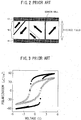
- Fig. 2 is a schematic diagram showing a structure of a ferroelectric capacitor C of the related art.
- the ferroelectric capacitor insulation film 16 has a micro-structure of columnar PZT crystals extending from the lower electrode 15 to the upper electrode 17 with each columnar PZT crystals being oriented in the ⁇ 111> direction. It is known that the PZT crystal belongs to a tetragonal system and has spontaneous polarization in the ⁇ 001> direction. In such columnar crystals oriented in the ⁇ 111> direction, the direction of polarization will be inclined against a direction of electric field connecting the upper and lower electrodes 15 and 17, as shown by arrows in Fig. 2.
- Fig. 3 is a graph showing electric characteristics of such a ferroelectric capacitor.
- the vertical axis represents polarization and the horizontal axis represents an applied voltage.
- white circles indicate electric characteristics for ferroelectric capacitor of Fig. 2, when PZT crystals are oriented in the ⁇ 111> direction.
- Black circles indicate, electric characteristics for the ferroelectric capacitor of Fig. 2, when PZT crystals are oriented in the ⁇ 001> direction.
- the ferroelectric capacitor clearly presents, for either case, hysteresis properties that are specific to ferroelectric materials.
- the ferroelectric capaciter has a greater remanent polarization and a better retention property when the PZT crystals in the capacitor insulation film 16 are oriented in a direction of applied electric field, or the ⁇ 001> direction, as compared to a case where they are oriented in a direction inclined against the applied electric field, or the ⁇ 111> direction.
- ferroelectric capacitor When such a ferroelectric capacitor is used as the capacitor C for the FeRAM shown in Fig. 1, information can be retained in the form of remanent polarization of the capacitor C.
- the state of polarization of such a ferroelectric capacitor can be read out at the bit-line 19B via a transistor having the diffusion regions 11B, 11C and the gate electrode 13. Also, during a writing operation or an erasing operation, a predetermined writing voltage is applied to the bit-line 19B to turn on the transistor so as to apply a voltage between the electrodes 15 and 17 of the ferroelectric capacitor C, that is sufficient for reversing the polarization property of Fig. 3.
- Fig. 6 is a diagram showing a retention property of a ferroelectric capacitor using a ferroelectric film of PZT polycrystals oriented in the ⁇ 111> direction in comparison to a retention property of a ferroelectric capacitor using a ferroelectric film of PZT polycrystals oriented in the ⁇ 001> direction.
- a fatigue clearly occurs for the ferroelectric capacitor using the ferroelectric film of PZT polycrystals oriented in the ⁇ 111> direction.
- hardly any fatigue occurs for the ferroelectric capacitor using the ferroelectric film of PZT polycrystals oriented in the ⁇ 001> direction.
- directions of polarization are parallel between neighboring domains and therefore no such accumulation of strain occurs in the domain wall.
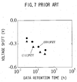
- Fig. 7 is a graph showing an amount of coercive voltage shift for the same ferroelectric capacitor.
- a ferroelectric capacitor that includes:
- a ferroelectric capacitor using a perovskite-type ferroelectric film belonging to a tetragonal system and oriented in the ⁇ 001> direction is provided with a perovskite-type ferroelectric layer belonging to a rhombohedral system along at least one interface with at least one of the upper and lower electrodes.
- PZT is a material having a composition that can be generally represented as Pb(Zr 1-x , Ti x )O 3 , where x is a composition parameter and a solid-solution is formed between PbZrO 3 end member and PbTiO 3 end member.
- x is a composition parameter
- a solid-solution is formed between PbZrO 3 end member and PbTiO 3 end member.
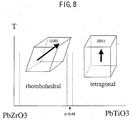
- Fig. 8 is a simplified phase-equilibrium diagram of PZT.
- the vertical axis represents temperature and the horizontal axis represents a composition parameter x.
- a phase belonging to the tetragonal system appears on the side where Ti is rich and a phase belonging to the rhombohedral system appears on the side where Zr is rich.
- a phase belonging to the orthorhombic system appears.
- phase belonging to the tetragonal system and the phase belonging to the rhombohedral system are both ferroelectric phases having spontaneous polarizations shown by arrows in Fig. 8.
- the PbZrO 3 phase belonging to the orthorhombic system does not show a ferroelectric property.
- the inventors have created a ferroelectric capacitor having a capacitor insulation film that is formed using not only the PZT film belonging to the tetragonal system but also a PZT film belonging to the rhombohedral system and have examined an imprint property of such a ferroelectric capacitor.
- Fig. 9 is a graph similar to that of Fig. 9 and shows a result of examination of imprint property for a ferroelectric capacitor in which PZT film of various crystal phases are used as a capacitor insulation film 16. The results shown in Fig. 7 are superimposed on a graph of Fig. 9.
- Fig. 1 is a cross-sectional diagram showing a FeRAM of the related art.
- Fig. 2 is a schematic diagram showing a structure of a ferroelectric capacitor of the related art.
- Fig. 3 is a graph showing electric characteristic of a ferroelectric capacitor of the related art.
- Fig. 4 is a diagram for explaining a fatigue produced in the ferroelectric capacitor.
- Fig. 5 is a diagram explaining an imprint deficiency produced in the ferroelectric capacitor.
- Fig. 6 is a graph showing an electric property of the ferroelectric capacitor of the related art.
- Fig. 7 is a diagram used for explaining a drawback of the ferroelectric capacitor of the related art.
- Fig. 8 is a simplified phase equilibrium diagram of the PZT system material.
- Fig. 9 is a diagram for explaining a principle of the present invention.
- Fig. 10 is a schematic diagram showing a structure of a ferroelectric capacitor of a first embodiment of the present invention.
- Figs. 11A through 11 D are diagrams showing various steps of a fabrication process of ferroelectric capacitors of a second and a third embodiment of the present invention.
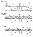
- Figs. 12A through 12C are diagrams showing various steps of fabricating FeRAM according to the fourth embodiment of the present invention.
- Fig.13D through 13F are diagrams showing further various steps of fabricating FeRAM according to the fourth embodiment of the present invention.
- Fig. 14G through 14I are diagrams showing further various steps of fabricating FeRAM according to the fourth embodiment of the present invention.
- Fig. 15J through 15L are diagrams showing further various steps of fabricating FeRAM according to the fourth embodiment of the present invention.
- Fig. 16M through 160 are diagrams showing further various steps of fabricating FeRAM according to the fourth embodiment of the present invention.
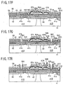
- Fig. 17P through 17R are diagrams showing further various steps of fabricating FeRAM according to the fourth embodiment of the present invention.
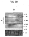
- FIG. 10 shows a ferroelectric capacitor 30 of a first embodiment of the present invention.
- a ferroelectric capacitor 30 is formed on a Si substrate 31 via a SiO 2 film 32.
- the ferroelectric capacitor 30 includes a lower electrode 33, a PZT film 34 formed on the lower electrode 33 and an upper electrode 35 formed on the PZT film 34.
- the lower film 33 is a Pt film that is mainly oriented in the ⁇ 100> direction and has a thickness of typically about 100 nm.
- the PZT film 34 includes a PZT film part 34A formed at an interface with the lower electrode 33, a PZT film part 34B provided on the PZT film part 34A and a PZT film part 34C provided on the PZT film part 34B at an interface with the upper electrode 35.
- the PZT film part 34A has a thickness of about 20 nm and is formed of PZT crystals belonging to the rhombohedral system.
- the PZT film part 34B has a thickness of about 180 nm and is formed of PZT crystals belongs to the tetragonal system.
- the PZT film part 34C has a thickness of about 20 nm and is formed of PZT crystals belonging to the tetragonal system.
- the PZT film part 34A has a composition Pb 1.05 (Zr 0.70 Ti 0.30 )O 3 . and is mainly oriented in the ⁇ 100> direction in accordance with the direction of orientation of the lower electrode 33.
- the PZT film part 34B formed on the PZT film part 34A has a composition Pb 1.05 (Zr 0.70 Ti 0.30 )O 3 and is mainly oriented in the ⁇ 100> direction.
- the PZT film part 34C formed on the PZT film part 34B is mainly oriented in the ⁇ 100> direction as in the case of the PZT film part 34A and has a composition Pb 1.05 (Zr 0.70 Ti 0.30 )O 3 .
- the ferroelectric capacitor 30 having such a structure, a major part of the PZT film 34 is the PZT film part 34B belonging to the tetragonal system oriented in the ⁇ 001> direction. Therefore, the ferroelectric capacitor 30 has a large remanent polarization and an improved retention property. Also, with such a ferroelectric capacitor, the PZT film parts 34A and 34C belonging to the rhombohedral system is provided at the interfaces with the upper and lower electrodes 33 and 35. Accordingly, it is understood that the shift of the coercive voltage caused by an accumulation of electric charges at the interfaces with the electrodes is reduced.
- PZT film parts 34A and 34C are not limited to the phase of the rhombohedral system but may also belong to the orthorhombic system shown in the phase equilibrium diagram of Fig. 8.
- the PZT film parts 34A and 34C belonging to the rhombohedral system need not be formed on both interfaces with the electrodes but the same effect may be obtained with either one of the PZT film parts.
- any one of the PZT film parts 34A through 34C may be a PLZT film including La and its composition is expressed as (Pb, La) (Zr, Ti)O 3 . Further, the above-mentioned PZT film parts 34A through 34C may contain Sr or Ca.
- the PZT film parts 34A and 34C belonging to the rhombohedral system are obtained by setting the composition parameter x in Pb(Zr 1-x , Ti x )O 3 to a value less than about 0.48 and the PZT film part 34B can be obtained by setting the composition parameter x to a value greater than or equal to about 0.48.
- a process of fabricating the ferroelectric capacitor 30 of Fig. 10 will be described as a second embodiment of the present invention.
- the Si substrate 31 provided with the SiO 2 film 32 is subjected to a sputtering process in an Ar atmosphere such that a Pt film serving as the lower electrode 33 is deposited with a thickness of about 200 nm.
- O 2 may be introduced in the sputtering atmosphere by an amount that is about 20% of the sputtering atmosphere, such that the produced Pt film is an ordinary film oriented in the normal ⁇ 111> direction but may be a film oriented in the ⁇ 100> direction. See, for example, M. H. Kim, et al., J. Mater. Res. Soc. Vol. 14, No. 3 (1999), pp. 634-637.
- a sol-gel solution of 2 weight % with a Pb:Zr:Ti ratio of 105:70:30 is applied on the structure shown in Fig. 11A and dried. Then, the structure undergoes a rapid heating process for 60 seconds at 700°C in an oxygen atmosphere.
- the PZT film part 34A of PZT crystals belonging to the rhombohedral system oriented in the ⁇ 100> direction and having a composition expressed as Pb 1.05 (Zr 0.70 Ti 0.30 )O 3 is formed with a thickness of about 20 nm.
- a sol-gel solution of 15 weight % with a Pb:Zr:Ti ratio of 105:45:55 is applied on the structure shown in Fig. 11B and dried. Then, the structure undergoes a rapid heating process for 60 seconds at 700°C in an oxygen atmosphere.
- the PZT film part 34A the PZT film part 34B of PZT crystals belonging to the tetragonal system oriented in the ⁇ 001> direction and having a composition expressed as Pb 1.05 (Zr 0.45 Ti 0.55 )O 3 is formed with a thickness of about 180 nm.
- the PZT film part 34C of rhombohedral system is formed with a step similar to the step of fabricating the above-mentioned PZT film part 34A. Further, a Pt upper electrode 35 is formed on the PZT film part 34C by a normal sputtering process. Thus, the above-mentioned ferroelectric capacitor 30 is obtained.
- a ferroelectric capacitor having a PZT film oriented in the ⁇ 111> direction as the PZT film has been formed by a similar process. It is found that for the ferroelectric capacitor 30 formed in accordance with the present embodiment, a value of the remanent polarization Pr is increased by a factor of 1.5 of the comparative ferroelectric capacitor. This may be because the PZT film 34B in the capacitor insulation film 34 is oriented in the ⁇ 001> direction.
- the amount of shift of the coercive voltage Vc is less than 0.1 V for the ferroelectric capacitor 30 of the present embodiment that is substantially improved as compared to the comparative ferroelectric capacitor having 0.43 V shift of the coercive voltage.
- the electric property is improved as compared to the ferroelectric capacitor of the related art that used the PZT film oriented in the ⁇ 111> direction.
- the PZT film is formed on the Pt electrode oriented in the ⁇ 100> direction, but the PZT film may also be formed on an ordinary Pt electrode having an (111) orientation that is oriented in the ⁇ 111> direction.
- the PZT film may be formed by a sputtering process.
- an amorphous PZT film with a Ti composition x being less than 0.48 (x ⁇ 0.48) is crystallized by a rapid heating process in an oxygen atmosphere to form the PZT film 34A belonging to the rhombohedral system.
- an amorphous PZT film of a Ti composition x being greater than or equal to 0.48 (0.48 ⁇ x) is formed by a sputtering process.
- the amorphous PZT film is crystallized in an oxygen atmosphere to form a PZT film 34A belonging to the tetragonal system.
- the PZT film 34C belonging to the rhombohedral system is formed by sputtering and rapid heating processes.
- PZT films 34A, 34B and 34C may be formed by a CVD method.
- a method of fabricating a ferroelectric capacitor of a third embodiment of the present invention will be described, wherein the PZT films 34A, 34B and 34C are formed by a CVD process.
- the step of Fig. 11A is the same as the previous embodiment.
- a Pt film oriented in the ⁇ 100> direction is formed as the lower electrode 33 on the SiO 2 film 32 covering the Si substrate 31.
- a sample of the structure shown in Fig. 11A is introduced into a processing container of a CVD apparatus (not shown).
- An internal pressure of the processing container is set to a range between 130 and 1300 Pa and the temperature of the substrate under process is set to a range between 500 to 600 °C.
- Pb(DPM) 2 , Zr(DMHD) 4 and Ti(iPrO) 2 (DPM) 2 diluted with THF are introduced into the processing container as Pb, Zr and Ti vapor phase materials with a flow ratio of 1:0.56:0.46.
- a carrier gas containing for example Ar or He and an oxidation gas such as O 2 gas are also introduced into the processing container.
- the PZT film part 34A of the rhombohedral system is grown on the Pt film 33 with a thickness of about 20 nm.
- the flow ratio of the above-mentioned vapor phase material is altered to 1:0.55:0.55.
- the PZT film part 34B of the tetragonal system is grown the PZT film part 34A 33 with a thickness of about 180 nm.
- Pb(DPM) 2 Pb (C 11 H 19 O 2 ) 2
- Pb(C 5 H 7 O 2 ) 2 and Pb(C 11 H 19 O 2 )2(C 10 H 22 O 5 ) can be used as the vapor phase material of Pb.
- Zr(DMHD) 4 Zr(DPM) 4 and Zr(tBuO)(DPM) 3 can be used as the vapor phase material of Zr.
- Ti(iPrO) 2 (DPM) 2 described above Ti(i-PrO) 2 (DMHD) 2 and Ti(t-AmylO) 2 (DMHD) 2 can be used as the vapor phase material of Ti.
- a p-type well 41A and an n-type well 41B are formed on a p-type or an n-type Si substrate 41. Further, field oxide films 42 defining respective active regions are provided on the Si substrate 41 in the wells 41A and 41B.
- Gate oxide films 43 are formed on the active regions of the p-type well 41A and the n-type well 41B.
- a p-type polysilicon gate electrode 44A is formed on the gate oxide film 32 and for the n-type well 41B, an n-type polysilicon gate electrode 44B is formed on the gate oxide film 43.
- polysilicon interconnection patterns 44C and 44D extend on the field oxide films 42 in a manner similar to the polysilicon gate electrodes 44A and 44B.
- n-type impurities are ion implanted into the active region of the p-type well 41A using the gate electrode 44A and side wall insulation films on both sides of the gate electrode 44A as a self-aligning mask so as to form n-type diffusion regions 41a and 41b.
- p-type impurities are ion implanted into the active region of the n-type well 41B using the gate electrode 44B and side wall insulation films on both sides of the gate electrode 44B as a self-aligning mask so as to form p-type diffusion regions 41c and 41d.
- a SiON film 45 having a thickness of about 200 nm is deposited by performing a CVD process on the structure shown in Fig. 12B. Further, a SiO 2 film 46 having a thickness of about 1000 nm is deposited thereon.
- the SiO 2 film 46 is polished and planarized by a CMP (chemical mechanical polishing) process with the SiON film 45 being used as a stopper.
- contact holes 46A to 46D are formed through the planarized SiO 2 film 36 such that the diffusion regions 41a, 41b, 41c and 41d are exposed, respectively.
- the SiO 2 film 46 is further provided with a contact hole 46E that exposes the connection pattern 44C.
- a W layer 47 is deposited on the structure of Fig. 13D so as to fill the contact holes 46A to 46E. Further, in a step shown in Fig. 13F, the W layer 47 thus deposited is subjected to a CMP process with the SiO 2 film 46 being used as a stopper. As a result of the polishing process, there are formed W plugs 47A to 47E in correspondence to the contact holes 46A to 46E, respectively.
- an oxidization stopper film 48 of SiON and an SiO 2 film 49 are deposited consecutively on the structure of Fig. 13F respectively with the thicknesses of 100 nm and 130 nm, respectively, followed by a heating process at 650°C for 30 minutes conducted in an N 2 atmosphere such that a sufficient degassing process is performed.
- a Ti film 50 and a Pt film 51 are deposited consecutively on the SiO 2 film 49 with respective thicknesses of 20 nm and 175 nm by a sputtering process.
- the Ti film 50 and the Pt film 51 thereon constitute a lower electrode layer. It is preferable that the sputtering process of the Pt film 51 is conducted in an Ar gas with 20% O 2 gas being added thereto.
- the PZT or PLZT film 52 are deposited with a thickness of about 220 nm in the CVD apparatus.
- deposition of the PZT or PLZT film 52 is performed by firstly depositing a PZT or PLZT film belonging to the rhombohedral system with a Ti composition x being less than 0.48 (x ⁇ 0.48) with a thickness of about 20 nm, then depositing a PZT or PLZT film belonging to the tetragonal system with a Ti composition x being greater than or equal to 0.48 (0.48 ⁇ x) with a thickness of about 180 nm and further depositing a PZT or PLZT film belonging to the rhombohedral system with a Ti composition x being less than 0.48 (x ⁇ 0.48) with a thickness of about 20 nm.
- the substrate 41 is returned to the sputtering apparatus after the above-mentioned rapid thermal processing step.
- a Pt film, an IrO 2 film or an SrRuO 3 film is deposited on the ferroelectric film 52 with a thickness of about 200 nm to form the upper electrode layer 53.
- a resist pattern is formed on the upper electrode layer 53 and the upper electrode layer 53 is dry-etched using the resist pattern as a mask, such that an upper electrode pattern 53A is formed on the ferroelectric film 52 in correspondence with the upper electrode layer 53.
- an annealing process is conducted in an O 2 atmosphere for 60 minutes at 650 °C so as to remove any damage caused in the ferroelectric film 52 during a sputtering or patterning process of the upper electrode layer 53.
- a resist pattern corresponding to a capacitor insulating layer pattern of the desired ferroelectric capacitor is formed on the ferroelectric film 52.
- the ferroelectric film 52 is dry-etched using the resist pattern as a mask to form a capacitor insulation film pattern 52A.
- a sputtering process is conducted under the same condition as for the ferroelectric capacitor layer 52 such that an encapping layer 52 of the same material as the ferroelectic capacitor layer 52 is deposited that has a thickness of about 20 nm, and in the O 2 atmosphere, a rapid heating process is performed for 60 seconds at 700°C.
- the encapping layer 52B protects the ferroelectric film 52A from reduction.
- a resist pattern corresponding to the desired lower electrode pattern is formed on the lower electrode layer 51, or, the encapping layer 52B, and the encapping layer 52B and underlying lower electrode layers 50, 51 are dry-etched using the resist pattern as a mask to form a lower electrode 51A.
- the resist pattern is removed and a heating process is conducted in the O 2 atmosphere for 60 minutes at 650°C so as to remove damages caused in the ferroelectric film 52A during the dry-etching process.
- an SiO 2 film 54 is deposited on the structure shown in Fig. 15K by the CVD process with a thickness of typically about 200 nm. Further, an SOG film 55 is deposited thereon to reduce the level difference at stepped parts. The SiO 2 film 54 and the SOG film 55 form an interlayer insulation film 56.
- a contact hole 56A that exposes the upper electrode pattern 53A and a contact hole 56B that exposes the lower electrode pattern 51A are formed in the interlayer insulation film 56.
- contact holes 56C and 56D that expose the W plugs 47B and 47D, respectively, are formed through the interlayer insulation film 56 and the underlying SiO 2 film 49 and SiON anti-oxidation film 48.
- a heating process is conducted in an O 2 atmosphere for 60 minutes at 550 °C, so as to remove any damage caused during the dry-etching process.
- a local interconnection pattern 57A that electrically connects the contact hole 56A and the contact hole 56C is formed by a TiN film and a similar local interconnection patterns 57B and 57C are also formed on the contact holes 56B and 56D.
- an SiO 2 film 58 is formed on the structure shown in Fig. 160.
- contact holes 58A, 58B and 58C that expose the W plug 47A, the local interconnection pattern 57B and the W plug 47C, respectively, are formed in the SiO 2 film 58.
- electrodes 59A, 59B and 59C are formed in correspondence with the contact holes 58A, 58B and 58C.
- the steps of forming an interlayer insulation film and a local interconnection pattern may be repeated to form a multi-level metallization structure.
Landscapes
- Semiconductor Memories (AREA)
- Semiconductor Integrated Circuits (AREA)
Abstract
Description
Claims (14)
- A ferroelectric capacitor (30) comprising:characterized in that said ferroelectric film (34) includes a first ferroelectric film part (34A, 34C) having a first crystal system and formed along at least one interface with at least one of said lower electrode (33) and said upper electrode (35) and a second ferroelectric film part (34B) having a second crystal system that is different from said first crystal system.a lower electrode (33);a ferroelectric film (34) provided over said lower electrode (33) and having a perovskite-type structure; andan upper electrode (35) provided over said ferroelectric film (34),
- The ferroelectric capacitor (30) as claimed in claim 1, characterized in that said first crystal system is a rhombohedral system and said second crystal system is a tetragonal system.
- The ferroelectric capacitor (30) as claimed in claim 1, characterized in that said first ferroelectric film part (34A, 34C) forms a first layer and a second layer that are formed along said lower electrode (33) and said upper electrode (35), respectively, and said second ferroelectric film part (34B) is formed between said first layer and said second layer.
- The ferroelectric capacitor (30) as claimed in claim 1, characterized in that said first and second ferroelectric film parts (34A, 34B ,34C) each contains Pb, Zr and Ti.
- The ferroelectric capacitor (30) as claimed in claim 1, characterized in that said first and second ferroelectric film parts (34A, 34B ,34C) have a composition expressed as Pb(Zr1-x, Tix)O3, where x represents a composition parameter that is less than 0.48 (x<0.48) for said first ferroelectric film part (34A, 34C) and greater than or equal to 0.48 (0.48 ≦ x) for said second ferroelectric film part (34B).
- The ferroelectric capacitor (30) as claimed in claim 1, characterized in that said second ferroelectric film part (34B) is oriented in the <001> direction.
- The ferroelectric capacitor (30) as claimed in claim 1, characterized in that said second ferroelectric film part (34B) is oriented in the <111> direction.
- The ferroelectric capacitor (30) as claimed in claim 1, characterized in that said lower electrode (33) is oriented in the <100> direction.
- The ferroelectric capacitor (30) as claimed in claim 1, characterized in that said lower electrode (33) is oriented in the <111> direction.
- The ferroelectric capacitor (30) as claimed in claim 1, characterized in that said first crystal system is an orthorhombic system and said second crystal system is a tetragonal system.
- The ferroelectric capacitor (30) as claimed in claim 1, characterized in that said first and second ferroelectric film parts (34A, 34B, 34C) are formed by a CVD process.
- The ferroelectric capacitor (30) as claimed in claim 1, characterized in that said first and second ferroelectric film parts (34A, 34B, 34C) are formed by a sol-gel process.
- The ferroelectric capacitor (30) as claimed in claim 1, characterized in that said first and second ferroelectric film parts (34A, 34B, 34C) are formed by a sputtering process.
- A semiconductor device comprising:characterized in that said ferroelectric capacitor (30) comprises:a substrate (31);a transistor formed on said substrate;an interlayer insulation film formed on said substrate to cover said transistor; anda ferroelectric capacitor (30) formed on said interlayer insulation film,a lower electrode (33);a ferroelectric film (34) provided over said lower electrode (33) and having a perovskite-type structure; andan upper electrode (35) provided over said ferroelectric film (34),said ferroelectric film (34) including a first ferroelectric film part (34A, 34C) having a first crystal system and formed along at least one interface with at least one of said lower electrode (33) and said upper electrode (35) and a second ferroelectric film part (34B) having a second crystal system that is different from said first crystal system.
Applications Claiming Priority (2)
| Application Number | Priority Date | Filing Date | Title |
|---|---|---|---|
| JP2001336576 | 2001-11-01 | ||
| JP2001336576A JP3971598B2 (en) | 2001-11-01 | 2001-11-01 | Ferroelectric capacitor and semiconductor device |
Publications (3)
| Publication Number | Publication Date |
|---|---|
| EP1308990A2 true EP1308990A2 (en) | 2003-05-07 |
| EP1308990A3 EP1308990A3 (en) | 2007-09-26 |
| EP1308990B1 EP1308990B1 (en) | 2014-07-16 |
Family
ID=19151377
Family Applications (1)
| Application Number | Title | Priority Date | Filing Date |
|---|---|---|---|
| EP02007739.2A Expired - Lifetime EP1308990B1 (en) | 2001-11-01 | 2002-04-05 | Ferroelectric capacitor and a semiconductor device |
Country Status (6)
| Country | Link |
|---|---|
| US (2) | US6841817B2 (en) |
| EP (1) | EP1308990B1 (en) |
| JP (1) | JP3971598B2 (en) |
| KR (1) | KR100711742B1 (en) |
| CN (1) | CN1204625C (en) |
| TW (1) | TW522555B (en) |
Cited By (1)
| Publication number | Priority date | Publication date | Assignee | Title |
|---|---|---|---|---|
| US7229662B2 (en) | 2003-12-16 | 2007-06-12 | National University Of Singapore | Heterolayered ferroelectric thin films and methods of forming same |
Families Citing this family (31)
| Publication number | Priority date | Publication date | Assignee | Title |
|---|---|---|---|---|
| US20050094457A1 (en) * | 1999-06-10 | 2005-05-05 | Symetrix Corporation | Ferroelectric memory and method of operating same |
| JP3971598B2 (en) * | 2001-11-01 | 2007-09-05 | 富士通株式会社 | Ferroelectric capacitor and semiconductor device |
| KR100611707B1 (en) | 2002-05-28 | 2006-08-11 | 가부시끼가이샤 도시바 | Semiconductor device and manufacturing method thereof |
| JP4040397B2 (en) * | 2002-08-29 | 2008-01-30 | 富士通株式会社 | Device having capacitive element and method of manufacturing the same |
| JP4315676B2 (en) * | 2002-12-26 | 2009-08-19 | Necエレクトロニクス株式会社 | Semiconductor memory device and manufacturing method thereof |
| KR20040070564A (en) * | 2003-02-04 | 2004-08-11 | 삼성전자주식회사 | Ferroelectric capacitor and method of manufacturing the same |
| US20050145908A1 (en) * | 2003-12-30 | 2005-07-07 | Moise Theodore S.Iv | High polarization ferroelectric capacitors for integrated circuits |
| WO2005074032A1 (en) * | 2004-01-28 | 2005-08-11 | Fujitsu Limited | Semiconductor device and its manufacturing method |
| US20050161717A1 (en) * | 2004-01-28 | 2005-07-28 | Fujitsu Limited | Semiconductor device and method of fabricating the same |
| JP4616830B2 (en) * | 2004-04-28 | 2011-01-19 | 富士通株式会社 | Manufacturing method of semiconductor device |
| US7528530B2 (en) * | 2005-08-23 | 2009-05-05 | Canon Kabushiki Kaisha | Piezoelectric substance, piezoelectric substance element, liquid discharge head, liquid discharge device and method for producing piezoelectric substance |
| US7998362B2 (en) * | 2005-08-23 | 2011-08-16 | Canon Kabushiki Kaisha | Piezoelectric substance, piezoelectric element, liquid discharge head using piezoelectric element, liquid discharge apparatus, and production method of piezoelectric element |
| JP2007088147A (en) * | 2005-09-21 | 2007-04-05 | Toshiba Corp | Semiconductor device and manufacturing method thereof |
| US7692310B2 (en) * | 2006-03-27 | 2010-04-06 | Intel Corporation | Forming a hybrid device |
| JP2007266429A (en) * | 2006-03-29 | 2007-10-11 | Fujitsu Ltd | Semiconductor device and manufacturing method thereof |
| JP5007528B2 (en) * | 2006-06-12 | 2012-08-22 | セイコーエプソン株式会社 | Method for manufacturing piezoelectric element |
| JP5326256B2 (en) * | 2007-10-23 | 2013-10-30 | 富士通セミコンダクター株式会社 | Manufacturing method of semiconductor device |
| US8471049B2 (en) * | 2008-12-10 | 2013-06-25 | Air Product And Chemicals, Inc. | Precursors for depositing group 4 metal-containing films |
| JP2010258046A (en) * | 2009-04-21 | 2010-11-11 | Ulvac Japan Ltd | Method for forming pzt thin film, and method for manufacturing semiconductor device |
| US8389300B2 (en) * | 2010-04-02 | 2013-03-05 | Centre National De La Recherche Scientifique | Controlling ferroelectricity in dielectric films by process induced uniaxial strain |
| JP5360023B2 (en) * | 2010-09-06 | 2013-12-04 | 富士通株式会社 | Semiconductor device and manufacturing method thereof |
| JP5655585B2 (en) * | 2011-01-20 | 2015-01-21 | 富士通セミコンダクター株式会社 | Manufacturing method of semiconductor device |
| US9761785B2 (en) | 2011-10-17 | 2017-09-12 | The United States Of America As Represented By The Secretary Of The Army | Stylo-epitaxial piezoelectric and ferroelectric devices and method of manufacturing |
| US8866367B2 (en) | 2011-10-17 | 2014-10-21 | The United States Of America As Represented By The Secretary Of The Army | Thermally oxidized seed layers for the production of {001} textured electrodes and PZT devices and method of making |
| US20130093290A1 (en) * | 2011-10-17 | 2013-04-18 | U.S. Government As Represented By The Secretary Of The Army | Stylo-Epitaxial Piezoelectric and Ferroelectric Devices and Method of Manufacturing |
| US10266936B2 (en) | 2011-10-17 | 2019-04-23 | The United States Of America As Represented By The Secretary Of The Army | Process for making lead zirconate titanate (PZT) layers and/or platinum electrodes and products thereof |
| JP6141080B2 (en) * | 2012-04-19 | 2017-06-07 | 新科實業有限公司SAE Magnetics(H.K.)Ltd. | Thin film piezoelectric element and manufacturing method thereof, microactuator, head gimbal assembly, and disk drive device including the same |
| DE102012105036A1 (en) * | 2012-06-12 | 2013-12-12 | Pyreos Ltd. | Method of manufacturing a microsystem |
| WO2019005174A1 (en) * | 2017-06-30 | 2019-01-03 | Intel Corporation | Apparatus for generating rf second and higher harmonics |
| KR102813679B1 (en) * | 2021-01-22 | 2025-05-27 | 삼성전자주식회사 | Semiconductor device and method for fabricating the same |
| US11690228B2 (en) * | 2021-02-25 | 2023-06-27 | Taiwan Semiconductor Manufacturing Company, Ltd. | Annealed seed layer to improve ferroelectric properties of memory layer |
Family Cites Families (42)
| Publication number | Priority date | Publication date | Assignee | Title |
|---|---|---|---|---|
| JP2583882B2 (en) | 1987-03-26 | 1997-02-19 | 松下電器産業株式会社 | Oriented perovskite-type compound laminated film |
| JP2544836B2 (en) | 1990-11-06 | 1996-10-16 | 三菱電機株式会社 | Capacitor |
| US5850089A (en) * | 1992-03-13 | 1998-12-15 | American Research Corporation Of Virginia | Modulated-structure of PZT/PT ferroelectric thin films for non-volatile random access memories |
| US5572052A (en) * | 1992-07-24 | 1996-11-05 | Mitsubishi Denki Kabushiki Kaisha | Electronic device using zirconate titanate and barium titanate ferroelectrics in insulating layer |
| JPH0689986A (en) | 1992-07-24 | 1994-03-29 | Mitsubishi Electric Corp | Electronic device and its manufacturing method |
| US5387459A (en) * | 1992-12-17 | 1995-02-07 | Eastman Kodak Company | Multilayer structure having an epitaxial metal electrode |
| US5650362A (en) * | 1993-11-04 | 1997-07-22 | Fuji Xerox Co. | Oriented conductive film and process for preparing the same |
| JP3476932B2 (en) * | 1994-12-06 | 2003-12-10 | シャープ株式会社 | Ferroelectric thin film, substrate coated with ferroelectric thin film, and method of manufacturing ferroelectric thin film |
| JP3890634B2 (en) * | 1995-09-19 | 2007-03-07 | セイコーエプソン株式会社 | Piezoelectric thin film element and ink jet recording head |
| US5683614A (en) * | 1996-08-16 | 1997-11-04 | Sandia Corporation | Sol-gel type synthesis of Bi2 (Sr,Ta2)O9 using an acetate based system |
| US5719417A (en) * | 1996-11-27 | 1998-02-17 | Advanced Technology Materials, Inc. | Ferroelectric integrated circuit structure |
| JPH10214945A (en) | 1997-01-30 | 1998-08-11 | Sharp Corp | Ferroelectric thin film coated substrate, capacitor structure element, and method of manufacturing ferroelectric thin film coated substrate |
| US6080499A (en) * | 1997-07-18 | 2000-06-27 | Ramtron International Corporation | Multi-layer approach for optimizing ferroelectric film performance |
| KR100275726B1 (en) * | 1997-12-31 | 2000-12-15 | 윤종용 | Ferroelectric memory device and fabrication method thereof |
| JP3520403B2 (en) * | 1998-01-23 | 2004-04-19 | セイコーエプソン株式会社 | Piezoelectric thin film element, actuator, ink jet recording head, and ink jet recording apparatus |
| JP3594787B2 (en) * | 1998-02-03 | 2004-12-02 | 富士通株式会社 | Semiconductor device and manufacturing method thereof |
| JP4122564B2 (en) * | 1998-04-24 | 2008-07-23 | セイコーエプソン株式会社 | Piezoelectric element, ink jet recording head and manufacturing method thereof |
| US6258459B1 (en) * | 1998-04-28 | 2001-07-10 | Tdk Corporation | Multilayer thin film |
| US5900274A (en) * | 1998-05-01 | 1999-05-04 | Eastman Kodak Company | Controlled composition and crystallographic changes in forming functionally gradient piezoelectric transducers |
| JPH11330411A (en) * | 1998-05-13 | 1999-11-30 | Matsushita Electric Ind Co Ltd | Semiconductor memory device and method of manufacturing the same |
| US6541375B1 (en) * | 1998-06-30 | 2003-04-01 | Matsushita Electric Industrial Co., Ltd. | DC sputtering process for making smooth electrodes and thin film ferroelectric capacitors having improved memory retention |
| JP3482883B2 (en) * | 1998-08-24 | 2004-01-06 | 株式会社村田製作所 | Ferroelectric thin film element and method of manufacturing the same |
| DE19842816C1 (en) * | 1998-09-18 | 2000-02-03 | Siemens Ag | Self-polarised ferroelectric layer manufacture |
| US6376090B1 (en) * | 1998-09-25 | 2002-04-23 | Sharp Kabushiki Kaisha | Method for manufacturing a substrate with an oxide ferroelectric thin film formed thereon and a substrate with an oxide ferroelectric thin film formed thereon |
| US20020153543A1 (en) * | 1998-09-29 | 2002-10-24 | Takeshi Kijima | Method for manufacturing oxide ferroelectric thin film oxide ferroelectric thin film and oxide ferroelectric thin film element |
| AU1539900A (en) * | 1998-11-30 | 2000-06-19 | Interuniversitair Micro-Elektronica Centrum | Method of fabrication of a ferro-electric capacitor and method of growing a pzt layer on a substrate |
| US6385355B1 (en) * | 1999-03-15 | 2002-05-07 | Fuji Xerox Co., Ltd. | Optical deflection element |
| JP2000286396A (en) * | 1999-03-31 | 2000-10-13 | Yamaha Corp | Ferroelectric memory and manufacture thereof |
| JP2000031399A (en) | 1999-06-09 | 2000-01-28 | Seiko Epson Corp | Dielectric element and semiconductor storage device |
| US6495878B1 (en) * | 1999-08-02 | 2002-12-17 | Symetrix Corporation | Interlayer oxide containing thin films for high dielectric constant application |
| JP2001196652A (en) | 1999-11-01 | 2001-07-19 | Kansai Research Institute | Piezoelectric element, manufacturing method thereof and ink jet printer head using the same |
| US6523943B1 (en) * | 1999-11-01 | 2003-02-25 | Kansai Research Institute, Inc. | Piezoelectric element, process for producing the piezoelectric element, and head for ink-jet printer using the piezoelectric element |
| JP3401558B2 (en) * | 1999-12-14 | 2003-04-28 | 独立行政法人産業技術総合研究所 | Epitaxial composite structure and element using the same |
| US6277254B1 (en) * | 1999-12-16 | 2001-08-21 | Honeywell International Inc. | Ceramic compositions, physical vapor deposition targets and methods of forming ceramic compositions |
| US6576546B2 (en) * | 1999-12-22 | 2003-06-10 | Texas Instruments Incorporated | Method of enhancing adhesion of a conductive barrier layer to an underlying conductive plug and contact for ferroelectric applications |
| US6526833B1 (en) * | 2000-03-13 | 2003-03-04 | Massachusetts Institute Of Technology | Rhombohedral-phase barium titanate as a piezoelectric transducer |
| US6627930B1 (en) * | 2000-03-14 | 2003-09-30 | Fujitsu Limited | Ferroelectric thin film capacitors having multi-layered crystallographic textures |
| US6709776B2 (en) * | 2000-04-27 | 2004-03-23 | Tdk Corporation | Multilayer thin film and its fabrication process as well as electron device |
| JP2002170938A (en) * | 2000-04-28 | 2002-06-14 | Sharp Corp | Semiconductor device and method of manufacturing the same |
| JP4257485B2 (en) * | 2000-06-21 | 2009-04-22 | セイコーエプソン株式会社 | Ceramic film, manufacturing method thereof, semiconductor device, and piezoelectric element |
| US6507060B2 (en) * | 2001-05-23 | 2003-01-14 | Winbond Electronics Corp. | Silicon-based PT/PZT/PT sandwich structure and method for manufacturing the same |
| JP3971598B2 (en) * | 2001-11-01 | 2007-09-05 | 富士通株式会社 | Ferroelectric capacitor and semiconductor device |
-
2001
- 2001-11-01 JP JP2001336576A patent/JP3971598B2/en not_active Expired - Fee Related
-
2002
- 2002-03-25 US US10/103,894 patent/US6841817B2/en not_active Expired - Lifetime
- 2002-03-26 TW TW091105936A patent/TW522555B/en not_active IP Right Cessation
- 2002-04-05 EP EP02007739.2A patent/EP1308990B1/en not_active Expired - Lifetime
- 2002-04-12 KR KR1020020020105A patent/KR100711742B1/en not_active Expired - Fee Related
- 2002-04-19 CN CNB021161178A patent/CN1204625C/en not_active Expired - Fee Related
-
2004
- 2004-10-19 US US10/967,210 patent/US7423308B2/en not_active Expired - Fee Related
Cited By (1)
| Publication number | Priority date | Publication date | Assignee | Title |
|---|---|---|---|---|
| US7229662B2 (en) | 2003-12-16 | 2007-06-12 | National University Of Singapore | Heterolayered ferroelectric thin films and methods of forming same |
Also Published As
| Publication number | Publication date |
|---|---|
| CN1416173A (en) | 2003-05-07 |
| US20050052823A1 (en) | 2005-03-10 |
| JP2003142657A (en) | 2003-05-16 |
| US20030080329A1 (en) | 2003-05-01 |
| EP1308990A3 (en) | 2007-09-26 |
| CN1204625C (en) | 2005-06-01 |
| US7423308B2 (en) | 2008-09-09 |
| JP3971598B2 (en) | 2007-09-05 |
| TW522555B (en) | 2003-03-01 |
| US6841817B2 (en) | 2005-01-11 |
| KR20030038307A (en) | 2003-05-16 |
| KR100711742B1 (en) | 2007-04-25 |
| EP1308990B1 (en) | 2014-07-16 |
Similar Documents
| Publication | Publication Date | Title |
|---|---|---|
| EP1308990B1 (en) | Ferroelectric capacitor and a semiconductor device | |
| US7745232B2 (en) | Semiconductor device and method of manufacturing the same | |
| US6645779B2 (en) | FeRAM (ferroelectric random access memory) and method for forming the same | |
| US20080199975A1 (en) | Methods of forming a metal oxide layer pattern having a decreased line width of a portion thereof and methods of manufacturing a semiconductor device using the same | |
| KR19980064695A (en) | Capacitor Structure of Semiconductor Memory Cell and Manufacturing Method Thereof | |
| US8349679B2 (en) | Semiconductor device and method of manufacturing the same | |
| US6608339B2 (en) | Ferroelectric memory element | |
| US6495412B1 (en) | Semiconductor device having a ferroelectric capacitor and a fabrication process thereof | |
| US6777287B2 (en) | Ferroelectric semiconductor memory device and a fabrication process thereof | |
| US6747302B2 (en) | FeRAM having BLT ferroelectric layer and method for forming the same | |
| US20030235969A1 (en) | Semiconductor device manufacturing method | |
| US7015531B2 (en) | FeRAM having bottom electrode connected to storage node and method for forming the same | |
| JPH06275840A (en) | Nonvolatile storage element | |
| JP4801078B2 (en) | Manufacturing method of semiconductor device | |
| JPH10270651A (en) | Semiconductor storage device | |
| JP2002043310A (en) | Method of forming ferroelectric film and method of manufacturing semiconductor device | |
| KR100801202B1 (en) | Manufacturing Method of Semiconductor Device |
Legal Events
| Date | Code | Title | Description |
|---|---|---|---|
| PUAI | Public reference made under article 153(3) epc to a published international application that has entered the european phase |
Free format text: ORIGINAL CODE: 0009012 |
|
| AK | Designated contracting states |
Designated state(s): AT BE CH CY DE DK ES FI FR GB GR IE IT LI LU MC NL PT SE TR |
|
| AX | Request for extension of the european patent |
Extension state: AL LT LV MK RO SI |
|
| PUAL | Search report despatched |
Free format text: ORIGINAL CODE: 0009013 |
|
| AK | Designated contracting states |
Kind code of ref document: A3 Designated state(s): AT BE CH CY DE DK ES FI FR GB GR IE IT LI LU MC NL PT SE TR |
|
| AX | Request for extension of the european patent |
Extension state: AL LT LV MK RO SI |
|
| 17P | Request for examination filed |
Effective date: 20071009 |
|
| 17Q | First examination report despatched |
Effective date: 20071113 |
|
| AKX | Designation fees paid |
Designated state(s): FR IT |
|
| REG | Reference to a national code |
Ref country code: DE Ref legal event code: 8566 |
|
| RAP1 | Party data changed (applicant data changed or rights of an application transferred) |
Owner name: FUJITSU MICROELECTRONICS LIMITED |
|
| RAP1 | Party data changed (applicant data changed or rights of an application transferred) |
Owner name: FUJITSU SEMICONDUCTOR LIMITED |
|
| REG | Reference to a national code |
Ref country code: DE Ref legal event code: R079 Free format text: PREVIOUS MAIN CLASS: H01L0021020000 Ipc: H01L0049020000 |
|
| GRAP | Despatch of communication of intention to grant a patent |
Free format text: ORIGINAL CODE: EPIDOSNIGR1 |
|
| RIC1 | Information provided on ipc code assigned before grant |
Ipc: H01L 49/02 20060101AFI20140305BHEP Ipc: H01L 27/115 20060101ALI20140305BHEP |
|
| INTG | Intention to grant announced |
Effective date: 20140321 |
|
| GRAS | Grant fee paid |
Free format text: ORIGINAL CODE: EPIDOSNIGR3 |
|
| GRAA | (expected) grant |
Free format text: ORIGINAL CODE: 0009210 |
|
| AK | Designated contracting states |
Kind code of ref document: B1 Designated state(s): FR IT |
|
| PLBE | No opposition filed within time limit |
Free format text: ORIGINAL CODE: 0009261 |
|
| STAA | Information on the status of an ep patent application or granted ep patent |
Free format text: STATUS: NO OPPOSITION FILED WITHIN TIME LIMIT |
|
| 26N | No opposition filed |
Effective date: 20150417 |
|
| REG | Reference to a national code |
Ref country code: FR Ref legal event code: PLFP Year of fee payment: 15 |
|
| REG | Reference to a national code |
Ref country code: FR Ref legal event code: PLFP Year of fee payment: 16 |
|
| PGFP | Annual fee paid to national office [announced via postgrant information from national office to epo] |
Ref country code: FR Payment date: 20170313 Year of fee payment: 16 |
|
| REG | Reference to a national code |
Ref country code: FR Ref legal event code: CA Effective date: 20170726 |
|
| PGFP | Annual fee paid to national office [announced via postgrant information from national office to epo] |
Ref country code: IT Payment date: 20170420 Year of fee payment: 16 |
|
| PG25 | Lapsed in a contracting state [announced via postgrant information from national office to epo] |
Ref country code: FR Free format text: LAPSE BECAUSE OF NON-PAYMENT OF DUE FEES Effective date: 20180430 Ref country code: IT Free format text: LAPSE BECAUSE OF NON-PAYMENT OF DUE FEES Effective date: 20180405 |