EP1308958A2 - Three dimensional large storage random access memory device - Google Patents
Three dimensional large storage random access memory device Download PDFInfo
- Publication number
- EP1308958A2 EP1308958A2 EP02257425A EP02257425A EP1308958A2 EP 1308958 A2 EP1308958 A2 EP 1308958A2 EP 02257425 A EP02257425 A EP 02257425A EP 02257425 A EP02257425 A EP 02257425A EP 1308958 A2 EP1308958 A2 EP 1308958A2
- Authority
- EP
- European Patent Office
- Prior art keywords
- memory
- plane
- array
- electrically connected
- select
- Prior art date
- Legal status (The legal status is an assumption and is not a legal conclusion. Google has not performed a legal analysis and makes no representation as to the accuracy of the status listed.)
- Granted
Links
Images



Classifications
-
- H—ELECTRICITY
- H10—SEMICONDUCTOR DEVICES; ELECTRIC SOLID-STATE DEVICES NOT OTHERWISE PROVIDED FOR
- H10B—ELECTRONIC MEMORY DEVICES
- H10B12/00—Dynamic random access memory [DRAM] devices
- H10B12/50—Peripheral circuit region structures
-
- G—PHYSICS
- G11—INFORMATION STORAGE
- G11C—STATIC STORES
- G11C5/00—Details of stores covered by group G11C11/00
- G11C5/06—Arrangements for interconnecting storage elements electrically, e.g. by wiring
-
- G—PHYSICS
- G11—INFORMATION STORAGE
- G11C—STATIC STORES
- G11C13/00—Digital stores characterised by the use of storage elements not covered by groups G11C11/00, G11C23/00, or G11C25/00
- G11C13/0002—Digital stores characterised by the use of storage elements not covered by groups G11C11/00, G11C23/00, or G11C25/00 using resistive RAM [RRAM] elements
- G11C13/0021—Auxiliary circuits
- G11C13/0023—Address circuits or decoders
-
- G—PHYSICS
- G11—INFORMATION STORAGE
- G11C—STATIC STORES
- G11C5/00—Details of stores covered by group G11C11/00
- G11C5/02—Disposition of storage elements, e.g. in the form of a matrix array
-
- G—PHYSICS
- G11—INFORMATION STORAGE
- G11C—STATIC STORES
- G11C5/00—Details of stores covered by group G11C11/00
- G11C5/02—Disposition of storage elements, e.g. in the form of a matrix array
- G11C5/025—Geometric lay-out considerations of storage- and peripheral-blocks in a semiconductor storage device
-
- G—PHYSICS
- G11—INFORMATION STORAGE
- G11C—STATIC STORES
- G11C8/00—Arrangements for selecting an address in a digital store
- G11C8/12—Group selection circuits, e.g. for memory block selection, chip selection, array selection
-
- H—ELECTRICITY
- H10—SEMICONDUCTOR DEVICES; ELECTRIC SOLID-STATE DEVICES NOT OTHERWISE PROVIDED FOR
- H10B—ELECTRONIC MEMORY DEVICES
- H10B12/00—Dynamic random access memory [DRAM] devices
- H10B12/30—DRAM devices comprising one-transistor - one-capacitor [1T-1C] memory cells
-
- H—ELECTRICITY
- H10—SEMICONDUCTOR DEVICES; ELECTRIC SOLID-STATE DEVICES NOT OTHERWISE PROVIDED FOR
- H10D—INORGANIC ELECTRIC SEMICONDUCTOR DEVICES
- H10D84/00—Integrated devices formed in or on semiconductor substrates that comprise only semiconducting layers, e.g. on Si wafers or on GaAs-on-Si wafers
- H10D84/01—Manufacture or treatment
- H10D84/02—Manufacture or treatment characterised by using material-based technologies
- H10D84/03—Manufacture or treatment characterised by using material-based technologies using Group IV technology, e.g. silicon technology or silicon-carbide [SiC] technology
- H10D84/038—Manufacture or treatment characterised by using material-based technologies using Group IV technology, e.g. silicon technology or silicon-carbide [SiC] technology using silicon technology, e.g. SiGe
-
- H—ELECTRICITY
- H10—SEMICONDUCTOR DEVICES; ELECTRIC SOLID-STATE DEVICES NOT OTHERWISE PROVIDED FOR
- H10D—INORGANIC ELECTRIC SEMICONDUCTOR DEVICES
- H10D88/00—Three-dimensional [3D] integrated devices
-
- H—ELECTRICITY
- H10—SEMICONDUCTOR DEVICES; ELECTRIC SOLID-STATE DEVICES NOT OTHERWISE PROVIDED FOR
- H10D—INORGANIC ELECTRIC SEMICONDUCTOR DEVICES
- H10D88/00—Three-dimensional [3D] integrated devices
- H10D88/01—Manufacture or treatment
-
- G—PHYSICS
- G11—INFORMATION STORAGE
- G11C—STATIC STORES
- G11C2213/00—Indexing scheme relating to G11C13/00 for features not covered by this group
- G11C2213/70—Resistive array aspects
- G11C2213/71—Three dimensional array
Definitions
- This invention relates generally to memory devices. More particularly, the invention relates to 3-dimensional large storage random access memory devices.
- MCM multi-chip modules
- SIMM single-in-line memory modules
- DRAM dynamic random access memories
- SIMM single-in-line memory modules
- active circuitry requires silicon as the base material to support the operation of the memory such as reading and writing.
- address decoders, read/write control logic, sense amplifiers, output buffers, multiplexers, and more are included in a memory chip.
- overhead typically consume 20-30 percent of the physical memory.
- this overhead is kept low so more space is available for memory.
- Second factor limiting the memory storage device to a single array layer is the power dissipation constraints.
- CMOS complementary metal oxide semiconductor
- via(s) for each memory layer so that each memory layer may be individually connected to the active circuitry.
- This approach may yield a very dense and efficient memory design for a few layers.
- the vias may be made small to overcome some of the problems.
- smaller vias correspondingly increase the risk of defects and increase the difficulty in alignment.
- interconnects between array layers becomes more difficult and complex.
- the yield of the memory devices is relatively low.
- the low yield is due to the fact that an individual memory layer cannot be sorted and rejected from a stack of layers.
- p(x) probability of being defective
- an MCM memory made of multiple layers has a probability greater than p(x) of having at least one defective layer. Because of the inability to sort and reject defects on an individualized memory layer level, the overall quality of the memory device suffers and, thus, the yield is low.
- an exemplary embodiment of a memory array may include a non-silicon based substrate.
- the memory array may also include a row conductor formed above the non-silicon based substrate and extending in a row direction and a column conductor formed above the non-silicon based substrate and extending in a column direction such that a cross-point is formed at an intersection between the row conductor and the column conductor.
- a memory cell may be formed.
- the memory array may further include an array enable circuit connected to enable/disable at least one of the row conductor and the column conductor.
- an exemplary embodiment of a memory plane may include a non-silicon based substrate and one or more memory arrays formed above the non-silicon based substrate.
- Each memory array may include a row conductor extending in a row direction and a column conductor extending in a column direction such that a cross-point is formed at an intersection between the row conductor and the column conductor.
- Each memory array may also include a memory cell formed in the cross-point, and an array enable circuit connected to enable/disable at least one of the row conductor and the column conductor.
- an exemplary embodiment of a memory device may include an active circuit plane, for example CMOS circuit plane, and one or more memory planes formed above the active circuit plane.
- Each memory plane may include a non-silicon based substrate one or more memory arrays formed above the non-silicon substrate.
- Each memory array of each memory plane may include a row conductor extending in a row direction and a column conductor extending in a column direction such that a cross-point is formed at an intersection between the row conductor and the column conductor.
- Each memory array may also include a memory cell formed in the cross-point, and an array enable circuit connected to enable/disable at least one of the row conductor and the column conductor.
- an exemplary embodiment of a method to fabricate a memory device may include forming an active circuit plane and forming one or more memory planes above the active circuit plane.
- the method may also include forming a non-silicon based substrate for each memory plane.
- the method may further include forming one or more memory arrays above the non-silicon substrate.
- the method may include forming a row conductor extending in a row direction and forming a column conductor extending in a column direction such that a cross-point is formed at an intersection between the row conductor and the column conductor.
- the method may still further include forming a memory cell in the cross-point and forming an array enable circuit connected to enable/disable at least one of the row conductor and the column conductor for each memory array.
- the memory device may be made with stacking multiple planes of memory arrays, with each plane being fabricated individually. This eliminates the need to fabricate vias and thus the relative complexity of the device is reduced. Also, each array may be individually enabled and disabled, for example through an array select line. Thus defective arrays and/or planes may be sorted out prior to completing the device, which results in increased yield and quality. Further, because the memory planes may be made separately from the active circuitry, substrates of the memory planes may be formed from materials other than silicon.
- memory planes without including overheads such as read/write control logic, sense amplifiers, output buffers, and multiplexers may be fabricated, which increases the capacity by enabling more space to be dedicated to memory. Still further, stacking allows very high capacity to be achieved.
- the memory may be volatile, non-volatile, random access or one-time programmable.
- fabricating multiple layers of memory arrays on top of one another may increase the capacity of a memory device.
- planes of memory arrays may be stacked to form a three-dimensional (3-D) memory device. Each plane may incorporate one or more memory arrays.
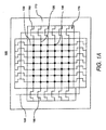
- Fig. 1A illustrates an exemplary embodiment of a memory array 100 according to the principles of the invention.
- the memory array 100 may include a substrate 110.
- the substrate 110 may be silicon or non-silicon based.
- Examples of non-silicon based substrate include materials of plastic, glass, ceramics, non-metals such as electrical insulators, and the like.
- one or more row conductors 120 and one or more column conductors 130 may be formed above the substrate 110.
- the row and column conductors 120 and 130 may extend in a row direction and column direction, respectively, to form a cross-point at each intersection.
- a memory cell 140 may be formed.
- Each memory cell 140 may be individually addressable through the respective row and column conductors 120 and 130, respectively.
- the memory cell 140 may be read-only, randomly accessible, or one-time programmable, thus allowing the memory array 100 to be a read-only memory (ROM), random access memory (RAM), or one-time programmable memory (OTP), respectively.
- ROM read-only memory
- RAM random access memory
- OTP one-time programmable memory
- the memory cell 140 may be a fuse memory cell, a fuse/diode memory cell, a fuse/anti-fuse memory cell, a magnetic memory cell, a diode memory cell, a magnetic/diode memory cell, a phase change memory cell, a resistive element cell, and the like.
- the memory array 100 may also include an array enable circuit 170.
- the array enable circuit 170 may include one or more array enable transistors 160. For example, four groups of array enable transistors 160 are shown in Fig. 1A. Each row or column conductor, 120 or 130, respectively, may be connected to one or more array enable transistors 160. For example, as shown in Fig. 1A, each row or column conductor, 120 or 130, respectively, may be connected to two array enable transistors 160 on both ends. Conduction through the row conductor 120 or the column conductor 130 is enabled or disabled through controlling the array enable transistors 160.
- the array-enable transistors 160 may be formed from microcrystalline silicon transistors, amorphous silicon transistors, or any enable switches that do not require silicon substrate.
- the memory array 100 may further include an array select line 150 connected to the array-enable transistors 160. By controlling the signal to the array select line 150, the memory array 100 may be selected or disabled. Typically, in a multiple arrays setting, a single array line 150 is dedicated to one array 100 and is not shared with any other array 100.
- Fig. 1B illustrates a second exemplary embodiment of a memory array according to the principles of the invention. As shown, only one of the ends of the row and column conductors, 120 and 130, respectively, are connected to the array enable transistors 160. Configurations other than Figs. 1A and 1B are possible without departing from the scope of the invention.
- the memory array 100 is silicon or non-silicon based, it is note worthy that the memory array need not include overhead such as sense amplifiers, output buffers, decoders, multiplexers, and the like.
- a single active circuitry layer may provide the memory location selections, sense amplifiers, and read and write controls.
- planes of memory arrays may be fabricated according to another aspect of the present invention. The planes of memory arrays then may be sorted and stacked to form a 3-D memory device, which relatively increases the storage capacity of the device.
- Fig. 2 illustrates an exemplary embodiment of a memory plane 200 according to the principles of the invention.
- the memory plane 200 may include one or more memory arrays 100, for example the memory arrays 100 of Figs. 1A and 1B, formed above the substrate 110 (not shown). Again, the substrate 110 may be silicon or non-silicon based.
- the memory plane 200 may also include one or more row buses 210 and one or more column buses 220.
- the row buses 210 may electrically connect to the row conductors 120 (not labeled) of the memory arrays 100.
- the column buses 220 may electrically to the column conductors 130 (also not labeled) of the memory arrays 100.
- an individual memory cell 140 (not shown in Fig. 2) of individual memory arrays 100 may be addressed.
- the memory plane 200 may further include a plane enable circuit 250.
- the plane enable circuit 250 may include one or more plane-enable transistors 240. For example, four groups of plane-enable transistors 240 are shown in Fig. 2. Data flow to and from the row and column buses, 210 and 220, and consequently from the memory cells 140 (not shown in Fig. 2) of the memory arrays 100 may be enabled or disabled through controlling the plane enable transistors 240.
- the plane-enable transistor 240 may be formed from microcrystalline thin-film transistor, amorphous thin-film transistor, or any enable switch that do not require silicon substrate.
- a plane select line 270 may be included in the memory plane 200, in which the plane select line 270 is connected to the plane enable transistors 240. In this manner, by controlling the signal to the plane select line 270, the memory plane 200 may be enabled or disabled.
- the memory plane 200 may yet further include one or more data side contact pads 230.
- the data side contact pads 230 may electrically connect with the row and column buses, 210 and 220, via the plane enable transistors 240.
- the memory plane 200 may be fabricated so that when multiple memory planes 200 are stacked, the data side contact pads 230 of the memory planes 200 are aligned for the next conductor process step to form data buses 310 (see Fig. 3). In this manner, the need to fabricate the interconnect vias between planes may be eliminated and the relative complexity of the device may be reduced.
- the array select line 150 of individual memory arrays 100 may come together to form a plurality of array select lines 260.
- the memory plane 200 and the active circuit plane 390 may be fabricated so that when multiple memory planes 200 are stacked together, the data side contact pads 230 are aligned that ease the interconnection of multiple memory planes and the active circuit plane.
- a deposition, plating or screening conductor process step may be used for the interconnections and to form array select bus 330 (see Fig. 3). Since the conductors of the array select bus 330 are physically wide, this process is easily accomplished.
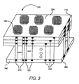
- Fig. 3 illustrates an exemplary embodiment of a memory device 300 according to the principles of the invention.
- the memory device 300 may include one or more memory planes 200 stacked to form a 3-D memory.
- the memory device 300 may also include an active circuit plane 390.
- the active circuit plane 390 may be built on a silicon substrate and may contain circuits necessary to address the memory arrays 100 of memory planes 200 including overhead elements such as address decoders, read/write control logic, sense amplifiers, output buffers, multiplexers.
- the memory device 300 may further include one or more data buses 310.
- the data buses 310 may be formed from a conductor process step to connect the aligned data side contact pads 230 (see Fig. 2) of the memory planes 200.
- the active circuit plane 390 may also include data side contact pads that are aligned and electrically connected to the data side contact pads 230 of the memory planes 200 as well.
- the memory device 300 may still further include the array select bus 330.
- the array select bus 330 may be formed from a conductor process that connect electrically the plurality of array select lines 260 through the array select side contact pads 265 on the memory planes 200 and the array select side contact pads on the active plane 390.
- the active circuit plane 390 may also include array select lines and array select side contact pads that aligned with the array select side contact pad 265 of the memory planes 200 as well.
- the memory device 300 may include a plane select bus 340.
- the plane select bus 340 may be formed from combination of the plane select lines 270 and a plane select side contact pad 275 (see Fig. 2) of individual memory planes.
- a conductor process step interconnects electrically the plane select lines 270 via the plane select side contact pad 275 on the individual memory planes 200 to the active circuit plane 390.
- Each plane 200 may have a separate plane select line 270, but the array select bus 330 may shared among the planes 200.
- Fig. 4 is a flow chart representing an exemplary method 400 to fabricate the memory device 300 of Fig. 3 according to an aspect of the present invention.
- the active circuit plane 390 may be fabricated (step 410).
- one or more memory planes 210 may be fabricated (steps 420 and 430). Note that fabricating the active circuit plane 390 may take place before, after, or simultaneously with fabricating the memory planes 200.
- the memory planes 200 may be sorted according to a predetermined error threshold (step 440).
- a threshold may be set to reject any memory plane 200 with more than 10% of the memory arrays 100 being defective.
- a tester or an electronics assembly that have read/write and control functions similar to the active circuit plane may be used.
- the screening step 440 is done at wafer probe testing stage before the wafers are diced into individual planes 200.
- a wafer may contain several planes 200.
- multiple threshold levels may be used to sort the memory planes 200. For example, it may be possible that certain applications may be able to tolerate more defects than others. In this manner, varying defect tolerance levels can be assured in the memory devices.
- the active circuit plane 390 and the memory planes 200 may be stacked and bonded with adhesive material to hold them together.
- the stacking process also aligned the side contact pads (data 230, array select 265, and plane select 275) of the memory planes 200 and the active circuit planes 390.
- the conductor process forms the plane interconnect conductors 310, 330, and 340 to make electrical connections between memory planes and the active circuit plane.
- the memory stacks are then sent through a packaging process to form the memory device 300.
Landscapes
- Engineering & Computer Science (AREA)
- Microelectronics & Electronic Packaging (AREA)
- Semiconductor Memories (AREA)
- Metal-Oxide And Bipolar Metal-Oxide Semiconductor Integrated Circuits (AREA)
- Dram (AREA)
- Read Only Memory (AREA)
Abstract
Description
Claims (10)
- A memory plane (200), comprising:a substrate (110);a plurality of array select lines (150) formed above said substrate (110);a plane-enable circuit (250) formed above said substrate (110) and configured to enable/disable said memory plane (200);a plane select line (270) electrically connected to said plane-enable circuit (250); andone or more memory arrays (100) formed above said substrate (110), wherein at least one memory array (100) includes:one or more row conductors (120) formed above said substrate (110) and extending in a row direction;one or more column conductors (130) formed above said substrate (110) and extending in a column direction such that a cross-point is formed at each intersection between said row (120) and column conductors (130);a memory cell (140) formed in one or more of said cross-points; andan array-enable circuit (170) configured to enable/disable said memory array (100) and electrically connected at least one of said plurality of array select lines (150).
- The memory plane (200) of claim 1, further comprising:a row bus (210) electrically connected to said one or more row conductors (120) of said one or more memory arrays; anda column bus (220) electrically connected to said one or more column conductors (130) of said one or more memory arrays (100).
- The memory plane (200) of claim 1, wherein said substrate (110) is silicon based and wherein each of said one or memory arrays (100) excludes sense amplifiers, output buffers, decoders, and multiplexers.
- The memory plane (200) of claim 1, wherein said substrate (110) is non-silicon based and is formed from base materials of at least one of a plastic, glass, ceramic, and non-metal.
- The memory plane (200) of claim 1, wherein said memory cell (140) includes at least one of a fuse memory cell, a fuse/diode memory cell, a fuse/anti-fuse memory cell, a magnetic memory cell, a diode memory cell, a magnetic/diode memory cell, a phase change memory cell, and a resistive element cell.
- A memory device (300), comprising:an active circuit plane (390);a data bus (310) electrically connected to said active circuit plane (390);a plane select bus (340) electrically connected to said active circuit plane (390);an array select bus (330) electrically connected to said active circuit plane (390); andone or more memory plane (200)s stacked above said active circuit plane (390), wherein at least one memory plane (200) includes:a substrate (110);a plurality of array select lines (150) formed above said substrate (110) and electrically connected to said array select bus (330);a plane-enable circuit (250) configured to enable/disable said memory plane (200);a plane select line (270) electrically connected to said plane enable-circuit (250) and to said plane select bus (340); andone or more memory arrays (100) formed above said substrate (110), wherein at least one memory array (100) includes:one or more row conductors (120)formed above said substrate (110) and extending in a row direction;one or more column conductors (130)formed above said substrate (110) and extending in a column direction such that a cross-point is formed at each intersection between said row and column conductors;a memory cell (140) formed in one or more of said cross-points; andan array-enable circuit (170) configured to enable/disable said memory array (100) and electrically connected at least one of said plurality of array select lines (150).
- The memory device (300) of claim 6, wherein said at least one memory plane (200) further comprises:a row bus (210) electrically connected to said one or more row conductors (120)of said one or more memory arrays; anda column bus (220) electrically connected to said one or more column conductors (130)of said one or more memory arrays.
- The memory device (300) of claim 7, wherein said at least one memory plane (200) further comprises at least one of:a plurality of data side contact pads (310) electrically connected to said row (210) and column (220) buses;a plurality of array select side contact pads (330) electrically connected to said array select lines (150); anda plane select side contact pad (340)n electrically connected to said plane select line (270).
- The memory device (300) of claim 8, wherein at least one of:said plurality of data side contact buses (310) are aligned and electrically connect to said data bus (310);said plurality array select side contact pads (330) are aligned and electrically connect to said array select bus (330); andsaid plane select side contact pad (340) electrically connects with a line of said plane select bus (340).
- The memory device (300) of claim 6, wherein said plurality of array select lines (150) of said memory plane (200)s are electrically connected to from said array select bus (330).
Applications Claiming Priority (2)
| Application Number | Priority Date | Filing Date | Title |
|---|---|---|---|
| US984934 | 2001-10-31 | ||
| US09/984,934 US6504742B1 (en) | 2001-10-31 | 2001-10-31 | 3-D memory device for large storage capacity |
Publications (3)
| Publication Number | Publication Date |
|---|---|
| EP1308958A2 true EP1308958A2 (en) | 2003-05-07 |
| EP1308958A3 EP1308958A3 (en) | 2003-05-14 |
| EP1308958B1 EP1308958B1 (en) | 2005-12-28 |
Family
ID=25531039
Family Applications (1)
| Application Number | Title | Priority Date | Filing Date |
|---|---|---|---|
| EP02257425A Expired - Lifetime EP1308958B1 (en) | 2001-10-31 | 2002-10-25 | Three dimensional large storage random access memory device |
Country Status (6)
| Country | Link |
|---|---|
| US (1) | US6504742B1 (en) |
| EP (1) | EP1308958B1 (en) |
| JP (1) | JP2003209222A (en) |
| KR (1) | KR100895073B1 (en) |
| CN (1) | CN1417861A (en) |
| DE (1) | DE60208310T2 (en) |
Cited By (3)
| Publication number | Priority date | Publication date | Assignee | Title |
|---|---|---|---|---|
| WO2005083715A1 (en) * | 2004-02-25 | 2005-09-09 | Micron Technology, Inc. | Multi-layer memory arrays |
| EP2172940A1 (en) * | 2008-10-07 | 2010-04-07 | Samsung Electronics Co., Ltd. | Multi-layered memory apparatus including oxide thin film transistor |
| EP2175453A1 (en) | 2008-10-10 | 2010-04-14 | Samsung Electronics Co., Ltd. | Stacked memory device and method thereof |
Families Citing this family (65)
| Publication number | Priority date | Publication date | Assignee | Title |
|---|---|---|---|---|
| EP1406187A4 (en) * | 2001-07-11 | 2007-05-02 | Riken | METHOD FOR STORING ENTITY DATA INCORPORATING FORM AND PHYSICAL QUANTITY AND STORAGE PROGRAM |
| WO2003016031A1 (en) | 2001-08-16 | 2003-02-27 | Riken | Rapid prototyping method and device using v-cad data |
| WO2003048980A1 (en) | 2001-12-04 | 2003-06-12 | Riken | Method for converting 3-dimensional shape data into cell inner data and conversion program |
| JP4320425B2 (en) | 2002-02-28 | 2009-08-26 | 独立行政法人理化学研究所 | Method and program for converting boundary data into in-cell shape |
| US6643159B2 (en) * | 2002-04-02 | 2003-11-04 | Hewlett-Packard Development Company, L.P. | Cubic memory array |
| US20040004239A1 (en) * | 2002-07-08 | 2004-01-08 | Madurawe Raminda U. | Three dimensional integrated circuits |
| US7129744B2 (en) * | 2003-10-23 | 2006-10-31 | Viciciv Technology | Programmable interconnect structures |
| US7064018B2 (en) * | 2002-07-08 | 2006-06-20 | Viciciv Technology | Methods for fabricating three dimensional integrated circuits |
| US6998722B2 (en) * | 2002-07-08 | 2006-02-14 | Viciciv Technology | Semiconductor latches and SRAM devices |
| US7064579B2 (en) * | 2002-07-08 | 2006-06-20 | Viciciv Technology | Alterable application specific integrated circuit (ASIC) |
| US7112994B2 (en) * | 2002-07-08 | 2006-09-26 | Viciciv Technology | Three dimensional integrated circuits |
| US6856030B2 (en) * | 2002-07-08 | 2005-02-15 | Viciciv Technology | Semiconductor latches and SRAM devices |
| US6828689B2 (en) * | 2002-07-08 | 2004-12-07 | Vi Ci Civ | Semiconductor latches and SRAM devices |
| US20040018711A1 (en) * | 2002-07-08 | 2004-01-29 | Madurawe Raminda U. | Methods for fabricating three dimensional integrated circuits |
| US6992503B2 (en) * | 2002-07-08 | 2006-01-31 | Viciciv Technology | Programmable devices with convertibility to customizable devices |
| US7312109B2 (en) * | 2002-07-08 | 2007-12-25 | Viciciv, Inc. | Methods for fabricating fuse programmable three dimensional integrated circuits |
| US7673273B2 (en) | 2002-07-08 | 2010-03-02 | Tier Logic, Inc. | MPGA products based on a prototype FPGA |
| US20040004251A1 (en) * | 2002-07-08 | 2004-01-08 | Madurawe Raminda U. | Insulated-gate field-effect thin film transistors |
| US8643162B2 (en) | 2007-11-19 | 2014-02-04 | Raminda Udaya Madurawe | Pads and pin-outs in three dimensional integrated circuits |
| US7812458B2 (en) * | 2007-11-19 | 2010-10-12 | Tier Logic, Inc. | Pad invariant FPGA and ASIC devices |
| US7394680B2 (en) * | 2003-03-18 | 2008-07-01 | Kabushiki Kaisha Toshiba | Resistance change memory device having a variable resistance element with a recording layer electrode served as a cation source in a write or erase mode |
| CN1759450B (en) * | 2003-03-18 | 2012-02-29 | 株式会社东芝 | Programmable Impedance Memory Device |
| US7778062B2 (en) * | 2003-03-18 | 2010-08-17 | Kabushiki Kaisha Toshiba | Resistance change memory device |
| US7400522B2 (en) * | 2003-03-18 | 2008-07-15 | Kabushiki Kaisha Toshiba | Resistance change memory device having a variable resistance element formed of a first and second composite compound for storing a cation |
| WO2004100267A1 (en) * | 2003-04-03 | 2004-11-18 | Hewlett-Packard Development Company, L.P. | Cubic memory array |
| JP4381743B2 (en) | 2003-07-16 | 2009-12-09 | 独立行政法人理化学研究所 | Method and program for generating volume data from boundary representation data |
| US6961263B2 (en) * | 2003-09-08 | 2005-11-01 | Hewlett-Packard Development Company, L.P. | Memory device with a thermally assisted write |
| US7030651B2 (en) | 2003-12-04 | 2006-04-18 | Viciciv Technology | Programmable structured arrays |
| US7176713B2 (en) * | 2004-01-05 | 2007-02-13 | Viciciv Technology | Integrated circuits with RAM and ROM fabrication options |
| JP4399777B2 (en) * | 2004-01-21 | 2010-01-20 | セイコーエプソン株式会社 | Semiconductor memory device, semiconductor device, and electronic device |
| KR100564611B1 (en) * | 2004-02-14 | 2006-03-29 | 삼성전자주식회사 | Hard disk drive buffer structure |
| US7489164B2 (en) * | 2004-05-17 | 2009-02-10 | Raminda Udaya Madurawe | Multi-port memory devices |
| JP4662740B2 (en) | 2004-06-28 | 2011-03-30 | 日本電気株式会社 | Stacked semiconductor memory device |
| US7589368B2 (en) * | 2005-03-21 | 2009-09-15 | Micronix International Co., Ltd. | Three-dimensional memory devices |
| US7359279B2 (en) | 2005-03-31 | 2008-04-15 | Sandisk 3D Llc | Integrated circuit memory array configuration including decoding compatibility with partial implementation of multiple memory layers |
| JP4783100B2 (en) | 2005-09-12 | 2011-09-28 | 独立行政法人理化学研究所 | Method of converting boundary data into in-cell shape data and its conversion program |
| KR100855861B1 (en) * | 2005-12-30 | 2008-09-01 | 주식회사 하이닉스반도체 | Nonvolatile Semiconductor Memory Device |
| US20070183189A1 (en) * | 2006-02-08 | 2007-08-09 | Thomas Nirschl | Memory having nanotube transistor access device |
| US7486111B2 (en) * | 2006-03-08 | 2009-02-03 | Tier Logic, Inc. | Programmable logic devices comprising time multiplexed programmable interconnect |
| US7345899B2 (en) * | 2006-04-07 | 2008-03-18 | Infineon Technologies Ag | Memory having storage locations within a common volume of phase change material |
| JP2007322141A (en) * | 2006-05-30 | 2007-12-13 | Yokogawa Electric Corp | Semiconductor integrated circuit test apparatus and method |
| JP2008140220A (en) * | 2006-12-04 | 2008-06-19 | Nec Corp | Semiconductor device |
| US7692951B2 (en) * | 2007-06-12 | 2010-04-06 | Kabushiki Kaisha Toshiba | Resistance change memory device with a variable resistance element formed of a first and a second composite compound |
| US8679977B2 (en) * | 2007-07-25 | 2014-03-25 | Micron Technology, Inc. | Method and apparatus providing multi-planed array memory device |
| US7898893B2 (en) * | 2007-09-12 | 2011-03-01 | Samsung Electronics Co., Ltd. | Multi-layered memory devices |
| KR101330710B1 (en) | 2007-11-01 | 2013-11-19 | 삼성전자주식회사 | Flash memory device |
| US20090128189A1 (en) * | 2007-11-19 | 2009-05-21 | Raminda Udaya Madurawe | Three dimensional programmable devices |
| US7635988B2 (en) * | 2007-11-19 | 2009-12-22 | Tier Logic, Inc. | Multi-port thin-film memory devices |
| US7573293B2 (en) * | 2007-12-26 | 2009-08-11 | Tier Logic, Inc. | Programmable logic based latches and shift registers |
| US7602213B2 (en) * | 2007-12-26 | 2009-10-13 | Tier Logic, Inc. | Using programmable latch to implement logic |
| US7795913B2 (en) * | 2007-12-26 | 2010-09-14 | Tier Logic | Programmable latch based multiplier |
| US7573294B2 (en) * | 2007-12-26 | 2009-08-11 | Tier Logic, Inc. | Programmable logic based latches and shift registers |
| US8230375B2 (en) | 2008-09-14 | 2012-07-24 | Raminda Udaya Madurawe | Automated metal pattern generation for integrated circuits |
| US8023307B1 (en) | 2010-04-30 | 2011-09-20 | Hewlett-Packard Development Company, L.P. | Peripheral signal handling in extensible three dimensional circuits |
| US8159265B1 (en) | 2010-11-16 | 2012-04-17 | Raminda Udaya Madurawe | Memory for metal configurable integrated circuits |
| US8159268B1 (en) | 2010-11-16 | 2012-04-17 | Raminda Udaya Madurawe | Interconnect structures for metal configurable integrated circuits |
| US8159266B1 (en) | 2010-11-16 | 2012-04-17 | Raminda Udaya Madurawe | Metal configurable integrated circuits |
| TWI564890B (en) * | 2011-01-26 | 2017-01-01 | 半導體能源研究所股份有限公司 | Memory device and semiconductor device |
| JP6081171B2 (en) | 2011-12-09 | 2017-02-15 | 株式会社半導体エネルギー研究所 | Storage device |
| US9117503B2 (en) * | 2012-08-29 | 2015-08-25 | Micron Technology, Inc. | Memory array plane select and methods |
| US20150287706A1 (en) * | 2012-10-24 | 2015-10-08 | Mitsunari Sukekawa | Semiconductor device and method for manufacturing the same |
| CN103022071B (en) * | 2012-12-13 | 2015-06-17 | 南京大学 | Flexible storage and manufacture method |
| CN106920797B (en) * | 2017-03-08 | 2018-10-12 | 长江存储科技有限责任公司 | Memory construction and preparation method thereof, the test method of memory |
| US10833059B2 (en) * | 2018-12-07 | 2020-11-10 | Micron Technology, Inc. | Integrated assemblies comprising vertically-stacked decks of memory arrays |
| EP4332973B1 (en) | 2020-02-20 | 2025-05-14 | Yangtze Memory Technologies Co., Ltd. | Method of programming multi-plane memory device |
Family Cites Families (12)
| Publication number | Priority date | Publication date | Assignee | Title |
|---|---|---|---|---|
| JPS6220043A (en) * | 1985-07-19 | 1987-01-28 | Yukihiro Taguchi | Random access memory capable of asynchronous simultaneous access for multiprocessor |
| JPH06167958A (en) * | 1991-03-28 | 1994-06-14 | Texas Instr Inc <Ti> | Memory device |
| US5397726A (en) * | 1992-02-04 | 1995-03-14 | National Semiconductor Corporation | Segment-erasable flash EPROM |
| US5786629A (en) * | 1992-05-14 | 1998-07-28 | Reveo, Inc. | 3-D packaging using massive fillo-leaf technology |
| JPH0793997A (en) * | 1993-09-24 | 1995-04-07 | Nec Corp | Static semiconductor memory device |
| EP1178530A2 (en) * | 1993-09-30 | 2002-02-06 | Kopin Corporation | Three-dimensional processor using transferred thin film circuits |
| US6157356A (en) * | 1996-04-12 | 2000-12-05 | International Business Machines Company | Digitally driven gray scale operation of active matrix OLED displays |
| NO308149B1 (en) * | 1998-06-02 | 2000-07-31 | Thin Film Electronics Asa | Scalable, integrated data processing device |
| JP4085459B2 (en) * | 1998-03-02 | 2008-05-14 | セイコーエプソン株式会社 | Manufacturing method of three-dimensional device |
| US6034882A (en) * | 1998-11-16 | 2000-03-07 | Matrix Semiconductor, Inc. | Vertically stacked field programmable nonvolatile memory and method of fabrication |
| KR100301932B1 (en) * | 1999-04-27 | 2001-10-29 | 윤종용 | A non-volatile semiconductor memory device |
| TW587252B (en) * | 2000-01-18 | 2004-05-11 | Hitachi Ltd | Semiconductor memory device and data processing device |
-
2001
- 2001-10-31 US US09/984,934 patent/US6504742B1/en not_active Expired - Lifetime
-
2002
- 2002-10-25 EP EP02257425A patent/EP1308958B1/en not_active Expired - Lifetime
- 2002-10-25 DE DE60208310T patent/DE60208310T2/en not_active Expired - Lifetime
- 2002-10-30 KR KR1020020066377A patent/KR100895073B1/en not_active Expired - Fee Related
- 2002-10-31 CN CN02148159A patent/CN1417861A/en active Pending
- 2002-10-31 JP JP2002317262A patent/JP2003209222A/en active Pending
Cited By (7)
| Publication number | Priority date | Publication date | Assignee | Title |
|---|---|---|---|---|
| WO2005083715A1 (en) * | 2004-02-25 | 2005-09-09 | Micron Technology, Inc. | Multi-layer memory arrays |
| US7112815B2 (en) | 2004-02-25 | 2006-09-26 | Micron Technology, Inc. | Multi-layer memory arrays |
| US7157305B2 (en) | 2004-02-25 | 2007-01-02 | Micron Technology, Inc. | Forming multi-layer memory arrays |
| EP2172940A1 (en) * | 2008-10-07 | 2010-04-07 | Samsung Electronics Co., Ltd. | Multi-layered memory apparatus including oxide thin film transistor |
| CN101714404A (en) * | 2008-10-07 | 2010-05-26 | 三星电子株式会社 | Multi-layered memory apparatus comprising oxide thin film transistor |
| EP2175453A1 (en) | 2008-10-10 | 2010-04-14 | Samsung Electronics Co., Ltd. | Stacked memory device and method thereof |
| US8547719B2 (en) | 2008-10-10 | 2013-10-01 | Samsung Electronics Co., Ltd. | Stacked memory device and method thereof |
Also Published As
| Publication number | Publication date |
|---|---|
| KR100895073B1 (en) | 2009-04-27 |
| DE60208310D1 (en) | 2006-02-02 |
| EP1308958A3 (en) | 2003-05-14 |
| DE60208310T2 (en) | 2006-07-27 |
| CN1417861A (en) | 2003-05-14 |
| EP1308958B1 (en) | 2005-12-28 |
| US6504742B1 (en) | 2003-01-07 |
| JP2003209222A (en) | 2003-07-25 |
| KR20030036028A (en) | 2003-05-09 |
Similar Documents
| Publication | Publication Date | Title |
|---|---|---|
| EP1308958B1 (en) | Three dimensional large storage random access memory device | |
| US12170126B2 (en) | Stacked DRAM device and method of manufacture | |
| US20230050150A1 (en) | Stacked architecture for three-dimensional nand | |
| US8040745B2 (en) | Stacked memory and fuse chip | |
| US8866303B2 (en) | Semiconductor device with configurable through-silicon vias | |
| US6774458B2 (en) | Vertical interconnection structure and methods | |
| TWI281672B (en) | Three-dimensional semiconductor device provided with interchip interconnection selection means for electrically isolating interconnections other than selected interchip interconnections | |
| CN101261945A (en) | Fabrication method of semiconductor structure | |
| JP2009506476A (en) | Self-identifying multilayer die semiconductor components | |
| CN1518797A (en) | On-die antifuse rerouting | |
| US11276669B2 (en) | High capacity semiconductor device including bifurcated memory module | |
| US20130168674A1 (en) | Methods and Systems for Repairing Interior Device Layers in Three-Dimensional Integrated Circuits | |
| JP2011100898A (en) | Semiconductor device | |
| CN114512490B (en) | A memory and a method for preparing the same | |
| US11599484B2 (en) | Semiconductor device having plural signal buses for multiple purposes | |
| CN120379255A (en) | High capacity high bandwidth non-volatile memory device |
Legal Events
| Date | Code | Title | Description |
|---|---|---|---|
| PUAI | Public reference made under article 153(3) epc to a published international application that has entered the european phase |
Free format text: ORIGINAL CODE: 0009012 |
|
| PUAL | Search report despatched |
Free format text: ORIGINAL CODE: 0009013 |
|
| AK | Designated contracting states |
Designated state(s): AT BE BG CH CY CZ DE DK EE ES FI FR GB GR IE IT LI LU MC NL PT SE SK TR |
|
| AX | Request for extension of the european patent |
Extension state: AL LT LV MK RO SI |
|
| AK | Designated contracting states |
Designated state(s): AT BE BG CH CY CZ DE DK EE ES FI FR GB GR IE IT LI LU MC NL PT SE SK TR |
|
| AX | Request for extension of the european patent |
Extension state: AL LT LV MK RO SI |
|
| RIC1 | Information provided on ipc code assigned before grant |
Ipc: 7H 01L 25/065 B Ipc: 7G 11C 8/12 A Ipc: 7H 01L 21/822 B |
|
| 17P | Request for examination filed |
Effective date: 20031028 |
|
| 17Q | First examination report despatched |
Effective date: 20031217 |
|
| AKX | Designation fees paid |
Designated state(s): DE GB |
|
| GRAP | Despatch of communication of intention to grant a patent |
Free format text: ORIGINAL CODE: EPIDOSNIGR1 |
|
| GRAS | Grant fee paid |
Free format text: ORIGINAL CODE: EPIDOSNIGR3 |
|
| GRAA | (expected) grant |
Free format text: ORIGINAL CODE: 0009210 |
|
| AK | Designated contracting states |
Kind code of ref document: B1 Designated state(s): DE GB |
|
| REG | Reference to a national code |
Ref country code: GB Ref legal event code: FG4D |
|
| REF | Corresponds to: |
Ref document number: 60208310 Country of ref document: DE Date of ref document: 20060202 Kind code of ref document: P |
|
| PLBE | No opposition filed within time limit |
Free format text: ORIGINAL CODE: 0009261 |
|
| STAA | Information on the status of an ep patent application or granted ep patent |
Free format text: STATUS: NO OPPOSITION FILED WITHIN TIME LIMIT |
|
| 26N | No opposition filed |
Effective date: 20060929 |
|
| REG | Reference to a national code |
Ref country code: GB Ref legal event code: 732E |
|
| PGFP | Annual fee paid to national office [announced via postgrant information from national office to epo] |
Ref country code: GB Payment date: 20210915 Year of fee payment: 20 |
|
| PGFP | Annual fee paid to national office [announced via postgrant information from national office to epo] |
Ref country code: DE Payment date: 20210914 Year of fee payment: 20 |
|
| REG | Reference to a national code |
Ref country code: DE Ref legal event code: R071 Ref document number: 60208310 Country of ref document: DE |
|
| REG | Reference to a national code |
Ref country code: GB Ref legal event code: PE20 Expiry date: 20221024 |
|
| PG25 | Lapsed in a contracting state [announced via postgrant information from national office to epo] |
Ref country code: GB Free format text: LAPSE BECAUSE OF EXPIRATION OF PROTECTION Effective date: 20221024 |