EP1308817A2 - Function circuit that is less prone to be affected by temperature - Google Patents
Function circuit that is less prone to be affected by temperature Download PDFInfo
- Publication number
- EP1308817A2 EP1308817A2 EP02023291A EP02023291A EP1308817A2 EP 1308817 A2 EP1308817 A2 EP 1308817A2 EP 02023291 A EP02023291 A EP 02023291A EP 02023291 A EP02023291 A EP 02023291A EP 1308817 A2 EP1308817 A2 EP 1308817A2
- Authority
- EP
- European Patent Office
- Prior art keywords
- transistor
- circuit
- function circuit
- base
- function
- Prior art date
- Legal status (The legal status is an assumption and is not a legal conclusion. Google has not performed a legal analysis and makes no representation as to the accuracy of the status listed.)
- Withdrawn
Links
- 238000010586 diagram Methods 0.000 description 8
- 230000012447 hatching Effects 0.000 description 1
- 238000012886 linear function Methods 0.000 description 1
Images




Classifications
-
- G—PHYSICS
- G05—CONTROLLING; REGULATING
- G05F—SYSTEMS FOR REGULATING ELECTRIC OR MAGNETIC VARIABLES
- G05F3/00—Non-retroactive systems for regulating electric variables by using an uncontrolled element, or an uncontrolled combination of elements, such element or such combination having self-regulating properties
- G05F3/02—Regulating voltage or current
- G05F3/08—Regulating voltage or current wherein the variable is DC
-
- G—PHYSICS
- G05—CONTROLLING; REGULATING
- G05F—SYSTEMS FOR REGULATING ELECTRIC OR MAGNETIC VARIABLES
- G05F3/00—Non-retroactive systems for regulating electric variables by using an uncontrolled element, or an uncontrolled combination of elements, such element or such combination having self-regulating properties
- G05F3/02—Regulating voltage or current
- G05F3/08—Regulating voltage or current wherein the variable is DC
- G05F3/10—Regulating voltage or current wherein the variable is DC using uncontrolled devices with non-linear characteristics
- G05F3/16—Regulating voltage or current wherein the variable is DC using uncontrolled devices with non-linear characteristics being semiconductor devices
- G05F3/20—Regulating voltage or current wherein the variable is DC using uncontrolled devices with non-linear characteristics being semiconductor devices using diode- transistor combinations
- G05F3/22—Regulating voltage or current wherein the variable is DC using uncontrolled devices with non-linear characteristics being semiconductor devices using diode- transistor combinations wherein the transistors are of the bipolar type only
- G05F3/222—Regulating voltage or current wherein the variable is DC using uncontrolled devices with non-linear characteristics being semiconductor devices using diode- transistor combinations wherein the transistors are of the bipolar type only with compensation for device parameters, e.g. Early effect, gain, manufacturing process, or external variations, e.g. temperature, loading, supply voltage
- G05F3/225—Regulating voltage or current wherein the variable is DC using uncontrolled devices with non-linear characteristics being semiconductor devices using diode- transistor combinations wherein the transistors are of the bipolar type only with compensation for device parameters, e.g. Early effect, gain, manufacturing process, or external variations, e.g. temperature, loading, supply voltage producing a current or voltage as a predetermined function of the temperature
-
- G—PHYSICS
- G05—CONTROLLING; REGULATING
- G05F—SYSTEMS FOR REGULATING ELECTRIC OR MAGNETIC VARIABLES
- G05F3/00—Non-retroactive systems for regulating electric variables by using an uncontrolled element, or an uncontrolled combination of elements, such element or such combination having self-regulating properties
- G05F3/02—Regulating voltage or current
- G05F3/08—Regulating voltage or current wherein the variable is DC
- G05F3/10—Regulating voltage or current wherein the variable is DC using uncontrolled devices with non-linear characteristics
- G05F3/16—Regulating voltage or current wherein the variable is DC using uncontrolled devices with non-linear characteristics being semiconductor devices
- G05F3/20—Regulating voltage or current wherein the variable is DC using uncontrolled devices with non-linear characteristics being semiconductor devices using diode- transistor combinations
- G05F3/26—Current mirrors
- G05F3/265—Current mirrors using bipolar transistors only
Definitions
- the present invention relates to a function circuit for converting an input signal into an output signal by a prescribed function.
- the invention relates to a function circuit that is less prone to be affected by temperature.
- Fig. 5 is a circuit diagram of a conventional function circuit.
- Fig. 6 shows an input/output characteristic of the circuit of Fig. 5.
- the function circuit of Fig. 5 is composed of three resistors R1, R2, and R3, two diodes D1 and D2, and two reference supply voltages V1 and V2.
- the resistor R2, the diode D1, and the reference supply voltage V2 are connected to each other in series and the resistor R3, the diode D2, and the reference supply voltage V1 are also connected to each other in series.
- the resistor R1 is connected to the resistors R2 and R3.
- One end of the resistor R1 is an input terminal IN and the other end (connecting point) is an output terminal OUT of the function circuit.
- the diode D2 is opposite in direction to the diode D1.
- An input signal Vs is input to the input terminal IN.
- the reference supply voltage V1 is 2 V and the reference supply voltage V2 is 3 V.
- the horizontal axis represents the input signal Vs that is input to the input terminal IN and the vertical axis represents the output signal Vout at the output terminal OUT of the function circuit.
- each of Vs and Vout is in the range of 0 V to 5 V.
- two change points ⁇ and ⁇ where linear lines having different slopes are connected to each other smoothly appear in the vicinity of the voltages 2 V and 3 V (reference supply voltages V1 and V2), respectively.
- a generally S-shaped curve can be formed that is bent at the change points ⁇ and ⁇ that are in the vicinity of 2 V and 3 V.
- Vout shown in Fig. 5 can be given by. the following formulae, where Vd is the forward voltage of the diodes D1 and D2:
- Fig. 7 is a circuit diagram of another conventional function circuit.
- Fig. 8 shows an input/output characteristic of the function circuit of Fig. 7.
- the function circuit of Fig. 7 is mainly composed of a first circuit including an npn transistor Q1 and a pnp transistor Q2 and a second circuit including a pnp transistor Q3 and an npn transistor Q4.
- the base terminal of the transistor Q1 and the emitter terminal of the transistor Q2 are connected to each other.
- the base terminal of the transistor Q3 and the emitter terminal of the transistor Q4 are connected to each other.
- One end of a resistor R1 is connected to the connecting point P1 of the resistors R2 and R3.
- the other end of the resistor R1 serves as an input terminal IN to which an input signal Vs is input.
- a reference supply voltage V1 (2V) is applied to the base terminal of the transistor Q2, and a reference supply voltage V2 (3 V) is applied to the base terminal of the transistor Q4.
- the connecting point P1 also serves as an output terminal OUT.
- the potential of the emitter terminal of the transistor Q2 is set higher than the reference supply voltage V1 (2 V) that is applied to the base terminal of the transistor Q2 by the base-emitter voltage Vbe of the transistor Q2.
- the potential of the emitter terminal of the transistor Q1 is set lower than the emitter potential of the transistor Q2 by the base-emitter voltage Vbe of the transistor Q1. Therefore, the base-emitter voltage Vbe of the transistor Q2 and the base-emitter voltage Vbe of the transistor Q1 are in a relationship that they cancel out each other.
- the potential of the base terminal of the transistor Q2 and the potential of the emitter terminal of the transistor Q1 are set identical.
- the function circuit of Fig. 7 has an input/output characteristic having a curve that is centered at 2.5 V (Vcc/2) and is bent in the vicinity of the reference voltage V1 (change point ⁇ ) and the reference voltage V2 (change point ⁇ ).
- the output signal Vout is given by the following formulae:
- the function circuit of Fig. 5 uses the diodes D1 and D2.
- diodes have a characteristic that the forward voltage Vd tends to vary with temperature.
- the formula representing the output signal Vout includes the forward voltage Vd. Therefore, errors indicated by hatching in Fig. 6 occur in the ranges of Vs ⁇ V1 + Vd and Vs ⁇ V2 - Vd because the diode forward voltage Vd varies being affected by a temperature variation.
- the present invention has been made to solve the above problems, and an object of the invention is therefore to provide a function circuit that is less prone to be affected by temperature.
- the invention provides a function circuit for converting an input signal by a prescribed function, comprising a first transistor; a second transistor; voltage dividing means connected to the first transistor, for dividing the input signal with a prescribed division ratio; a reference voltage source for applying a prescribed reference voltage to a base terminal of the second transistor; and a current mirror circuit that is connected to the first transistor and the second transistor so that the same constant current flows between a collector terminal and an emitter terminal of the first transistor and between those of the second transistor.
- a first function circuit is such that the first transistor is a pnp transistor and the second transistor is an npn transistor.
- a second function circuit is such that the first transistor is an npn transistor and the second transistor is a pnp transistor.
- a function circuit may be formed by using at least one pair of the first function circuit and the second function circuit, at least one first function circuit, or at least one second function circuit.
- the use of the current mirror circuit makes it possible to allow the same base current to flow through the paired npn transistor and pnp transistor. Therefore, their base-emitter voltages Vbe can be made identical and can cancel out each other sufficiently even with a temperature variation. As a result, the function circuit is not affected by temperature.
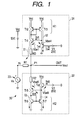
- Fig. 1 is a circuit diagram of a function circuit 30 according to the invention.
- Fig. 2 shows an input/output characteristic of the function circuit of Fig. 1.
- the function circuit 30 of Fig. 1 is mainly composed of a first circuit 31 and a second circuit 32.
- the first circuit 31 is composed of transistors Tr2 and Tr3 that constitute a current mirror circuit K1, an npn transistor Tr1 that is provided on the input side of the current mirror circuit K1, a pnp transistor Tr4 that is provided on the output side of the current mirror circuit K1 and serves as an active load, a resistor R3 that is connected to the emitter terminal of the transistor Tr1, and a reference supply voltage V1 that is applied to the base terminal of the transistor Tr4.
- the second circuit 32 is composed of transistors Tr6 and Tr7 that constitute a current mirror circuit K2, a pnp transistor Tr5 that is provided on the input side of the current mirror circuit K2, an npn transistor Tr8 that is provided on the output side of the current mirror circuit K2 and serves as an active load, a resistor R2 that is connected to the emitter terminal of the transistor Tr5, and a reference supply voltage V2 that is applied to the base terminal of the transistor Tr8.
- the resistor R3 of the first circuit 31 and the resistor R2 of the second circuit 32 are connected to each other, and an input signal Vs is applied to the connecting point P1 of the resistors R2 and R3 via a resistor R1.
- the operation of the function circuit 30 will be described below. More specifically, an exemplary operation of the function circuit 30 will be described with an assumption that the supply voltage Vcc is set at 5 V and the change point reference voltages V1 and V2 are set at 2 V and 3 V, respectively.
- the potential of the emitter terminal of the transistor Tr4 and the potential of the base terminal of the transistor Tr1 are set higher than the reference voltage V1 by the base-emitter voltage Vbe4 of the transistor Tr4.
- the potential of the emitter terminal of the transistor Tr1 is set lower than the base potential of the transistor Tr1 by the base-emitter voltage Vbe1 of the transistor Tr1. Therefore, the emitter potential of the transistor Tr1 is approximately equal to the base potential of the transistor Tr4.
- the transistor Tr5 is off, that is, in a high-impedance state. Therefore, the second circuit 32 does not cause any influences on the output signal Vout of the function circuit 30.
- the transistors Tr5 and Tr8 of the second circuit 32 are a pnp transistor and an npn transistor, respectively.
- the potential of the emitter terminal of the transistor Tr5 is set higher than the base potential of the transistor Tr5 by the base-emitter voltage Vbe5 pof the transistor Tr5. Therefore, the emitter potential of the transistor Tr5 is set approximately equal to the base potential (3 V) of the transistor Tr8.
- the transistor Tr1 is off, that is, in a high-impedance state. Therefore, the first circuit 31 does not cause any influences on the output signal Vout of the function circuit 30.
- Vout Vs
- the slopes of the straight lines of Formulae (7) and (8) can easily be set in accordance with the ratio among the resistances R1, R2, and R3.
- the transistor base-emitter voltages Vbe can cancel out each other sufficiently, no influences are caused by variations in the diode forward voltages Vd or the transistor base-emitter voltages Vbe due to a temperature variation.
- Fig. 3 is a circuit diagram of a function circuit 40 that is a combination of function circuits shown in Fig. 1.
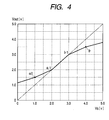
- Fig. 4 is an input/output characteristic of the function circuit 40 of Fig. 3.
- the function circuit 40 of Fig. 3 is such that two circuits each being the main circuit of the function circuit 30 shown in Fig. 1, except for the voltage source circuit, are connected to each other. More specifically, a third circuit 41 that is the same as the first circuit 31 and a'fourth circuit 42 that is the same as the second circuit 32 are connected to the function circuit 30. However, reference voltages V3 and V4 of the third circuit 41 and the fourth circuit 42 are different from the reference voltages V1 and V2 of the first circuit 31 and the second circuit 32, respectively. For example, the reference voltages V3 and V4 are set at 1 V and 4 V, respectively.
- the resistance division ratios R2/(R1 + R2) and R1/(R1 + R3) are set at prescribed values.
- the number of change points can be increased by combining a plurality of circuits each being the main part of the function circuit 30 of Fig. 1 in the above-described manner.
- An arbitrary function circuit can be obtained by connecting linear functions at those change points.
- the above function circuits employ the first circuit and the second circuit in the form of a pair, the invention is not limited to such a case. Only a plurality of first circuits or only a plurality of second circuits may be combined together. Even in the case of combining first circuits and second circuits, the first circuits and the second circuits need not be used in the same number. Desired function circuits can be formed by combining first circuits and second circuits in various manners.
- an input signal can be converted into an output signal by a desired function circuit without being affected by temperature.
Landscapes
- Engineering & Computer Science (AREA)
- Physics & Mathematics (AREA)
- Microelectronics & Electronic Packaging (AREA)
- Electromagnetism (AREA)
- General Physics & Mathematics (AREA)
- Radar, Positioning & Navigation (AREA)
- Automation & Control Theory (AREA)
- Nonlinear Science (AREA)
- Amplifiers (AREA)
- Measuring Temperature Or Quantity Of Heat (AREA)
Abstract
Description
Claims (4)
- A function circuit for converting an input signal by a prescribed function, comprising:a first transistor;a second transistor;voltage dividing means connected to the first transistor, for dividing the input signal with a prescribed division ratio;a reference voltage source for applying a prescribed reference voltage to a base terminal of the second transistor; anda current mirror circuit that is connected to the first transistor and the second transistor so that the same constant current flows between a collector terminal and an emitter terminal of the first transistor and between those of the second transistor.
- The function circuit according to claim 1, wherein the first transistor is a pnp transistor and the second transistor is an npn transistor.
- The function circuit according to claim 1, wherein the first transistor is an npn transistor and the second transistor is a pnp transistor.
- A function circuit for converting an input signal by a prescribed function, including at least one pair of a first function circuit and a second function circuit each comprising:wherein the first transistor of the first function circuit is a pnp transistor, the second transistor of the first function circuit is an npn transistor, the first transistor of the second function circuit is an npn transistor and the second transistor of the second function circuit is a pnp transistor.a first transistor;a second transistor;voltage dividing means connected to the first transistor, for dividing the input signal with a prescribed division ratio;a reference voltage source for applying a prescribed reference voltage to a base terminal of the second transistor; anda current mirror circuit that is connected to the first transistor and the second transistor so that the same constant current flows between a collector terminal and an emitter terminal of the first transistor and between those of the second transistor,
Applications Claiming Priority (2)
| Application Number | Priority Date | Filing Date | Title |
|---|---|---|---|
| JP2001324765 | 2001-10-23 | ||
| JP2001324765 | 2001-10-23 |
Publications (2)
| Publication Number | Publication Date |
|---|---|
| EP1308817A2 true EP1308817A2 (en) | 2003-05-07 |
| EP1308817A3 EP1308817A3 (en) | 2004-10-13 |
Family
ID=19141440
Family Applications (1)
| Application Number | Title | Priority Date | Filing Date |
|---|---|---|---|
| EP02023291A Withdrawn EP1308817A3 (en) | 2001-10-23 | 2002-10-17 | Function circuit that is less prone to be affected by temperature |
Country Status (3)
| Country | Link |
|---|---|
| US (1) | US6642772B2 (en) |
| EP (1) | EP1308817A3 (en) |
| KR (1) | KR20030033929A (en) |
Cited By (1)
| Publication number | Priority date | Publication date | Assignee | Title |
|---|---|---|---|---|
| WO2006079978A3 (en) * | 2005-01-28 | 2007-09-13 | Nxp Bv | Voltage integrator and transformer provided with such an integrator |
Family Cites Families (14)
| Publication number | Priority date | Publication date | Assignee | Title |
|---|---|---|---|---|
| US4223280A (en) * | 1979-01-19 | 1980-09-16 | Rca Corporation | Relaxation oscillator including an SCR and having switch means for interrupting current flow therethrough |
| US4604532A (en) * | 1983-01-03 | 1986-08-05 | Analog Devices, Incorporated | Temperature compensated logarithmic circuit |
| US4730124A (en) * | 1987-02-11 | 1988-03-08 | Tektronix, Inc. | High transconductance composite PNP transistor |
| JPH02309717A (en) * | 1989-05-24 | 1990-12-25 | Matsushita Electric Ind Co Ltd | Temperature characteristic correction circuit |
| US5471132A (en) * | 1991-09-30 | 1995-11-28 | Sgs-Thomson Microelectronics, Inc. | Logarithmic and exponential converter circuits |
| GB2284719B (en) * | 1993-12-13 | 1998-03-11 | Nec Corp | Differential circuit capable of accomplishing a desirable characteritic |
| DE19581856B3 (en) * | 1994-11-09 | 2013-08-29 | That Corp. | Temperature compensation for integrated circuit devices at the die level |
| US5793247A (en) * | 1994-12-16 | 1998-08-11 | Sgs-Thomson Microelectronics, Inc. | Constant current source with reduced sensitivity to supply voltage and process variation |
| JPH08202463A (en) | 1995-01-24 | 1996-08-09 | Fujitsu Ltd | Reference power supply circuit |
| US5714902A (en) * | 1995-11-30 | 1998-02-03 | Oak Crystal, Inc. | Polynomial function generation circuit |
| US5825168A (en) * | 1997-06-13 | 1998-10-20 | Vtc, Inc. | High performance maximum and minimum circuit |
| US6069520A (en) * | 1997-07-09 | 2000-05-30 | Denso Corporation | Constant current circuit using a current mirror circuit and its application |
| KR100285503B1 (en) * | 1997-12-24 | 2001-04-02 | 이계철 | Fuzzy Membership Electronic Circuit Using Linear Resistance and Switch |
| US6433624B1 (en) * | 2000-11-30 | 2002-08-13 | Intel Corporation | Threshold voltage generation circuit |
-
2002
- 2002-10-15 US US10/272,591 patent/US6642772B2/en not_active Expired - Lifetime
- 2002-10-15 KR KR1020020062906A patent/KR20030033929A/en not_active Ceased
- 2002-10-17 EP EP02023291A patent/EP1308817A3/en not_active Withdrawn
Cited By (1)
| Publication number | Priority date | Publication date | Assignee | Title |
|---|---|---|---|---|
| WO2006079978A3 (en) * | 2005-01-28 | 2007-09-13 | Nxp Bv | Voltage integrator and transformer provided with such an integrator |
Also Published As
| Publication number | Publication date |
|---|---|
| US20030076151A1 (en) | 2003-04-24 |
| KR20030033929A (en) | 2003-05-01 |
| EP1308817A3 (en) | 2004-10-13 |
| US6642772B2 (en) | 2003-11-04 |
Similar Documents
| Publication | Publication Date | Title |
|---|---|---|
| JP3772300B2 (en) | Micropower RC oscillator | |
| US6429700B1 (en) | Driver circuit with output common mode voltage control | |
| JPS6093530A (en) | Constant current source circuit | |
| JPH0695610B2 (en) | Bias voltage generating circuit and method thereof | |
| EP0083208B1 (en) | A bias circuit for an emitter coupled logic circuit | |
| JP2869664B2 (en) | Current amplifier | |
| US6903609B2 (en) | Operational amplifier | |
| US6642772B2 (en) | Function circuit that is less prone to be affected by temperature | |
| JP3643389B2 (en) | Constant voltage circuit | |
| EP0110720B1 (en) | Current mirror circuit | |
| JPS63214009A (en) | Composite transistor | |
| JP4130856B2 (en) | Current source circuit | |
| JPH0669140B2 (en) | Level shift circuit | |
| JP3323983B2 (en) | Constant current source circuit | |
| JP3088336B2 (en) | Frequency conversion circuit | |
| JP2003204232A (en) | Function circuit | |
| JP2002064337A (en) | Amplifier circuit | |
| JPH0498683A (en) | Differential amplifier circuit | |
| JPS6182521A (en) | Differential type comparator circuit | |
| JP3076129B2 (en) | Differential amplifier | |
| GB2332110A (en) | Voltage level shift circuit | |
| JPH06260925A (en) | Level shift circuit | |
| JPS6211375B2 (en) | ||
| JPH07109979B2 (en) | Schmidt circuit | |
| JPH04338811A (en) | Generating circuit for band gap reference voltage |
Legal Events
| Date | Code | Title | Description |
|---|---|---|---|
| PUAI | Public reference made under article 153(3) epc to a published international application that has entered the european phase |
Free format text: ORIGINAL CODE: 0009012 |
|
| AK | Designated contracting states |
Designated state(s): AT BE BG CH CY CZ DE DK EE ES FI FR GB GR IE IT LI LU MC NL PT SE SK TR |
|
| AX | Request for extension of the european patent |
Extension state: AL LT LV MK RO SI |
|
| PUAL | Search report despatched |
Free format text: ORIGINAL CODE: 0009013 |
|
| AK | Designated contracting states |
Kind code of ref document: A3 Designated state(s): AT BE BG CH CY CZ DE DK EE ES FI FR GB GR IE IT LI LU MC NL PT SE SK TR |
|
| AX | Request for extension of the european patent |
Extension state: AL LT LV MK RO SI |
|
| AKX | Designation fees paid | ||
| REG | Reference to a national code |
Ref country code: DE Ref legal event code: 8566 |
|
| STAA | Information on the status of an ep patent application or granted ep patent |
Free format text: STATUS: THE APPLICATION IS DEEMED TO BE WITHDRAWN |
|
| 18D | Application deemed to be withdrawn |
Effective date: 20050503 |