EP1308544A1 - SILICON SINGLE CRYSTAL WAFER HAVING VOID DENUDED ZONE ON THE SUFRACE AND DIAMETER OF ABOVE 300 mm AND ITS PRODUCTION METHOD - Google Patents
SILICON SINGLE CRYSTAL WAFER HAVING VOID DENUDED ZONE ON THE SUFRACE AND DIAMETER OF ABOVE 300 mm AND ITS PRODUCTION METHOD Download PDFInfo
- Publication number
- EP1308544A1 EP1308544A1 EP02736029A EP02736029A EP1308544A1 EP 1308544 A1 EP1308544 A1 EP 1308544A1 EP 02736029 A EP02736029 A EP 02736029A EP 02736029 A EP02736029 A EP 02736029A EP 1308544 A1 EP1308544 A1 EP 1308544A1
- Authority
- EP
- European Patent Office
- Prior art keywords
- single crystal
- silicon single
- wafer
- diameter
- heat treatment
- Prior art date
- Legal status (The legal status is an assumption and is not a legal conclusion. Google has not performed a legal analysis and makes no representation as to the accuracy of the status listed.)
- Withdrawn
Links
Classifications
-
- C—CHEMISTRY; METALLURGY
- C30—CRYSTAL GROWTH
- C30B—SINGLE-CRYSTAL GROWTH; UNIDIRECTIONAL SOLIDIFICATION OF EUTECTIC MATERIAL OR UNIDIRECTIONAL DEMIXING OF EUTECTOID MATERIAL; REFINING BY ZONE-MELTING OF MATERIAL; PRODUCTION OF A HOMOGENEOUS POLYCRYSTALLINE MATERIAL WITH DEFINED STRUCTURE; SINGLE CRYSTALS OR HOMOGENEOUS POLYCRYSTALLINE MATERIAL WITH DEFINED STRUCTURE; AFTER-TREATMENT OF SINGLE CRYSTALS OR A HOMOGENEOUS POLYCRYSTALLINE MATERIAL WITH DEFINED STRUCTURE; APPARATUS THEREFOR
- C30B15/00—Single-crystal growth by pulling from a melt, e.g. Czochralski method
- C30B15/20—Controlling or regulating
- C30B15/203—Controlling or regulating the relationship of pull rate (v) to axial thermal gradient (G)
-
- C—CHEMISTRY; METALLURGY
- C30—CRYSTAL GROWTH
- C30B—SINGLE-CRYSTAL GROWTH; UNIDIRECTIONAL SOLIDIFICATION OF EUTECTIC MATERIAL OR UNIDIRECTIONAL DEMIXING OF EUTECTOID MATERIAL; REFINING BY ZONE-MELTING OF MATERIAL; PRODUCTION OF A HOMOGENEOUS POLYCRYSTALLINE MATERIAL WITH DEFINED STRUCTURE; SINGLE CRYSTALS OR HOMOGENEOUS POLYCRYSTALLINE MATERIAL WITH DEFINED STRUCTURE; AFTER-TREATMENT OF SINGLE CRYSTALS OR A HOMOGENEOUS POLYCRYSTALLINE MATERIAL WITH DEFINED STRUCTURE; APPARATUS THEREFOR
- C30B15/00—Single-crystal growth by pulling from a melt, e.g. Czochralski method
- C30B15/02—Single-crystal growth by pulling from a melt, e.g. Czochralski method adding crystallising materials or reactants forming it in situ to the melt
- C30B15/04—Single-crystal growth by pulling from a melt, e.g. Czochralski method adding crystallising materials or reactants forming it in situ to the melt adding doping materials, e.g. for n-p-junction
-
- C—CHEMISTRY; METALLURGY
- C30—CRYSTAL GROWTH
- C30B—SINGLE-CRYSTAL GROWTH; UNIDIRECTIONAL SOLIDIFICATION OF EUTECTIC MATERIAL OR UNIDIRECTIONAL DEMIXING OF EUTECTOID MATERIAL; REFINING BY ZONE-MELTING OF MATERIAL; PRODUCTION OF A HOMOGENEOUS POLYCRYSTALLINE MATERIAL WITH DEFINED STRUCTURE; SINGLE CRYSTALS OR HOMOGENEOUS POLYCRYSTALLINE MATERIAL WITH DEFINED STRUCTURE; AFTER-TREATMENT OF SINGLE CRYSTALS OR A HOMOGENEOUS POLYCRYSTALLINE MATERIAL WITH DEFINED STRUCTURE; APPARATUS THEREFOR
- C30B29/00—Single crystals or homogeneous polycrystalline material with defined structure characterised by the material or by their shape
- C30B29/02—Elements
- C30B29/06—Silicon
Definitions
- the present invention relates to a silicon single crystal wafer having a diameter of 300 mm or more and a highly functional defect-free layer and a method for producing the same.
- Silicon wafers produced by processing a nitrogen-doped silicon single crystal produced by the Czochralski method (CZ method) into wafers and then subjecting the wafers to heat treatment (it may be called annealing) at a high temperature for a long period of time in an inert gas atmosphere such as argon are recently attract attentions as products of which gettering ability for metal impurities and so forth is enhanced by increasing integrity of device active layer at wafer surface to make a region of at least about 3 ⁇ m from the surface defect-free, which is required for the device fabrication, and increasing density of oxide precipitates in the bulk, called BMD (Bulk Micro Defect) and serving as gettering sites.
- CZ method Czochralski method
- the present invention was accomplished in order to solve the aforementioned problems, and the main object of the present invention is to establish conditions for pulling a silicon single crystal and conditions for heat treatment of wafers for obtaining a silicon single crystal wafer having a defect-free layer free from COP for a sufficient depth of the surface layer by pulling a silicon single crystal having a diameter of 300 mm or more, processing the crystal into wafers and subjecting the wafers to the heat treatment.
- the silicon single crystal wafer of the present invention is a silicon single crystal wafer having a diameter of 300 mm or more and having a defect-free layer containing no COP for a depth of 3 microns or more from a surface.
- a heat-treated silicon single crystal wafer showing superior crystallinity and high quality which is a silicon single crystal wafer actually having a diameter of 300 mm or more and having a defect-free layer containing no COP for a depth of 3 microns or more from a surface.
- the method for producing a silicon single crystal of the present invention is characterized by, when a silicon single crystal having a diameter of 300 mm or more is pulled with nitrogen doping by the Czochralski method, growing the crystal with a value of V/G [mm 2 /K•min] of 0.17 or less, wherein V [mm/min] is a pulling rate, and G [K/mm] is an average of temperature gradient in the crystal along a pulling axis from the melting point of silicon to 1400°C.
- the value of V/G must be 0.1 or more, and if it is 0.13 or more, fine dislocations in the pulled crystal, if any, can be eliminated by the subsequent annealing. Further, the value is more preferably 0.146 or more, since such a value makes it possible to make the pulled crystal completely dislocation free.
- the crystal is preferably grown with a nitrogen concentration of 1 x 10 13 /cm 3 or more for the nitrogen doping.
- the depth of the defect-free layer containing no COP at the surface of the wafer can be made much deeper, and at the same time, BMDs in the bulk can be increased to produce a wafer having sufficient IG ability.
- the method for producing a silicon single crystal wafer of the present invention is characterized by, in a method for producing a silicon single crystal wafer in which a nitrogen-doped silicon single crystal wafer having a diameter of 300 mm or more is subjected to heat treatment, subjecting the wafer to the heat treatment at 1230°C or more for 1 hour or more under an atmosphere of inert gas, hydrogen or a mixed gas thereof.
- a defect-free layer containing no COP can be formed for a depth of 3 ⁇ m or more from the wafer surface, and thus a highly functional heat-treated silicon single crystal wafer of high quality can be produced.
- the method for producing a silicon single crystal wafer of the present invention is characterized by, in particular, subjecting a silicon single crystal wafer obtained by slicing a silicon single crystal produced by the method in which nitrogen is doped and V/G is controlled to be not larger than the predetermined value as described above to the heat treatment defined above. According to such a production method, a defect-free layer containing no COP can be surely formed for a depth of 3 ⁇ m or more from the wafer surface in a silicon single crystal wafer having a diameter of 300 mm, and thus a highly functional heat-treated silicon single crystal wafer of high quality can be produced.
- a low V/G value is employed as a condition for pulling a silicon single crystal and high temperature annealing is employed as a condition for heat treatment of the wafer for obtaining a silicon single crystal wafer having a defect-free layer containing no COP as a surface layer by subjecting a silicon single crystal wafer having a diameter of 300 mm or more to the heat treatment, and thereby a highly functional heat-treated silicon single crystal wafer of high quality, in which the depth of the defect-free layer containing no COP is 3 ⁇ m or more, can be produced at a low cost.
- COP Crystal Originated Particle
- V/G can be calculated by using FEMAG with consideration of HZ.
- FEMAG is global heat transfer analysis software disclosed in literature (F. Dupret, P. Nicodeme, Y. Ryckmans, P. Wouters and M.J. Crochet, Int. J. Heat Mass Transfer, 33, 1849 (1990)).
- the COP size became a satisfactory COP size of about 80 nm in average at last with a V/G value of 0.17 mm 2 /K•min or less, and a depth of 3 ⁇ m of the defect-free layer could be attained under the standard annealing conditions (1200°C, 1 hour, argon atmosphere).
- the nitrogen concentration at that time was 3 x 10 13 /cm 3 to 10 x 10 13 /cm 3 .
- the reason for such reduction of both of size and density of COPs by lowering the V/G value as described above can be considered as follows. That is, use of a smaller V/G value reduces difference of densities of vacancies, which are point defects, and interstitial silicons. Therefore, the amount of vacancies contributing to form voids by aggregation is decreased, and the aggregation temperature is lowered. Because of the lower aggregation temperature, vacancies of a small density become unlikely to aggregate, and thus size of voids becomes smaller. If the size of voids becomes smaller, unduly small voids are not detected and thus defect density is also reduced.
- the measurement of the depth of the defect-free layer containing no COP was performed by forming a thermal oxide film on a surface of the produced wafer after polishing of the wafer for a predetermined depth from the surface and measuring TZDB (Time Zero Dielectric Breakdown) good chip yield of the thermal oxide film at various depths.
- the TZDB good chip yield shows good correlation with void defects (COPs), and it is known that, if void defects increase, the good chip yield decreases.
- a thermal oxide film having a thickness of 25 nm was formed on a wafer surface, a phosphorus (P)-doped polysilicon electrode (electrode area: 8 mm 2 ) was further formed thereon, and the measurement was performed for 100 points on the wafer surface by using 1 mA/cm 2 of a current density in decision. A point showing a dielectric breakdown electric field of 8 MV/cm or more was determined as good chip, and good chip yield was calculated. A wafer showing a good chip yield of 95% or more was determined to be void-free.
- a depth of 3 ⁇ m was obtained at last with annealing of 4 hours at an annealing temperature of 1200°C.
- a method of using the heat treatment of such a long period of time invites increase of cost, it was attempted to increase the annealing temperature.
- a depth of 3 ⁇ m of the defect-free layer containing no void defect could be attained with annealing at a temperature increased to 1230°C for 1 hour.
- a temperature of 1230°C or more is used as the heat treatment condition, COPs in the surface layer can be eliminated with a higher temperature within a shorter time.
- the temperature must be below the melting point of silicon for a physical reason, and it is preferably 1350°C or lower considering contamination of wafer and durability of furnace.
- the heat treatment time is 1 hour or longer, a deeper defect-free layer can be obtained.
- unduly long heat treatment time is wasteful, and therefore it is preferably 3 hours or shorter.
- a heat treatment furnace of resistance heating type usually used for the heat treatment of wafers may be used.
- a heat treatment furnace of resistance heating type is a so-called batch type furnace, in which a plurality of wafers can be treated at one time, and a vertical type furnace and a horizontal type furnace can be generally mentioned.
- a furnace of horizontal type an apparatus such as UL-260-10H produced by Tokyo Electron, Ltd. can be mentioned.
- a wafer obtained by slicing a single crystal grown with nitrogen-doping is subjected to the heat treatment at a temperature of 1230°C or higher for 1 hour or longer under an atmosphere of inert gas such as argon, hydrogen or a mixed gas thereof.
- inert gas such as argon, hydrogen or a mixed gas thereof.
- wafers were sliced at a position of crystal showing a nitrogen concentration of 3 x 10 13 in Tests 1 to 4, and at a position of crystal showing a nitrogen concentration of 1 x 10 15 in Test 5.
- the wafers were subjected to heat treatment using a combination of the following heat treatment conditions. Subsequently, depth of a defect-free layer (COP free depth) on a surface of each wafer was obtained from the aforementioned TZDB good chip yield.
- COP free depth depth of a defect-free layer
- Heat treatment conditions (temperature/time): Four kinds of levels including 1200°C/1 Hr, 1200°C/4 Hr, 1230°C/1 Hr and 1250°C/1 Hr (all performed under 100% argon gas atmosphere).
- a silicon single crystal wafer having a defect-free layer containing no COP with a sufficient depth (at least 3 ⁇ m) as a surface layer by subjecting a silicon single crystal wafer having a relatively low nitrogen concentration of about 3 x 10 13 and a diameter of 300 mm or more to the heat treatment at 1200°C for 1 hour, a silicon single crystal can be pulled first with controlling the pulling rate V and the solid-liquid interface temperature gradient G so that the V/G value should become 0.17 mm 2 /K•min or less to reduce the COP size.
- the heat treatment temperature it was found that, if it is 1250°C or higher, a depth of the defect-free layer exceeding 3 ⁇ m can be obtained with the heat treatment of 1 hour even with V/G of more than 0.17 and a relatively low nitrogen concentration (3 x 10 13 ), and if it is 1230°C, a depth of about 3 ⁇ m of the defect-free layer can be obtained by the heat treatment of 1 hour.
- diameter of a silicon wafer to which the method of the present invention can be applied is not limited to 300 mm.
- a deeper defect-free layer can be obtained by using a V/G value of 0.17 or less to reduce the COP size and the subsequent heat treatment irrespective of the wafer diameter.
- the V/G value is a parameter that can be used irrespective of the diameter of a silicon single crystal, and the method of the present invention has an advantage that it can also be used for a wafer of a further larger diameter used.in future, for example, a diameter of 400 mm, 500 mm or more.
Landscapes
- Chemical & Material Sciences (AREA)
- Engineering & Computer Science (AREA)
- Crystallography & Structural Chemistry (AREA)
- Materials Engineering (AREA)
- Metallurgy (AREA)
- Organic Chemistry (AREA)
- Crystals, And After-Treatments Of Crystals (AREA)
- Liquid Deposition Of Substances Of Which Semiconductor Devices Are Composed (AREA)
Abstract
Description
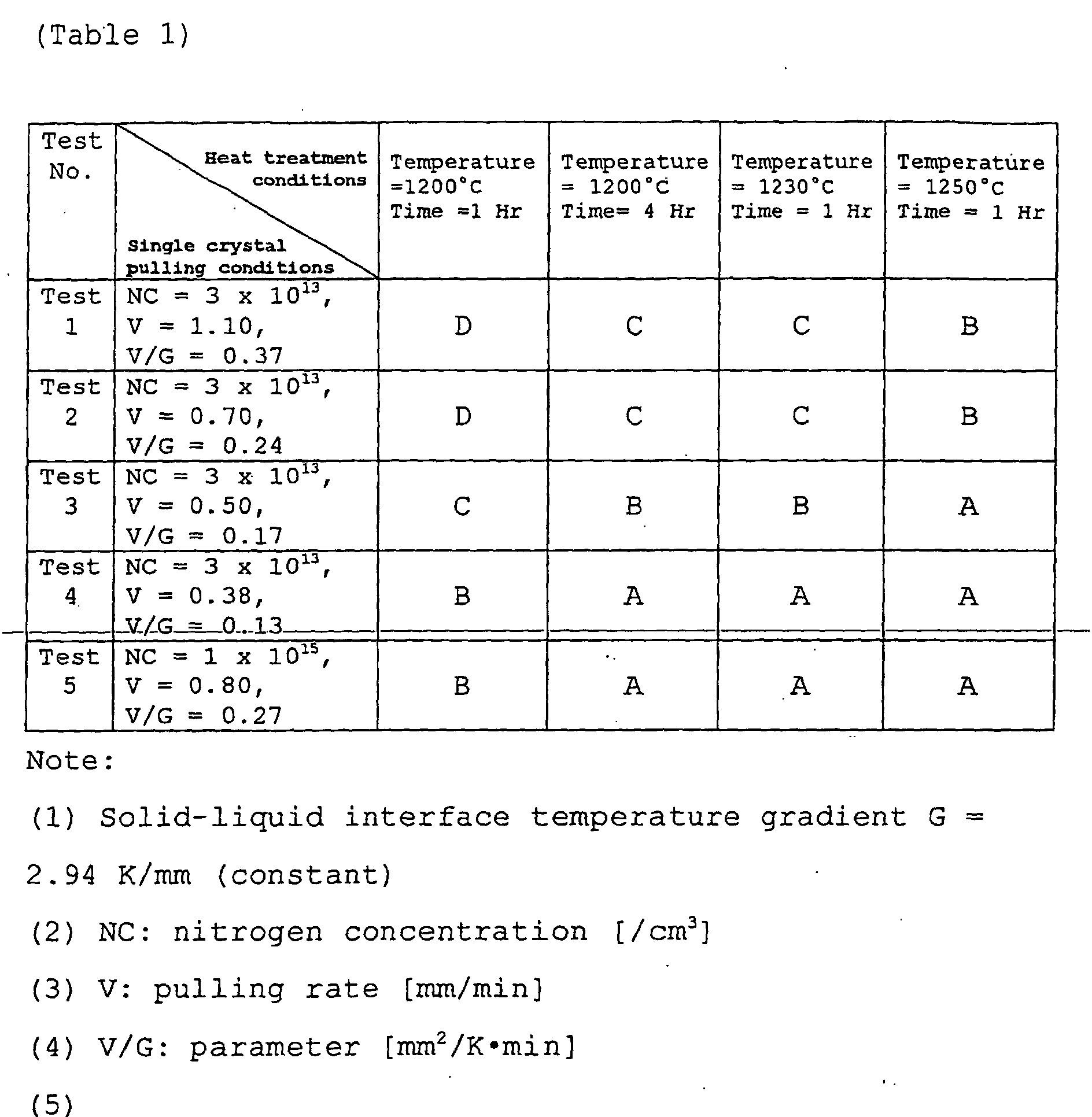
| Depth of COP free d (µm) | Notation |
| d < 1 | D |
| d ≒ 3 | C |
| 3 < d < 6 | B |
| d ≧ 6 | A |
Claims (5)
- A silicon single crystal wafer having a diameter of 300 mm or more and having a defect-free layer containing no COP for a depth of 3 microns or more from a surface.
- A method for producing a silicon single crystal, wherein, when a silicon single crystal having a diameter of 300 mm or more is pulled with nitrogen doping by the Czochralski method, the crystal is grown with a value of V/G [mm2/K•min] of 0.17 or less, where V [mm/min] is a pulling rate, and G [K/mm] is an average of temperature gradient in the crystal along a pulling axis from the melting point of silicon to 1400°C.
- A method for producing a silicon single crystal according to Claim 2, wherein the crystal is grown with a nitrogen concentration of 1 x 10¹³/cm3 or more for the nitrogen doping.
- A method for producing a silicon single crystal wafer in which a nitrogen-doped silicon single crystal wafer having a diameter of 300 mm or more is subjected to heat treatment, wherein the wafer is subjected to the heat treatment at 1230°C or more for 1 hour or more under an atmosphere of inert gas, hydrogen or a mixed gas thereof.
- A method for producing a silicon single crystal wafer, wherein a silicon single crystal wafer obtained by slicing a silicon single crystal produced by the method according to Claim 2 or 3 is subjected to the heat treatment defined in Claim 4.
Applications Claiming Priority (3)
| Application Number | Priority Date | Filing Date | Title |
|---|---|---|---|
| JP2001181587A JP2003002785A (en) | 2001-06-15 | 2001-06-15 | Silicon single crystal wafer having layer free from void defect at surface layer part and diameter of not less than 300 mm, and method for producing the same |
| JP2001181587 | 2001-06-15 | ||
| PCT/JP2002/005692 WO2002103091A1 (en) | 2001-06-15 | 2002-06-07 | SILICON SINGLE CRYSTAL WAFER HAVING VOID DENUDED ZONE ON THE SUFRACE AND DIAMETER OF AVOBE 300 mm AND ITS PRODUCTION METHOD |
Publications (2)
| Publication Number | Publication Date |
|---|---|
| EP1308544A1 true EP1308544A1 (en) | 2003-05-07 |
| EP1308544A4 EP1308544A4 (en) | 2009-02-11 |
Family
ID=19021829
Family Applications (1)
| Application Number | Title | Priority Date | Filing Date |
|---|---|---|---|
| EP02736029A Withdrawn EP1308544A4 (en) | 2001-06-15 | 2002-06-07 | SILICON SINGLE CRYSTAL WAFER HAVING VOID DENUDED ZONE ON THE SUFRACE AND DIAMETER OF ABOVE 300 mm AND ITS PRODUCTION METHOD |
Country Status (7)
| Country | Link |
|---|---|
| US (1) | US6902618B2 (en) |
| EP (1) | EP1308544A4 (en) |
| JP (1) | JP2003002785A (en) |
| KR (1) | KR20030036694A (en) |
| CN (1) | CN1463305A (en) |
| TW (1) | TWI265218B (en) |
| WO (1) | WO2002103091A1 (en) |
Families Citing this family (16)
| Publication number | Priority date | Publication date | Assignee | Title |
|---|---|---|---|---|
| JPWO2003003441A1 (en) * | 2001-06-28 | 2004-10-21 | 信越半導体株式会社 | Method of manufacturing annealed wafer and annealed wafer |
| JP2003059932A (en) * | 2001-08-08 | 2003-02-28 | Toshiba Ceramics Co Ltd | Method for manufacturing silicon single crystal wafer and silicon single crystal wafer |
| KR100588425B1 (en) * | 2003-03-27 | 2006-06-12 | 실트로닉 아게 | Method for the Production of a Silicon Single Crystal, Silicon Single Crystal and Silicon Semiconductor Wafers with determined Defect Distributions |
| JP4151474B2 (en) * | 2003-05-13 | 2008-09-17 | 信越半導体株式会社 | Method for producing single crystal and single crystal |
| KR100573473B1 (en) * | 2004-05-10 | 2006-04-24 | 주식회사 실트론 | Silicon Wafer and Manufacturing Method Thereof |
| US20060009011A1 (en) * | 2004-07-06 | 2006-01-12 | Gary Barrett | Method for recycling/reclaiming a monitor wafer |
| JP4806975B2 (en) * | 2005-06-20 | 2011-11-02 | 株式会社Sumco | Method for growing silicon single crystal |
| JP4710429B2 (en) * | 2005-06-20 | 2011-06-29 | 株式会社Sumco | Semiconductor single crystal manufacturing equipment |
| JP4821179B2 (en) * | 2005-06-20 | 2011-11-24 | 株式会社Sumco | Method for growing silicon single crystal |
| DE102007005346B4 (en) * | 2007-02-02 | 2015-09-17 | Siltronic Ag | Semiconductor wafers of silicon and process for their preparation |
| JP4359320B2 (en) * | 2007-05-31 | 2009-11-04 | Sumco Techxiv株式会社 | Doping apparatus and silicon single crystal manufacturing method |
| JP4516096B2 (en) * | 2007-05-31 | 2010-08-04 | Sumco Techxiv株式会社 | Method for producing silicon single crystal |
| EP2309038B1 (en) * | 2009-10-08 | 2013-01-02 | Siltronic AG | production method of an epitaxial wafer |
| DE102010007460B4 (en) * | 2010-02-10 | 2013-11-28 | Siltronic Ag | A method for pulling a single crystal of silicon from a melt contained in a crucible and thereby produced single crystal |
| CN101942701A (en) * | 2010-09-03 | 2011-01-12 | 浙江碧晶科技有限公司 | Heat treatment method of solar-grade silicon crystal |
| CN103911654B (en) * | 2014-04-15 | 2016-08-17 | 宁夏大学 | The method preparing the monocrystal silicon of a diameter of more than 400mm |
Family Cites Families (12)
| Publication number | Priority date | Publication date | Assignee | Title |
|---|---|---|---|---|
| JP3085146B2 (en) | 1995-05-31 | 2000-09-04 | 住友金属工業株式会社 | Silicon single crystal wafer and method of manufacturing the same |
| DE19637182A1 (en) * | 1996-09-12 | 1998-03-19 | Wacker Siltronic Halbleitermat | Process for the production of silicon wafers with low defect density |
| DE19983188T1 (en) * | 1998-05-01 | 2001-05-10 | Nippon Steel Corp | Silicon semiconductor substrate and method for its production |
| DE19823962A1 (en) * | 1998-05-28 | 1999-12-02 | Wacker Siltronic Halbleitermat | Method of manufacturing a single crystal |
| US6077343A (en) | 1998-06-04 | 2000-06-20 | Shin-Etsu Handotai Co., Ltd. | Silicon single crystal wafer having few defects wherein nitrogen is doped and a method for producing it |
| JP3943717B2 (en) | 1998-06-11 | 2007-07-11 | 信越半導体株式会社 | Silicon single crystal wafer and manufacturing method thereof |
| JP4233651B2 (en) * | 1998-10-29 | 2009-03-04 | 信越半導体株式会社 | Silicon single crystal wafer |
| JP4038910B2 (en) * | 1999-01-08 | 2008-01-30 | 株式会社Sumco | Manufacturing method of semiconductor silicon wafer |
| JP3734979B2 (en) * | 1999-03-23 | 2006-01-11 | シルトロニック・ジャパン株式会社 | Silicon semiconductor substrate and manufacturing method thereof |
| JP3870293B2 (en) | 1999-03-26 | 2007-01-17 | シルトロニック・ジャパン株式会社 | Silicon semiconductor substrate and manufacturing method thereof |
| JP3479001B2 (en) | 1999-08-27 | 2003-12-15 | コマツ電子金属株式会社 | Silicon wafer manufacturing method |
| US6599360B2 (en) | 2000-01-25 | 2003-07-29 | Shin-Etsu Handotai Co., Ltd. | Silicon wafer, method for determining production conditions of silicon single crystal and method for producing silicon wafer |
-
2001
- 2001-06-15 JP JP2001181587A patent/JP2003002785A/en active Pending
-
2002
- 2002-06-07 CN CN02802101A patent/CN1463305A/en active Pending
- 2002-06-07 US US10/344,423 patent/US6902618B2/en not_active Expired - Lifetime
- 2002-06-07 WO PCT/JP2002/005692 patent/WO2002103091A1/en not_active Ceased
- 2002-06-07 EP EP02736029A patent/EP1308544A4/en not_active Withdrawn
- 2002-06-07 KR KR10-2003-7002090A patent/KR20030036694A/en not_active Ceased
- 2002-06-12 TW TW091112809A patent/TWI265218B/en not_active IP Right Cessation
Also Published As
| Publication number | Publication date |
|---|---|
| US20030172865A1 (en) | 2003-09-18 |
| JP2003002785A (en) | 2003-01-08 |
| US6902618B2 (en) | 2005-06-07 |
| TWI265218B (en) | 2006-11-01 |
| WO2002103091A1 (en) | 2002-12-27 |
| KR20030036694A (en) | 2003-05-09 |
| EP1308544A4 (en) | 2009-02-11 |
| CN1463305A (en) | 2003-12-24 |
Similar Documents
| Publication | Publication Date | Title |
|---|---|---|
| EP1811065B1 (en) | Use of a single crystal silicon wafer for insulated gate bipolar transistors | |
| US7846252B2 (en) | Silicon wafer for IGBT and method for producing same | |
| US6191009B1 (en) | Method for producing silicon single crystal wafer and silicon single crystal wafer | |
| EP0959154B1 (en) | A method for producing an epitaxial silicon single crystal wafer and the epitaxial single crystal wafer | |
| TWI553173B (en) | An annealing wafer, an annealing wafer, and a method of manufacturing the device | |
| EP1326270B1 (en) | Method of manufacturing asilicon wafer and a silicon epitaxial wafer | |
| US6902618B2 (en) | Silicon single crystal wafer having void denuded zone on the surface and diameter of above 300 mm and its production method | |
| EP1170405A1 (en) | Silicon single crystal wafer and production method thereof and soi wafer | |
| US8231852B2 (en) | Silicon wafer and method for producing the same | |
| EP1326269A1 (en) | Method of producing silicon wafer and silicon wafer | |
| EP0942077B1 (en) | A method for producing a silicon single crystal wafer and a silicon single crystal wafer | |
| EP1195455B1 (en) | Method for determining condition under which silicon single crystal is produced, and method for producing silicon wafer | |
| EP1154048B1 (en) | Method of manufacture of a silicon epitaxial wafer | |
| JPWO2001055485A1 (en) | Method for determining manufacturing conditions for silicon wafers and silicon single crystals, and method for manufacturing silicon wafers | |
| EP1502972B1 (en) | A silicon single crystal wafer, an epitaxial wafer and method for producing silicon single crystal | |
| EP1536044B1 (en) | Method of manufacturing an epitaxial silicon wafer | |
| JP3614019B2 (en) | Manufacturing method of silicon single crystal wafer and silicon single crystal wafer | |
| US6273944B1 (en) | Silicon wafer for hydrogen heat treatment and method for manufacturing the same | |
| EP1343200A1 (en) | Anneal wafer manufacturing method and anneal wafer | |
| US6599603B1 (en) | Silicon wafer | |
| US6709957B2 (en) | Method of producing epitaxial wafers | |
| JPH11322491A (en) | Production of silicon single crystal wafer and silicon single crystal wafer | |
| KR100720659B1 (en) | Silicon wafer, its manufacturing method, evaluation method of silicon wafer | |
| EP1127962B1 (en) | Method for manufacturing silicon single crystal, silicon single crystal manufactured by the method, and silicon wafer | |
| JP2005072108A (en) | Manufacturing method of soi wafer and soi wafer |
Legal Events
| Date | Code | Title | Description |
|---|---|---|---|
| PUAI | Public reference made under article 153(3) epc to a published international application that has entered the european phase |
Free format text: ORIGINAL CODE: 0009012 |
|
| 17P | Request for examination filed |
Effective date: 20030225 |
|
| AK | Designated contracting states |
Designated state(s): AT BE CH CY DE DK ES FI FR GB GR IE IT LI LU MC NL PT SE TR |
|
| A4 | Supplementary search report drawn up and despatched |
Effective date: 20090114 |
|
| RIC1 | Information provided on ipc code assigned before grant |
Ipc: C30B 29/06 20060101AFI20030107BHEP Ipc: C30B 15/20 20060101ALI20090108BHEP Ipc: C30B 33/02 20060101ALI20090108BHEP |
|
| RAP1 | Party data changed (applicant data changed or rights of an application transferred) |
Owner name: SHIN-ETSU HANDOTAI CO., LTD. |
|
| STAA | Information on the status of an ep patent application or granted ep patent |
Free format text: STATUS: THE APPLICATION IS DEEMED TO BE WITHDRAWN |
|
| 18D | Application deemed to be withdrawn |
Effective date: 20090106 |