EP1307076A1 - Structure for interconnecting conductors and connecting method - Google Patents
Structure for interconnecting conductors and connecting method Download PDFInfo
- Publication number
- EP1307076A1 EP1307076A1 EP01949949A EP01949949A EP1307076A1 EP 1307076 A1 EP1307076 A1 EP 1307076A1 EP 01949949 A EP01949949 A EP 01949949A EP 01949949 A EP01949949 A EP 01949949A EP 1307076 A1 EP1307076 A1 EP 1307076A1
- Authority
- EP
- European Patent Office
- Prior art keywords
- layer
- solder
- conductor
- plating
- alloy
- Prior art date
- Legal status (The legal status is an assumption and is not a legal conclusion. Google has not performed a legal analysis and makes no representation as to the accuracy of the status listed.)
- Withdrawn
Links
Images


Classifications
-
- H—ELECTRICITY
- H05—ELECTRIC TECHNIQUES NOT OTHERWISE PROVIDED FOR
- H05K—PRINTED CIRCUITS; CASINGS OR CONSTRUCTIONAL DETAILS OF ELECTRIC APPARATUS; MANUFACTURE OF ASSEMBLAGES OF ELECTRICAL COMPONENTS
- H05K3/00—Apparatus or processes for manufacturing printed circuits
- H05K3/30—Assembling printed circuits with electric components, e.g. with resistors
- H05K3/32—Assembling printed circuits with electric components, e.g. with resistors electrically connecting electric components or wires to printed circuits
- H05K3/34—Assembling printed circuits with electric components, e.g. with resistors electrically connecting electric components or wires to printed circuits by soldering
-
- B—PERFORMING OPERATIONS; TRANSPORTING
- B23—MACHINE TOOLS; METAL-WORKING NOT OTHERWISE PROVIDED FOR
- B23K—SOLDERING OR UNSOLDERING; WELDING; CLADDING OR PLATING BY SOLDERING OR WELDING; CUTTING BY APPLYING HEAT LOCALLY, e.g. FLAME CUTTING; WORKING BY LASER BEAM
- B23K35/00—Rods, electrodes, materials, or media, for use in soldering, welding, or cutting
- B23K35/001—Interlayers, transition pieces for metallurgical bonding of workpieces
- B23K35/007—Interlayers, transition pieces for metallurgical bonding of workpieces at least one of the workpieces being of copper or another noble metal
-
- B—PERFORMING OPERATIONS; TRANSPORTING
- B23—MACHINE TOOLS; METAL-WORKING NOT OTHERWISE PROVIDED FOR
- B23K—SOLDERING OR UNSOLDERING; WELDING; CLADDING OR PLATING BY SOLDERING OR WELDING; CUTTING BY APPLYING HEAT LOCALLY, e.g. FLAME CUTTING; WORKING BY LASER BEAM
- B23K35/00—Rods, electrodes, materials, or media, for use in soldering, welding, or cutting
- B23K35/22—Rods, electrodes, materials, or media, for use in soldering, welding, or cutting characterised by the composition or nature of the material
- B23K35/24—Selection of soldering or welding materials proper
- B23K35/28—Selection of soldering or welding materials proper with the principal constituent melting at less than 950°C
- B23K35/282—Zn as the principal constituent
-
- H—ELECTRICITY
- H05—ELECTRIC TECHNIQUES NOT OTHERWISE PROVIDED FOR
- H05K—PRINTED CIRCUITS; CASINGS OR CONSTRUCTIONAL DETAILS OF ELECTRIC APPARATUS; MANUFACTURE OF ASSEMBLAGES OF ELECTRICAL COMPONENTS
- H05K3/00—Apparatus or processes for manufacturing printed circuits
- H05K3/30—Assembling printed circuits with electric components, e.g. with resistors
- H05K3/32—Assembling printed circuits with electric components, e.g. with resistors electrically connecting electric components or wires to printed circuits
- H05K3/34—Assembling printed circuits with electric components, e.g. with resistors electrically connecting electric components or wires to printed circuits by soldering
- H05K3/346—Solder materials or compositions specially adapted therefor
-
- B—PERFORMING OPERATIONS; TRANSPORTING
- B23—MACHINE TOOLS; METAL-WORKING NOT OTHERWISE PROVIDED FOR
- B23K—SOLDERING OR UNSOLDERING; WELDING; CLADDING OR PLATING BY SOLDERING OR WELDING; CUTTING BY APPLYING HEAT LOCALLY, e.g. FLAME CUTTING; WORKING BY LASER BEAM
- B23K35/00—Rods, electrodes, materials, or media, for use in soldering, welding, or cutting
- B23K35/22—Rods, electrodes, materials, or media, for use in soldering, welding, or cutting characterised by the composition or nature of the material
- B23K35/24—Selection of soldering or welding materials proper
- B23K35/26—Selection of soldering or welding materials proper with the principal constituent melting at less than 400°C
- B23K35/262—Sn as the principal constituent
-
- B—PERFORMING OPERATIONS; TRANSPORTING
- B23—MACHINE TOOLS; METAL-WORKING NOT OTHERWISE PROVIDED FOR
- B23K—SOLDERING OR UNSOLDERING; WELDING; CLADDING OR PLATING BY SOLDERING OR WELDING; CUTTING BY APPLYING HEAT LOCALLY, e.g. FLAME CUTTING; WORKING BY LASER BEAM
- B23K35/00—Rods, electrodes, materials, or media, for use in soldering, welding, or cutting
- B23K35/22—Rods, electrodes, materials, or media, for use in soldering, welding, or cutting characterised by the composition or nature of the material
- B23K35/24—Selection of soldering or welding materials proper
- B23K35/30—Selection of soldering or welding materials proper with the principal constituent melting at less than 1550°C
- B23K35/3013—Au as the principal constituent
-
- H—ELECTRICITY
- H05—ELECTRIC TECHNIQUES NOT OTHERWISE PROVIDED FOR
- H05K—PRINTED CIRCUITS; CASINGS OR CONSTRUCTIONAL DETAILS OF ELECTRIC APPARATUS; MANUFACTURE OF ASSEMBLAGES OF ELECTRICAL COMPONENTS
- H05K3/00—Apparatus or processes for manufacturing printed circuits
- H05K3/22—Secondary treatment of printed circuits
- H05K3/24—Reinforcing of the conductive pattern
- H05K3/244—Finish plating of conductors, especially of copper conductors, e.g. for pads or lands
-
- Y—GENERAL TAGGING OF NEW TECHNOLOGICAL DEVELOPMENTS; GENERAL TAGGING OF CROSS-SECTIONAL TECHNOLOGIES SPANNING OVER SEVERAL SECTIONS OF THE IPC; TECHNICAL SUBJECTS COVERED BY FORMER USPC CROSS-REFERENCE ART COLLECTIONS [XRACs] AND DIGESTS
- Y10—TECHNICAL SUBJECTS COVERED BY FORMER USPC
- Y10T—TECHNICAL SUBJECTS COVERED BY FORMER US CLASSIFICATION
- Y10T428/00—Stock material or miscellaneous articles
- Y10T428/12—All metal or with adjacent metals
- Y10T428/12493—Composite; i.e., plural, adjacent, spatially distinct metal components [e.g., layers, joint, etc.]
- Y10T428/12708—Sn-base component
-
- Y—GENERAL TAGGING OF NEW TECHNOLOGICAL DEVELOPMENTS; GENERAL TAGGING OF CROSS-SECTIONAL TECHNOLOGIES SPANNING OVER SEVERAL SECTIONS OF THE IPC; TECHNICAL SUBJECTS COVERED BY FORMER USPC CROSS-REFERENCE ART COLLECTIONS [XRACs] AND DIGESTS
- Y10—TECHNICAL SUBJECTS COVERED BY FORMER USPC
- Y10T—TECHNICAL SUBJECTS COVERED BY FORMER US CLASSIFICATION
- Y10T428/00—Stock material or miscellaneous articles
- Y10T428/12—All metal or with adjacent metals
- Y10T428/12493—Composite; i.e., plural, adjacent, spatially distinct metal components [e.g., layers, joint, etc.]
- Y10T428/12771—Transition metal-base component
- Y10T428/12785—Group IIB metal-base component
- Y10T428/12792—Zn-base component
-
- Y—GENERAL TAGGING OF NEW TECHNOLOGICAL DEVELOPMENTS; GENERAL TAGGING OF CROSS-SECTIONAL TECHNOLOGIES SPANNING OVER SEVERAL SECTIONS OF THE IPC; TECHNICAL SUBJECTS COVERED BY FORMER USPC CROSS-REFERENCE ART COLLECTIONS [XRACs] AND DIGESTS
- Y10—TECHNICAL SUBJECTS COVERED BY FORMER USPC
- Y10T—TECHNICAL SUBJECTS COVERED BY FORMER US CLASSIFICATION
- Y10T428/00—Stock material or miscellaneous articles
- Y10T428/12—All metal or with adjacent metals
- Y10T428/12493—Composite; i.e., plural, adjacent, spatially distinct metal components [e.g., layers, joint, etc.]
- Y10T428/12771—Transition metal-base component
- Y10T428/12861—Group VIII or IB metal-base component
- Y10T428/12882—Cu-base component alternative to Ag-, Au-, or Ni-base component
-
- Y—GENERAL TAGGING OF NEW TECHNOLOGICAL DEVELOPMENTS; GENERAL TAGGING OF CROSS-SECTIONAL TECHNOLOGIES SPANNING OVER SEVERAL SECTIONS OF THE IPC; TECHNICAL SUBJECTS COVERED BY FORMER USPC CROSS-REFERENCE ART COLLECTIONS [XRACs] AND DIGESTS
- Y10—TECHNICAL SUBJECTS COVERED BY FORMER USPC
- Y10T—TECHNICAL SUBJECTS COVERED BY FORMER US CLASSIFICATION
- Y10T428/00—Stock material or miscellaneous articles
- Y10T428/12—All metal or with adjacent metals
- Y10T428/12493—Composite; i.e., plural, adjacent, spatially distinct metal components [e.g., layers, joint, etc.]
- Y10T428/12771—Transition metal-base component
- Y10T428/12861—Group VIII or IB metal-base component
- Y10T428/12889—Au-base component
-
- Y—GENERAL TAGGING OF NEW TECHNOLOGICAL DEVELOPMENTS; GENERAL TAGGING OF CROSS-SECTIONAL TECHNOLOGIES SPANNING OVER SEVERAL SECTIONS OF THE IPC; TECHNICAL SUBJECTS COVERED BY FORMER USPC CROSS-REFERENCE ART COLLECTIONS [XRACs] AND DIGESTS
- Y10—TECHNICAL SUBJECTS COVERED BY FORMER USPC
- Y10T—TECHNICAL SUBJECTS COVERED BY FORMER US CLASSIFICATION
- Y10T428/00—Stock material or miscellaneous articles
- Y10T428/12—All metal or with adjacent metals
- Y10T428/12493—Composite; i.e., plural, adjacent, spatially distinct metal components [e.g., layers, joint, etc.]
- Y10T428/12771—Transition metal-base component
- Y10T428/12861—Group VIII or IB metal-base component
- Y10T428/12903—Cu-base component
-
- Y—GENERAL TAGGING OF NEW TECHNOLOGICAL DEVELOPMENTS; GENERAL TAGGING OF CROSS-SECTIONAL TECHNOLOGIES SPANNING OVER SEVERAL SECTIONS OF THE IPC; TECHNICAL SUBJECTS COVERED BY FORMER USPC CROSS-REFERENCE ART COLLECTIONS [XRACs] AND DIGESTS
- Y10—TECHNICAL SUBJECTS COVERED BY FORMER USPC
- Y10T—TECHNICAL SUBJECTS COVERED BY FORMER US CLASSIFICATION
- Y10T428/00—Stock material or miscellaneous articles
- Y10T428/24—Structurally defined web or sheet [e.g., overall dimension, etc.]
- Y10T428/24942—Structurally defined web or sheet [e.g., overall dimension, etc.] including components having same physical characteristic in differing degree
- Y10T428/2495—Thickness [relative or absolute]
-
- Y—GENERAL TAGGING OF NEW TECHNOLOGICAL DEVELOPMENTS; GENERAL TAGGING OF CROSS-SECTIONAL TECHNOLOGIES SPANNING OVER SEVERAL SECTIONS OF THE IPC; TECHNICAL SUBJECTS COVERED BY FORMER USPC CROSS-REFERENCE ART COLLECTIONS [XRACs] AND DIGESTS
- Y10—TECHNICAL SUBJECTS COVERED BY FORMER USPC
- Y10T—TECHNICAL SUBJECTS COVERED BY FORMER US CLASSIFICATION
- Y10T428/00—Stock material or miscellaneous articles
- Y10T428/26—Web or sheet containing structurally defined element or component, the element or component having a specified physical dimension
- Y10T428/263—Coating layer not in excess of 5 mils thick or equivalent
- Y10T428/264—Up to 3 mils
- Y10T428/265—1 mil or less
Definitions
- the present invention relates to a technique for connecting a conductor having a surface formed with an Au layer with another conductor via a solder.
- a terminal of the electronic component is electrically and mechanically connected to a terminal pad provided on the circuit board via a solder.
- a terminal pad of a circuit board may be provided, for example, by forming a Cu wiring pattern on the circuit board and then laminating an Ni-plating layer and an Au-plating layer at a portion to become the terminal pad.
- the Au-plating layer is provided as the uppermost layer to prevent the surface of the terminal pad from oxidizing to provide a reliable connection with the terminal of the electronic component.
- the Ni-plating is provided because it is difficult to directly provide the Au-plating on the Cu wiring pattern and because Ni itself is likely to oxidize at the surface thereof.
- solder a 63Sn-37Pb solder is generally used. Recently, however, by environmental regulations such as the Waste Disposal Act, Pb is designated as a substance for special control, and the influence of Pb on the environment is concerned about. For this reason, the conventionally used solder is being replaced with a solder which does not contain Pb (Pb-free solder).
- an Sn-Ag solder As a promising Pb-free solder, attention is focused on an Sn-Ag solder, and an Sn-Ab based solder which further contains Cu or Bi.
- an electronic component When an electronic component is connected to a circuit board having the above-described structure using such an Sn-Ag based solder, the Sn atoms in the solder layer diffuse into the Ni-plating layer to form an Sn-Ni alloy layer. Through the alloy layer and the solder layer, the terminal of the circuit board is connected to the terminal of the electronic component.
- the Au-plating layer formed on the surface of the Ni-plating layer breaks, diffusing Au into the solder layer. Since Au and Sn are highly reactive with each other, these elements are bonded to form an intermetallic compound.
- the Au-Sn intermetallic compound deteriorates the mechanical strength of the solder layer. For example, it is said that the connection strength largely deteriorates when the concentration of the Au-Sn intermetallic compound in the entire solder layer becomes about 5wt% or when the Au-Sn intermetallic compound is locally formed to have a local concentration of about 5wt%. Therefore, there exists even a report which concludes that another conductor cannot be connected to an Au-plating layer using a solder.
- the thickness of the Au-plating layer is relatively large, so that a relatively large amount of Au diffuses in the solder layer.
- the concentration of the Au-Sn intermetallic compound in the solder layer is high, so that the problem as to the connection strength is more serious.
- solder bonding may be performed in an inert atmosphere by feeding an inert gas, which is, however, disadvantageous in terms of cost.
- an additional terminal pad for direct contact with a terminal of a battery or a terminal of a charger need be formed besides the terminal pad for mounting an electronic component (mounting terminal pad). Since such an additional terminal pad is to be exposed in the air for a long period of time, the surface thereof is usually plated with gold for preventing the oxidization. Therefore, to provide a mounting terminal pad which is not provided with Au-plating, the mounting terminal pad need be covered with a mask and the mask need be removed after the completion of the plating. Such process steps deteriorate the manufacturing efficiency while increasing the cost.
- the mounting terminal pad need be selectively formed with a mask, which deteriorates the manufacturing efficiency more largely. Therefore, in view of the cost, in a circuit board for use as a protective circuit or the like, it is expedient to apply Au-plating simultaneously to the mounting terminal pad and to the additional terminal pad.
- An object of the present invention which is conceived under the circumstances described above, is to provide a technique for connecting a conductor having a surface formed with an Au layer with another conductor via a solder in a cost-effective manner and with a high connection reliability.
- connection structure comprising a first conductor having a surface formed with an Au layer, a second conductor which is conductive at least at a surface thereof, and a solder for connecting the first conductor to the second conductor, the first conductor being connected to the second conductor via an Au-Zn alloy layer.
- the first conductor includes a conductor layer having an obverse surface formed with an Au-plating layer, and the Au-Zn alloy layer joins the conductor layer to a layer of the solder formed at the second conductor.
- the Au-Zn alloy layer may have a thickness of 0.1 ⁇ 10 ⁇ m, for example.
- the solder layer comprises an Sn-Zn alloy layer. It is particularly preferable that the Sn-Zn alloy layer contains Sn and Zn generally at a eutectic alloy ratio, because such an alloy has a low melting point.
- the Sn-Zn alloy layer may further contain Bi.
- the first conductor may comprise a Cu layer, an Ni layer and an Au layer which are successively laminated.
- a method for connecting a first conductor having a surface formed with an Au layer to a second conductor which is conductive at least at a surface thereof via solder includes the steps of interposing a solder containing Zn between the first conductor and the second conductor, melting the solder, and then solidifying the solder.
- the solder may be an Sn-Zn eutectic solder.
- the Sn-Zn eutectic solder may further contain Bi.
- the Au layer has a thickness of 0.1 ⁇ 10 ⁇ m, for example.
- the Au layer may be formed by electrolytic plating, for example .
- the first conductor may comprise a Cu layer, an Ni layer and an Au layer which are successively laminated.
- the first conductor may be a terminal pad of a circuit board, whereas the second conductor may be a terminal of an electronic component or a conductor plate.
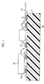
- Fig. 1 is a sectional view illustrating a connection structure of conductors according to an embodiment of the present invention.
- a circuit board 1 includes a protective circuit for preventing the overcharge of a rechargeable battery for example.
- the circuit board 1 comprises a substrate 10 formed of, for example, glass-fiber-reinforced epoxy resin, and a wiring pattern (not shown) of Cu formed on the substrate.
- the Cu wiring pattern may be provided by forming a Cu film having a thickness of about 15 ⁇ 25 ⁇ m entirely on a surface of the substrate 10 by CVD or vapor deposition for example and then removing unnecessary portions by etching.
- the Cu wiring pattern is provided, at appropriate portions thereof, with a plurality of terminal pads 11a, 11b, 11c to which terminals 20a, 21a of electronic components 20, 21 and a terminal plate 22 are connected.
- Each of the terminal pads 11a, 11b and 11c may be made by forming an Ni-plating layer at a pad-forming portion on the Cu-wiring pattern and then forming an Au-plating layer thereon.
- the Ni-plating layer may be formed, for example, by electrolytic plating to a thickness of about 10 ⁇ m.
- the Au-plating layer may be formed, for example, by electrolytic plating or electroless plating to a thickness of 0.1 ⁇ 10 ⁇ m, and more preferably, to a thickness of 0.5 ⁇ 5 ⁇ m.
- the electronic components 20, 21 and the terminal plate 22 are mounted utilizing solders H.
- the electronic component 20 is a bear chip
- the electronic component 21 is a semiconductor device 21 of a resin-packaged type.
- the terminal plate 22 may be made of nickel for example.
- the kind of components to be mounted to the circuit board 1 is not limitative.
- a semiconductor device of a pin insertion type or a chip resistor may be mounted to the circuit board 1.
- the mounting to the circuit board 1 may be performed as follows.
- solder paste is printed on the terminal pads 11a, 11b, 11c of the circuit board 1, the terminals 20a, 21a of the electronic components 20, 21 and a predetermined portion of the terminal plate 22 in advance. Alternatively, solder plating may be applied to these portions.
- the solder to be used in this embodiment is not limited as long as it contains Zn.
- use may be made of a solder containing Zn only, or of a solder containing selected one or ones of Pb, Sn, Cu and Bi in addition to Zn.
- an Sn-Zn eutectic solder may suitably be used in view of its Pb-free feature and low melting point.
- the Sn-Zn eutectic solder means a solder containing Sn and Zn at the ratio which makes the solder eutectic or at a ratio close to that ratio.
- the solder may further contain Bi or Cu as the third component.
- each of the electronic components 20, 21 and the terminal plate 22 is electrically and mechanically connected to the circuit board 1.
- the circuit board 1 at appropriate positions of which the electronic components 20 and the like are disposed is put into a reflow furnace heated to a temperature equal to or higher than the melting point of the solder for re-melting the solders H.
- the circuit board 1 is taken out from the reflow furnace and the solders H are cooled for solidification. In this way, each of the electronic components 20, 21 and the terminal plate 22 is mounted to the circuit board 1.
- the melting point of the Sn-Zn eutectic solder is about 199°C. Therefore, when the Sn-Zn eutectic solder is used, a temperature of about 240°C, for example, is sufficient as the temperature of the reflow furnace. Such a temperature is generally equal to the temperature of a reflow furnace conventionally used for reflow soldering using Sn-Pb solder for providing electric connection. Such a temperature is also sufficiently low so that the electronic components are not damaged by heat.
- the electronic components 20, 21 and the terminal plate 22 or the like can be mounted and connected to the circuit board 1 by reflow soldering using the existing equipment (i.e., without preparing new equipment) and without causing much thermal damage to the electronic components.
- the electronic components 20, 21 and the terminal plate 22 are connected to the terminal pads 11a, 11b, 11c each including an Au-plating layer via the solders H containing Sn. Therefore, from the conventional common knowledge, one may afraid that, similarly to the case where an Sn-Ag based solder is used, Au atoms may diffuse in the solder H to form an Au-Sn intermetallic compound, resulting in a decrease in the connection strength.
- the inventor of the present invention has found that the connection structure provided by using the Sn-Zn eutectic solder has sufficient mechanical stability.
- One sample I included a Cu wiring pattern (having a thickness of about 20 ⁇ m) formed on a substrate made of glass-fiber-reinforced epoxy resin.
- the Cu wiring pattern was formed with a terminal pad comprising an Ni-plating layer (having a thickness of about 10 ⁇ m) and an Au-plating layer (having a thickness of about 0.8 ⁇ m).
- the two kinds of samples were the same with respect to the conditions other than the kind of a solder, the condition of the applying of the solder, the structure of a terminal pad of the circuit board. (For example, they were the same with respect to the reflowing temperature and the shape of the terminal plate).
- each of the samples I was found to have a connection strength which is generally equal to or higher than that in each of the samples II. From this result, the inventor of the present invention surmised that the Zn component contained in the Sn-Zn eutectic solder functioned to prevent Au atoms of the Au-plating layer from diffusing in the solder layer.
- the inventor analyzed the sectional structure and composition between a circuit board and a terminal pad with respect to the case where the connection between the terminal plate and the circuit board was made using a solder containing Zn and the case where such connection was made using a solder which did not contain Zn.
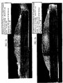
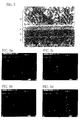
- connection section the section at the terminal pad (hereinafter referred to as "connection section") was polished, and the connection section was checked using an optical microscope (Tradename: SZ-60, Supplier: Olympus Optical Co., Ltd.). Figs.
- FIG. 2a and 2b show the conditions of connection sections as magnified 50 times.
- Fig. 2a shows the condition of the connection section when Sn-8Zn-3Bi solder is used
- objects like a Cu-wiring pattern and a solder layer were seen on the substrate in each figure, no clear difference of the condition of the connection section was found between the case where the solder containing Zn was used (Fig. 2a) and the case where the solder which did not contain Zn was used (Fig. 2b).
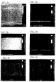
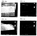
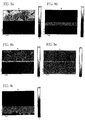
- Figs. 3a ⁇ 3f are mappings showing concentration profiles at the connection section when Sn-3.0Ag-0.5Cu solder is used, whereas Figs. 4a ⁇ 4f are mappings showing concentration profiles at the connection section when Sn-8Zn-3Bi solder is used.
- the EPMA was performed using "EPMA 8705" of Shimadzu Corporation.
- Fig. 3a is a monochromatic mapping photograph of the concentration profile of all the components when the connection is made using Sn-3.0Ag-0.5Cu solder. This photograph shows the distribution region of each of the components.
- Figs. 3b ⁇ 3d are color mapping photographs of respective concentration profiles of Sn elements, Ag elements and Cu elements constituting the Sn-3.0Ag-0.5Cu solder. From the comparison of these figures with Fig. 3a, it is confirmed that the solder layer consists of Sn elements, Ag elements and Cu elements. Since Cu elements are the component constituting the Cu wiring pattern, the region where the Cu concentration is high is found on the substrate. Further, it is also confirmed that part of Sn leaves the solder layer to diffuse in the Cu wiring pattern.
- Fig. 3e shows the concentration profile of Ni elements. From the comparison of this figure with Fig. 3a, it is found that most of the Ni elements remain on the Cu wiring pattern, while some of the Ni elements have diffused into the solder layer. Since the region where the Ni concentration is high generally coincides with the region to which the Sn elements from the solder layer is distributed, it is surmised that Sn has diffused into the Ni plating layer to form an Sn-Ni alloy layer on the Cu wiring pattern.
- Fig. 3f shows the concentration profile of Au elements. From the comparison of this figure with Fig. 3a, it is confirmed that Au has diffused in the solder layer. Since a band-like region of a high Au concentration is not seen, it is considered that the Au-plating layer has broken.
- Fig. 4a is a monochromatic mapping photograph of the concentration profile of all the components when the connection is made using Sn-8Zn-3Bi solder. This photograph shows the distribution region of each of the components.
- Figs. 4b ⁇ 4d are color mapping photographs of respective concentration profiles of Sn elements, Zn elements and Bi elements constituting the Sn-8Zn-3Bi solder. From the comparison of these figures with Fig. 4a, it is confirmed that the solder layer consists of Sn elements, Zn elements and Bi elements and that a region where the Zn concentration is high is formed at a lower region of the solder layer or separately from the solder layer.
- Fig. 4e shows the concentration profile of Cu elements. From the comparison of this figure with Fig. 4a, it is surmised that most of Cu elements remain on the substrate to form the Cu wiring pattern while some of the Cu elements have diffused in the solder layer.
- Fig. 4f shows the concentration profile of Ni elements. From the comparison of this figure with Figs. 4a and 4e, it is surmised that most of the Ni elements remain on the Cu wiring pattern to form the Ni-plating layer while some of the Ni elements have diffused in the solder layer.
- Fig. 4g shows the concentration profile of Au elements. From the comparison of this figure with Figs. 4a and 4f, it is surmised that Au has hardly diffused in the solder layer and most of the Au elements remain on the Ni plating layer.
- connection section and the composition with respect to the case where an Sn-8Zn-3Bi solder is used.
- connection section consists of four layers , i.e. layers a ⁇ d.
- the connection section consists of four layers , i.e. layers a ⁇ d.
- three of these layers are presumably a Cu wiring pattern, an Ni-plating layer and a solder layer, respectively. Therefore, since the remaining layer is only one, it is considered that Zn does not solely form a layer but Zn together with Au form the one layer.
- composition analysis was performed for each of the layers a ⁇ d by electron diffraction (ED) analysis.
- the electron diffraction was performed using "EMAX2770" manufactured by Horiba, Ltd.
- Figs. 6a ⁇ 6d each is a color chart photograph showing the result of the composition analysis of each layer. It is to be noted that, although tungsten appears as a peak W in each color chart photograph, this is not a component constituting each layer but just appears because it is used for coating the surface of a connection section in analysis.
- Fig. 6a is a chart showing the result of the composition analysis of the layer a. From the fact that most of the detected structural elements of the layer a are Cu, the layer a is concluded to be a Cu wiring pattern as surmised.
- Fig. 6b is a chart showing the result of the composition analysis of the layer b. Much Ni is detected as a structural element of the layer b, though C is also detected. From this result, the layer b is concluded to be an Ni-plating layer as surmised.
- Fig. 6c is a chart showing the result of the composition analysis of the layer c.
- the layer c is not a Zn layer solely composed of Zn but an Au-Zn alloy layer formed on the Ni-plating layer. It is probable that the Zn elements in the layer c have come from the solder material. Therefore, it is considered that the Au-Zn alloy layer has formed based on the Au-plating layer as a result of the diffusion of Zn into the Au-plating layer during the solder reflowing process while preventing the diffusion of Au toward the solder layer.
- Fig. 6d is a chart showing the result of the composition analysis of the layer d.
- Sn and Zn are detected.
- the layer d is concluded to be a solder layer consisted of Sn, Zn and Bi.
- Au is hardly detected in the layer d, which means that Au constituting the Au-plating layer has hardly diffused in the solder layer.
- the reasons why Bi does not appear in Fig. 6d as a recognizably high peak is that the content of Bi in the solder material is 3wt (one twentieth of Sn) at the most and that the measurement range is set based on Sn.
- each layer a ⁇ d is generally determined from the results of the electron diffraction analysis. This analysis is particularly meaningful in that the layer c is generally concluded to be an Au-Zn alloy layer and that Au has not been detected in the layer d (solder layer).
- the inventor analyzed the concentration profile of each component at the connection section by Auger electron spectroscopy (AES) analysis, which is a more precise analyzing method.
- AES Auger electron spectroscopy
- connection section to be subjected to the Auger electron spectroscopy analysis is checked using an SEM (scanning electron microscope).
- Fig. 7 shows the SEM photograph, which confirms that the connection section includes four layers (layers a ⁇ d) which are supposed to be a Cu wiring pattern, an Ni-plating layer, an Au-Zn alloy layer and an Sn-Zn-Bi solder layer, respectively.
- Fig. 8a is a mapping photograph showing the measurements of the concentration profile of Sn. From this photograph, it is found that Sn is distributed to the region corresponding to the layer d. This result coincides with the results of the EPMA and the electron diffraction analysis.
- Fig. 8b is a mapping photograph showing the measurements of the concentration profile of Zn. From this photograph, it is found that Zn is distributed to the region corresponding to the layer d and that a region of a high Zn concentration exists in the layer c. This result also coincides with the results of the EPMA and the electron diffraction analysis. By considering this result together with Fig. 8a, the layer d is concluded to be an Sn-Zn alloy layer. From the result of the EPMA, it is clear that Bi is diffused in the layer d. Therefore, there is no doubt that the layer d is an Sn-Zn-Bi solder layer.
- Fig. 8c is a mapping photograph showing the measurements of the concentration profile of Cu. From this photograph, it is found that Cu is distributed to the region corresponding to the layer a. This result coincides with the results of the EPMA and the electron diffraction analysis. Therefore, there is no doubt that the layer a is a Cu wiring pattern.
- Fig. 8d is a mapping photograph showing the measurements of the concentration profile of Ni. From this photograph, it is found that Ni is distributed to the region corresponding to the layer b. This result coincides with the results of the EPMA and the electron diffraction analysis. Therefore, there is no doubt that the layer b is an Ni-plating layer.
- Fig. 8e is a mapping photograph showing the measurements of the concentration profile of Au. From this photograph, it is found that Au is distributed to the region corresponding to the layer c. Since Au is an element which is difficult to measure, the measurement is performed with an increased sensitivity. Therefore, the photograph shows entirely whitish as if Au is distributed to the entire region. In fact, however, Au is distributed to the layer c only. By considering this result together with Fig. 8b, there is no doubt that the layer c is an Au-Zn alloy layer. From the fact that an Au-plating layer is originally formed on an Ni-plating layer, it is concluded that the Au-Zn alloy layer is formed as a result of the diffusion of Zn, which is a component of the solder, into the Au plating layer.
- the layer c i.e. the Au-Zn alloy layer is found to have a thickness of about 2 ⁇ 3 ⁇ m, although the Au plating layer originally had a thickness of about 0.8 ⁇ m. Therefore, it is surmised that the ratio of Au to Zn in the Au-Zn alloy layer is about 1:1 ⁇ 3.
- connection structure between the substrate and the terminal plate comprises a Cu wiring pattern, an Ni-plating layer, an Au-Zn alloy layer and an Sn-Zn-Bi solder layer.
- the Au-Zn alloy layer is interposed between the Ni-plating layer and the solder layer.
- the Au-Zn alloy layer functions to bond the solder to the terminal pad. Since Ni is compatible with Au, the Au-Zn alloy layer is reliably bonded to the Ni-plating layer. Further, since Au and Sn have a good affinity with each other and both the Au-Zn alloy layer and the solder layer contain Zn, reliable bonding is provided also between the Au-Zn alloy layer and the solder layer.
- connection structure wherein an Au-Zn alloy layer is interposed between the Ni-plating layer and the Sn-Zn solder layer, high mechanical strength is obtained. As described before, this fact is confirmed also from the measurements in the tearing-off test performed for measuring the connection strength between a terminal plate and a circuit board.
- Au is hardly diffused in the solder layer. This is because the diffusion of Au is prevented by the Au-Zn alloy layer which is formed as a result of the diffusion of Zn into the Au-plating layer. That is, Zn has a function to prevent Au constituting the Au-plating layer from diffusing into the solder layer.
- the prevention of the Au diffusion leads to the prevention of the generation of an Au-Sn intermetallic compound in the solder layer.
- a conductor e.g. a terminal pad
Landscapes
- Engineering & Computer Science (AREA)
- Mechanical Engineering (AREA)
- Manufacturing & Machinery (AREA)
- Microelectronics & Electronic Packaging (AREA)
- Electric Connection Of Electric Components To Printed Circuits (AREA)
- Parts Printed On Printed Circuit Boards (AREA)
- Manufacturing Of Printed Wiring (AREA)
- Production Of Multi-Layered Print Wiring Board (AREA)
Abstract
A first conductor having a surface formed with an Au layer
is connected, via a Zn-containing solder, to a second conductor
which is conductive at least at a surface thereof. The first
conductor may be, for example, a terminal pad (11a, 11b, 11c)
constituting a part of a wiring pattern on a circuit board (1),
whereas the second conductor may be a terminal (20a, 21a) of
an electronic component (20, 21) or a terminal plate (22). The
first conductor is connected to the second conductor via an
Au-Zn alloy layer which is formed as a result of the diffusion
of Zn from the Zn-containing solder into the Au layer of the
first conductor.
Description
The present invention relates to a technique for
connecting a conductor having a surface formed with an Au layer
with another conductor via a solder.
Conventionally, as a method for mounting an electronic
component such as a semiconductor chip to a circuit board for
example, a terminal of the electronic component is electrically
and mechanically connected to a terminal pad provided on the
circuit board via a solder. Such a terminal pad of a circuit
board may be provided, for example, by forming a Cu wiring
pattern on the circuit board and then laminating an Ni-plating
layer and an Au-plating layer at a portion to become the terminal
pad. The Au-plating layer is provided as the uppermost layer
to prevent the surface of the terminal pad from oxidizing to
provide a reliable connection with the terminal of the
electronic component. The Ni-plating is provided because it
is difficult to directly provide the Au-plating on the Cu wiring
pattern and because Ni itself is likely to oxidize at the surface
thereof.
Conventionally, for the solder, a 63Sn-37Pb solder is
generally used. Recently, however, by environmental
regulations such as the Waste Disposal Act, Pb is designated
as a substance for special control, and the influence of Pb
on the environment is worried about. For this reason, the
conventionally used solder is being replaced with a solder
which does not contain Pb (Pb-free solder).
As a promising Pb-free solder, attention is focused on
an Sn-Ag solder, and an Sn-Ab based solder which further
contains Cu or Bi. When an electronic component is connected
to a circuit board having the above-described structure using
such an Sn-Ag based solder, the Sn atoms in the solder layer
diffuse into the Ni-plating layer to form an Sn-Ni alloy layer.
Through the alloy layer and the solder layer, the terminal of
the circuit board is connected to the terminal of the electronic
component.
In this case, the Au-plating layer formed on the surface
of the Ni-plating layer breaks, diffusing Au into the solder
layer. Since Au and Sn are highly reactive with each other,
these elements are bonded to form an intermetallic compound.
The Au-Sn intermetallic compound deteriorates the mechanical
strength of the solder layer. For example, it is said that
the connection strength largely deteriorates when the
concentration of the Au-Sn intermetallic compound in the entire
solder layer becomes about 5wt% or when the Au-Sn intermetallic
compound is locally formed to have a local concentration of
about 5wt%. Therefore, there exists even a report which
concludes that another conductor cannot be connected to an
Au-plating layer using a solder. Particularly, when an
Au-plating layer is formed by electrolytic plating, the
thickness of the Au-plating layer is relatively large, so that
a relatively large amount of Au diffuses in the solder layer.
In such a case, the concentration of the Au-Sn intermetallic
compound in the solder layer is high, so that the problem as
to the connection strength is more serious.
Therefore, an attempt is also made to connect a terminal
pad of a circuit board to a terminal of an electronic component
via a solder without forming an Au-plating layer on the terminal
pad (or, in some cases, even without forming an Ni-plating
layer). However, the surface of such a terminal pad at which
the Ni-plating layer or the Cu wiring is exposed is likely to
oxidize due to the heat in soldering, which deteriorates the
connection reliability of the electronic component. To solve
these problems, solder bonding may be performed in an inert
atmosphere by feeding an inert gas, which is, however,
disadvantageous in terms of cost.
Moreover, in a circuit board for use as a protective
circuit of a rechargeable battery of a mobile phone for example,
an additional terminal pad for direct contact with a terminal
of a battery or a terminal of a charger need be formed besides
the terminal pad for mounting an electronic component (mounting
terminal pad). Since such an additional terminal pad is to
be exposed in the air for a long period of time, the surface
thereof is usually plated with gold for preventing the
oxidization. Therefore, to provide a mounting terminal pad
which is not provided with Au-plating, the mounting terminal
pad need be covered with a mask and the mask need be removed
after the completion of the plating. Such process steps
deteriorate the manufacturing efficiency while increasing the
cost. Particularly when the Au-plating is provided by
electrolytic plating, the mounting terminal pad need be
selectively formed with a mask, which deteriorates the
manufacturing efficiency more largely. Therefore, in view of
the cost, in a circuit board for use as a protective circuit
or the like, it is expedient to apply Au-plating simultaneously
to the mounting terminal pad and to the additional terminal
pad.
An object of the present invention, which is conceived
under the circumstances described above, is to provide a
technique for connecting a conductor having a surface formed
with an Au layer with another conductor via a solder in a
cost-effective manner and with a high connection reliability.
According to a first aspect of the present invention,
there is provided a connection structure comprising a first
conductor having a surface formed with an Au layer, a second
conductor which is conductive at least at a surface thereof,
and a solder for connecting the first conductor to the second
conductor, the first conductor being connected to the second
conductor via an Au-Zn alloy layer.
Preferably, the first conductor includes a conductor
layer having an obverse surface formed with an Au-plating layer,
and the Au-Zn alloy layer joins the conductor layer to a layer
of the solder formed at the second conductor. The Au-Zn alloy
layer may have a thickness of 0.1∼10µm, for example.
Preferably, the solder layer comprises an Sn-Zn alloy
layer. It is particularly preferable that the Sn-Zn alloy
layer contains Sn and Zn generally at a eutectic alloy ratio,
because such an alloy has a low melting point.
The Sn-Zn alloy layer may further contain Bi. In such
a case, the Sn-Zn-Bi alloy layer may have a composition of
Sn:Zn:Bi=85∼95:8∼12:1∼10, for example.
In a preferred embodiment, the first conductor may
comprise a Cu layer, an Ni layer and an Au layer which are
successively laminated.
According to a second aspect of the present invention,
there is provided a method for connecting a first conductor
having a surface formed with an Au layer to a second conductor
which is conductive at least at a surface thereof via solder.
The method includes the steps of interposing a solder
containing Zn between the first conductor and the second
conductor, melting the solder, and then solidifying the solder.
Preferably, the solder may be an Sn-Zn eutectic solder.
The Sn-Zn eutectic solder may further contain Bi. In such a
case, the solder has a composition of
Sn:Zn:Bi=85∼95:8∼12:1∼10.
The Au layer has a thickness of 0.1∼10µm, for example.
The Au layer may be formed by electrolytic plating, for example .
In a preferred embodiment, the first conductor may
comprise a Cu layer, an Ni layer and an Au layer which are
successively laminated. The first conductor may be a terminal
pad of a circuit board, whereas the second conductor may be
a terminal of an electronic component or a conductor plate.
Other features and advantages of the present invention
will become clearer from the description of the embodiments
given below with reference to the accompanying drawings.
Other features and advantages of the present invention
will become clearer from the description given below with
reference to the accompanying drawings.
A preferred embodiment of the present invention will be
described below in detail with reference to Fig. 1. Fig. 1
is a sectional view illustrating a connection structure of
conductors according to an embodiment of the present invention.
In Fig. 1, a circuit board 1 includes a protective circuit
for preventing the overcharge of a rechargeable battery for
example. The circuit board 1 comprises a substrate 10 formed
of, for example, glass-fiber-reinforced epoxy resin, and a
wiring pattern (not shown) of Cu formed on the substrate. The
Cu wiring pattern may be provided by forming a Cu film having
a thickness of about 15∼25µm entirely on a surface of the
substrate 10 by CVD or vapor deposition for example and then
removing unnecessary portions by etching.
The Cu wiring pattern is provided, at appropriate portions
thereof, with a plurality of terminal pads 11a, 11b, 11c to
which terminals 20a, 21a of electronic components 20, 21 and
a terminal plate 22 are connected. Each of the terminal pads
11a, 11b and 11c may be made by forming an Ni-plating layer
at a pad-forming portion on the Cu-wiring pattern and then
forming an Au-plating layer thereon. The Ni-plating layer may
be formed, for example, by electrolytic plating to a thickness
of about 10µm. The Au-plating layer may be formed, for example,
by electrolytic plating or electroless plating to a thickness
of 0.1∼10µm, and more preferably, to a thickness of 0.5∼5µm.
To the circuit board 1 having such a structure, the
electronic components 20, 21 and the terminal plate 22 are
mounted utilizing solders H. In the illustrated embodiment,
the electronic component 20 is a bear chip, whereas the
electronic component 21 is a semiconductor device 21 of a
resin-packaged type. The terminal plate 22 may be made of
nickel for example. The kind of components to be mounted to
the circuit board 1 is not limitative. For example, a
semiconductor device of a pin insertion type or a chip resistor
may be mounted to the circuit board 1. The mounting to the
circuit board 1 may be performed as follows.
First, solder paste is printed on the terminal pads 11a,
11b, 11c of the circuit board 1, the terminals 20a, 21a of the
electronic components 20, 21 and a predetermined portion of
the terminal plate 22 in advance. Alternatively, solder
plating may be applied to these portions.
The solder to be used in this embodiment is not limited
as long as it contains Zn. For example, use may be made of
a solder containing Zn only, or of a solder containing selected
one or ones of Pb, Sn, Cu and Bi in addition to Zn. Among these
solders, an Sn-Zn eutectic solder may suitably be used in view
of its Pb-free feature and low melting point. Herein, the
Sn-Zn eutectic solder means a solder containing Sn and Zn at
the ratio which makes the solder eutectic or at a ratio close
to that ratio. The solder may further contain Bi or Cu as the
third component. More specifically, it is preferable that the
Cu-Zn eutectic solder contains Sn, Zn and Bi at the weight ratio
of Sn:Zn:Bi=85∼95:8∼12:1∼10. Note that, since the eutectic
point of Sn-Zn is about 199°C, the melting point of such an
Sn-Zn solder containing a third component is about 200°C.
Subsequently, each of the electronic components 20, 21
and the terminal plate 22 is electrically and mechanically
connected to the circuit board 1. Specifically, the circuit
board 1 at appropriate positions of which the electronic
components 20 and the like are disposed is put into a reflow
furnace heated to a temperature equal to or higher than the
melting point of the solder for re-melting the solders H. Then,
the circuit board 1 is taken out from the reflow furnace and
the solders H are cooled for solidification. In this way, each
of the electronic components 20, 21 and the terminal plate 22
is mounted to the circuit board 1.
As described above, the melting point of the Sn-Zn
eutectic solder is about 199°C. Therefore, when the Sn-Zn
eutectic solder is used, a temperature of about 240°C, for
example, is sufficient as the temperature of the reflow furnace.
Such a temperature is generally equal to the temperature of
a reflow furnace conventionally used for reflow soldering using
Sn-Pb solder for providing electric connection. Such a
temperature is also sufficiently low so that the electronic
components are not damaged by heat. Therefore, when the Sn-Zn
eutectic solder is used, the electronic components 20, 21 and
the terminal plate 22 or the like can be mounted and connected
to the circuit board 1 by reflow soldering using the existing
equipment (i.e., without preparing new equipment) and without
causing much thermal damage to the electronic components.
When the Sn-Zn eutectic solder is used in this embodiment,
the electronic components 20, 21 and the terminal plate 22 are
connected to the terminal pads 11a, 11b, 11c each including
an Au-plating layer via the solders H containing Sn. Therefore,
from the conventional common knowledge, one may afraid that,
similarly to the case where an Sn-Ag based solder is used, Au
atoms may diffuse in the solder H to form an Au-Sn intermetallic
compound, resulting in a decrease in the connection strength.
However, as will be described below, the inventor of the present
invention has found that the connection structure provided by
using the Sn-Zn eutectic solder has sufficient mechanical
stability.
To confirm the mechanical stability of the connection
structure using the Sn-Zn eutectic solder, two kinds of samples
were prepared. One sample I included a Cu wiring pattern
(having a thickness of about 20µm) formed on a substrate made
of glass-fiber-reinforced epoxy resin. The Cu wiring pattern
was formed with a terminal pad comprising an Ni-plating layer
(having a thickness of about 10µm) and an Au-plating layer
(having a thickness of about 0.8µm). To the terminal pad, a
terminal plate formed of Ni was connected by reflow soldering
using an Sn-8Zn-3Bi solder (Sn:Zn:Bi=89:8:3 by weight ratio)
which was an Sn-Zn eutectic solder. The other sample II
included a Cu wiring pattern to which a terminal plate formed
of Ni was directly connected by reflow soldering using
63Sn-37Pb solder (Sn:Pb=63:37 by weight ratio) which was an
Sn-Pb eutectic solder. The two kinds of samples were the same
with respect to the conditions other than the kind of a solder,
the condition of the applying of the solder, the structure of
a terminal pad of the circuit board. (For example, they were
the same with respect to the reflowing temperature and the shape
of the terminal plate).
Specifically, a plurality of such samples I and a
plurality of such samples II were prepared. With respect to
each of these samples, the connection strength between the
terminal plate and the circuit board was measured by applying
a vertical load to the terminal plate to pull the plate for
removal from the board and measuring the load when the terminal
plate was removed. As a result, each of the samples I was found
to have a connection strength which is generally equal to or
higher than that in each of the samples II. From this result,
the inventor of the present invention surmised that the Zn
component contained in the Sn-Zn eutectic solder functioned
to prevent Au atoms of the Au-plating layer from diffusing in
the solder layer. To confirm this, the inventor analyzed the
sectional structure and composition between a circuit board
and a terminal pad with respect to the case where the connection
between the terminal plate and the circuit board was made using
a solder containing Zn and the case where such connection was
made using a solder which did not contain Zn.
First, using a solder, the inventor connected a terminal
plate formed of Ni to a circuit board having a structure similar
to the above-described embodiment (in which the Cu wiring
pattern had a thickness of about 20µm, the Ni-plating layer
had a thickness of about 10µm, the Au-plating layer had a
thickness of about 0.8µm), and then removed the terminal plate,
thereby providing a circuit board having a terminal pad to which
the solder is fixed. With respect to such a circuit board,
the section at the terminal pad (hereinafter referred to as
"connection section") was polished, and the connection section
was checked using an optical microscope (Tradename: SZ-60,
Supplier: Olympus Optical Co., Ltd.). Figs. 2a and 2b (color
micrographs) show the conditions of connection sections as
magnified 50 times. Fig. 2a shows the condition of the
connection section when Sn-8Zn-3Bi solder is used, whereas Fig.
2b shows the condition of the connection section when Sn-3.0Ag-0.5Cu
(Sn:Ag:Cu=96.5:3.0:0.5 by weight ratio) is used.
Although objects like a Cu-wiring pattern and a solder layer
were seen on the substrate in each figure, no clear difference
of the condition of the connection section was found between
the case where the solder containing Zn was used (Fig. 2a) and
the case where the solder which did not contain Zn was used (Fig.
2b).
Subsequently, the inventor performed component analysis
of the connection section two-dimensionally by EPMA (electron
probe microanalysis). Figs. 3a∼3f are mappings showing
concentration profiles at the connection section when Sn-3.0Ag-0.5Cu
solder is used, whereas Figs. 4a∼4f are mappings
showing concentration profiles at the connection section when
Sn-8Zn-3Bi solder is used. The EPMA was performed using "EPMA
8705" of Shimadzu Corporation.
Fig. 3a is a monochromatic mapping photograph of the
concentration profile of all the components when the connection
is made using Sn-3.0Ag-0.5Cu solder. This photograph shows
the distribution region of each of the components.
Figs. 3b∼3d are color mapping photographs of respective
concentration profiles of Sn elements, Ag elements and Cu
elements constituting the Sn-3.0Ag-0.5Cu solder. From the
comparison of these figures with Fig. 3a, it is confirmed that
the solder layer consists of Sn elements, Ag elements and Cu
elements. Since Cu elements are the component constituting
the Cu wiring pattern, the region where the Cu concentration
is high is found on the substrate. Further, it is also
confirmed that part of Sn leaves the solder layer to diffuse
in the Cu wiring pattern.
Fig. 3e shows the concentration profile of Ni elements.
From the comparison of this figure with Fig. 3a, it is found
that most of the Ni elements remain on the Cu wiring pattern,
while some of the Ni elements have diffused into the solder
layer. Since the region where the Ni concentration is high
generally coincides with the region to which the Sn elements
from the solder layer is distributed, it is surmised that Sn
has diffused into the Ni plating layer to form an Sn-Ni alloy
layer on the Cu wiring pattern.
Fig. 3f shows the concentration profile of Au elements.
From the comparison of this figure with Fig. 3a, it is confirmed
that Au has diffused in the solder layer. Since a band-like
region of a high Au concentration is not seen, it is considered
that the Au-plating layer has broken.
Fig. 4a is a monochromatic mapping photograph of the
concentration profile of all the components when the connection
is made using Sn-8Zn-3Bi solder. This photograph shows the
distribution region of each of the components.
Figs. 4b∼4d are color mapping photographs of respective
concentration profiles of Sn elements, Zn elements and Bi
elements constituting the Sn-8Zn-3Bi solder. From the
comparison of these figures with Fig. 4a, it is confirmed that
the solder layer consists of Sn elements, Zn elements and Bi
elements and that a region where the Zn concentration is high
is formed at a lower region of the solder layer or separately
from the solder layer.
Fig. 4e shows the concentration profile of Cu elements.
From the comparison of this figure with Fig. 4a, it is surmised
that most of Cu elements remain on the substrate to form the
Cu wiring pattern while some of the Cu elements have diffused
in the solder layer.
Fig. 4f shows the concentration profile of Ni elements.
From the comparison of this figure with Figs. 4a and 4e, it
is surmised that most of the Ni elements remain on the Cu wiring
pattern to form the Ni-plating layer while some of the Ni
elements have diffused in the solder layer.
Fig. 4g shows the concentration profile of Au elements.
From the comparison of this figure with Figs. 4a and 4f, it
is surmised that Au has hardly diffused in the solder layer
and most of the Au elements remain on the Ni plating layer.
As described above, it is confirmed that when connection
to a terminal pad including an Au-plating layer is made using
an Sn-3.0Ag-0.5Cu solder which does not contain Zn, the
Au-plating layer breaks to diffuse the Au elements into the
solder layer. On the other hand, it is also confirmed that
Au hardly diffuses in the solder layer when an Sn-8Zn-3Bi solder,
which contains Zn, is used. What should be noted particularly
is that, as can be confirmed from Figs. 4c and 4g, when the
Sn-8Zn-3Bi solder is used, the region where the Zn
concentration is high generally coincides with the region where
the Au concentration is high. This fact indicates that Zn has
diffused in the Au plating layer to form an Au-Zn layer or that
a Zn layer is formed on the Au layer to prevent Au atoms from
diffusing into the solder layer. In any case, there is no doubt
that the diffusion of Au contained in the Au plating layer is
suppressed by Zn contained in the solder.
Therefore, by using another method, the inventor analyzed
the connection section and the composition with respect to the
case where an Sn-8Zn-3Bi solder is used.
First, the inventor checked the structure of the
connection section by magnifying 3500 times using "S-4000" of
Hitachi, Ltd. Fig. 5 shows the photograph. As is clear from
the photograph, the connection section consists of four layers ,
i.e. layers a∼d. In view of the results of the concentration
analysis for each component by EPMA (Figs. 4a∼4g), three of
these layers are presumably a Cu wiring pattern, an Ni-plating
layer and a solder layer, respectively. Therefore, since the
remaining layer is only one, it is considered that Zn does not
solely form a layer but Zn together with Au form the one layer.
To confirm this, composition analysis was performed for
each of the layers a∼d by electron diffraction (ED) analysis.
The electron diffraction was performed using "EMAX2770"
manufactured by Horiba, Ltd. Figs. 6a∼6d each is a color chart
photograph showing the result of the composition analysis of
each layer. It is to be noted that, although tungsten appears
as a peak W in each color chart photograph, this is not a
component constituting each layer but just appears because it
is used for coating the surface of a connection section in
analysis.
Fig. 6a is a chart showing the result of the composition
analysis of the layer a. From the fact that most of the detected
structural elements of the layer a are Cu, the layer a is
concluded to be a Cu wiring pattern as surmised.
Fig. 6b is a chart showing the result of the composition
analysis of the layer b. Much Ni is detected as a structural
element of the layer b, though C is also detected. From this
result, the layer b is concluded to be an Ni-plating layer as
surmised.
Fig. 6c is a chart showing the result of the composition
analysis of the layer c. As the structural elements of the
layer c, Au and Zn are mainly detected. Therefore, it is
considered that the layer c is not a Zn layer solely composed
of Zn but an Au-Zn alloy layer formed on the Ni-plating layer.
It is probable that the Zn elements in the layer c have come
from the solder material. Therefore, it is considered that
the Au-Zn alloy layer has formed based on the Au-plating layer
as a result of the diffusion of Zn into the Au-plating layer
during the solder reflowing process while preventing the
diffusion of Au toward the solder layer.
Fig. 6d is a chart showing the result of the composition
analysis of the layer d. As the structural elements of the
layer d, Sn and Zn are detected. In view of this result together
with the measurements of the concentration profile of Bi by
EMPA shown in Fig. 4d, the layer d is concluded to be a solder
layer consisted of Sn, Zn and Bi. Au is hardly detected in
the layer d, which means that Au constituting the Au-plating
layer has hardly diffused in the solder layer. The reasons
why Bi does not appear in Fig. 6d as a recognizably high peak
is that the content of Bi in the solder material is 3wt (one
twentieth of Sn) at the most and that the measurement range
is set based on Sn.
As described above, the composition of each layer a∼d is
generally determined from the results of the electron
diffraction analysis. This analysis is particularly
meaningful in that the layer c is generally concluded to be
an Au-Zn alloy layer and that Au has not been detected in the
layer d (solder layer).
To further confirm the surmise obtained from the results
of the electron diffraction analysis, the inventor analyzed
the concentration profile of each component at the connection
section by Auger electron spectroscopy (AES) analysis, which
is a more precise analyzing method.
First, the configuration of the connection section to be
subjected to the Auger electron spectroscopy analysis is
checked using an SEM (scanning electron microscope). Fig. 7
shows the SEM photograph, which confirms that the connection
section includes four layers (layers a∼d) which are supposed
to be a Cu wiring pattern, an Ni-plating layer, an Au-Zn alloy
layer and an Sn-Zn-Bi solder layer, respectively.
Subsequently, the concentration profiles at the region
shown in the SEM photograph of Fig. 7 are measured by Auger
electron spectroscopy analysis using "Auger PHI680"
manufactured by Ulvac-phi Incorporated. The results are given
in Figs. 8a∼8e as monochromatic mapping photographs. It is
to be noted that, with respect to Bi, the result of the Auger
electron spectroscopy analysis is not given because its
concentration profile cannot be measured due to the low
content.
Fig. 8a is a mapping photograph showing the measurements
of the concentration profile of Sn. From this photograph, it
is found that Sn is distributed to the region corresponding
to the layer d. This result coincides with the results of the
EPMA and the electron diffraction analysis.
Fig. 8b is a mapping photograph showing the measurements
of the concentration profile of Zn. From this photograph, it
is found that Zn is distributed to the region corresponding
to the layer d and that a region of a high Zn concentration
exists in the layer c. This result also coincides with the
results of the EPMA and the electron diffraction analysis. By
considering this result together with Fig. 8a, the layer d is
concluded to be an Sn-Zn alloy layer. From the result of the
EPMA, it is clear that Bi is diffused in the layer d. Therefore,
there is no doubt that the layer d is an Sn-Zn-Bi solder layer.
Fig. 8c is a mapping photograph showing the measurements
of the concentration profile of Cu. From this photograph, it
is found that Cu is distributed to the region corresponding
to the layer a. This result coincides with the results of the
EPMA and the electron diffraction analysis. Therefore, there
is no doubt that the layer a is a Cu wiring pattern.
Fig. 8d is a mapping photograph showing the measurements
of the concentration profile of Ni. From this photograph, it
is found that Ni is distributed to the region corresponding
to the layer b. This result coincides with the results of the
EPMA and the electron diffraction analysis. Therefore, there
is no doubt that the layer b is an Ni-plating layer.
Fig. 8e is a mapping photograph showing the measurements
of the concentration profile of Au. From this photograph, it
is found that Au is distributed to the region corresponding
to the layer c. Since Au is an element which is difficult to
measure, the measurement is performed with an increased
sensitivity. Therefore, the photograph shows entirely
whitish as if Au is distributed to the entire region. In fact,
however, Au is distributed to the layer c only. By considering
this result together with Fig. 8b, there is no doubt that the
layer c is an Au-Zn alloy layer. From the fact that an
Au-plating layer is originally formed on an Ni-plating layer,
it is concluded that the Au-Zn alloy layer is formed as a result
of the diffusion of Zn, which is a component of the solder,
into the Au plating layer. From the SEM photograph shown in
Fig. 7, the layer c, i.e. the Au-Zn alloy layer is found to
have a thickness of about 2∼3µm, although the Au plating layer
originally had a thickness of about 0.8µm. Therefore, it is
surmised that the ratio of Au to Zn in the Au-Zn alloy layer
is about 1:1∼3.
The following is apparent from the results of the various
kinds of analysis described above. The connection structure
between the substrate and the terminal plate comprises a Cu
wiring pattern, an Ni-plating layer, an Au-Zn alloy layer and
an Sn-Zn-Bi solder layer. The Au-Zn alloy layer is interposed
between the Ni-plating layer and the solder layer. The Au-Zn
alloy layer functions to bond the solder to the terminal pad.
Since Ni is compatible with Au, the Au-Zn alloy layer is reliably
bonded to the Ni-plating layer. Further, since Au and Sn have
a good affinity with each other and both the Au-Zn alloy layer
and the solder layer contain Zn, reliable bonding is provided
also between the Au-Zn alloy layer and the solder layer.
Therefore, with the connection structure wherein an Au-Zn alloy
layer is interposed between the Ni-plating layer and the Sn-Zn
solder layer, high mechanical strength is obtained. As
described before, this fact is confirmed also from the
measurements in the tearing-off test performed for measuring
the connection strength between a terminal plate and a circuit
board.
Moreover, Au is hardly diffused in the solder layer. This
is because the diffusion of Au is prevented by the Au-Zn alloy
layer which is formed as a result of the diffusion of Zn into
the Au-plating layer. That is, Zn has a function to prevent
Au constituting the Au-plating layer from diffusing into the
solder layer. The prevention of the Au diffusion leads to the
prevention of the generation of an Au-Sn intermetallic compound
in the solder layer. Conventionally, it is said that to
strongly connect a conductor (e.g. a terminal pad) provided
with Au-plating to another metal using solder containing Sn
is difficult, because Au together with Sn forms an
intermetallic compound in the solder layer, which weakens the
solder layer. According to the present invention, however,
by utilizing a solder containing Zn such as an Sn-Zn eutectic
solder, the formation of an Au-Sn intermetallic compound is
prevented so that strong connection is provided between a
conductor provided with Au-plating and another metal.
Claims (15)
- A connection structure comprising a first conductor having a surface formed with an Au layer, a second conductor which is conductive at least at a surface thereof, and a solder for connecting the first conductor to the second conductor;
wherein the first conductor is connected to the second conductor via an Au-Zn alloy layer. - The connection structure according to claim 1, wherein the first conductor includes a conductor layer having an obverse surface formed with an Au-plating layer, the Au-Zn alloy layer joining the conductor layer to a layer of the solder formed at the second conductor.
- The connection structure between conductors according to claim 1, wherein the Au-Zn alloy layer has a thickness of 0.1∼10µm.
- The connection structure between conductors according to claim 1, wherein the solder layer comprises an Sn-Zn alloy layer.
- The connection structure between conductors according to claim 4, wherein the Sn-Zn alloy layer contains Sn and Zn generally at a eutectic alloy ratio.
- The connection structure between conductors according to claim 4, wherein the Sn-Zn alloy layer further contains Bi.
- The connection structure between conductors according to claim 6, wherein the Sn-Zn-Bi alloy layer has a composition of Sn:Zn:Bi=85∼95:8∼12:1∼10.
- The connection structure between conductors according to claim 1, wherein the first conductor comprises a Cu layer, an Ni layer and an Au layer in lamination.
- A method for connecting, via solder, a first conductor having a surface formed with an Au layer to a second conductor which is conductive at least at a surface thereof;
the method including the steps of interposing a Zn-containing solder between the first conductor and the second conductor, melting the solder, and then solidifying the solder. - The connecting method according to claim 9, wherein the solder is an Sn-Zn eutectic solder.
- The connecting method according to claim 10, wherein the Sn-Zn eutectic solder further contains Bi and has a composition of Sn:Zn:Bi=85∼95:8∼12:1∼10.
- The connecting method according to claim 9, wherein the Au layer has a thickness of 0.1∼10µm.
- The connecting method according to claim 9, wherein the Au layer is formed by electrolytic plating.
- The connecting method according to claim 9, wherein the first conductor comprises a Cu layer, an Ni layer and an Au layer in lamination.
- The connecting method according to claim 9, wherein the first conductor is a terminal pad of a circuit board, whereas the second conductor is a terminal of an electronic component or a conductor plate.
Applications Claiming Priority (3)
| Application Number | Priority Date | Filing Date | Title |
|---|---|---|---|
| JP2000248000 | 2000-07-12 | ||
| JP2000248000 | 2000-07-12 | ||
| PCT/JP2001/006028 WO2002005609A1 (en) | 2000-07-12 | 2001-07-11 | Structure for interconnecting conductors and connecting method |
Publications (2)
| Publication Number | Publication Date |
|---|---|
| EP1307076A1 true EP1307076A1 (en) | 2003-05-02 |
| EP1307076A4 EP1307076A4 (en) | 2005-01-12 |
Family
ID=18737989
Family Applications (1)
| Application Number | Title | Priority Date | Filing Date |
|---|---|---|---|
| EP01949949A Withdrawn EP1307076A4 (en) | 2000-07-12 | 2001-07-11 | STRUCTURE FOR INTERCONNECTING CONDUCTORS AND CONNECTING METHOD |
Country Status (7)
| Country | Link |
|---|---|
| US (1) | US7018721B2 (en) |
| EP (1) | EP1307076A4 (en) |
| JP (1) | JPWO2002005609A1 (en) |
| KR (1) | KR100740642B1 (en) |
| CN (1) | CN1299547C (en) |
| AU (1) | AU2001271038A1 (en) |
| WO (1) | WO2002005609A1 (en) |
Families Citing this family (11)
| Publication number | Priority date | Publication date | Assignee | Title |
|---|---|---|---|---|
| US7357291B2 (en) * | 2002-01-30 | 2008-04-15 | Showa Denko K.K. | Solder metal, soldering flux and solder paste |
| JP2004241542A (en) | 2003-02-05 | 2004-08-26 | Matsushita Electric Ind Co Ltd | Soldering method, parts joined by the soldering method, and joined joint structure |
| JP4825403B2 (en) * | 2004-04-01 | 2011-11-30 | 株式会社日立製作所 | Submount and manufacturing method thereof |
| JP4490861B2 (en) * | 2005-04-25 | 2010-06-30 | 日立協和エンジニアリング株式会社 | substrate |
| US7233074B2 (en) * | 2005-08-11 | 2007-06-19 | Texas Instruments Incorporated | Semiconductor device with improved contacts |
| KR100719905B1 (en) | 2005-12-29 | 2007-05-18 | 삼성전자주식회사 | Sn-based solder alloys and semiconductor devices using the same |
| JP5868274B2 (en) * | 2012-06-29 | 2016-02-24 | 京セラサーキットソリューションズ株式会社 | WIRING BOARD AND ELECTRONIC DEVICE USING THE SAME |
| CN103633457B (en) * | 2012-08-23 | 2015-12-02 | 联想(北京)有限公司 | A kind of electronic equipment |
| TWI476883B (en) * | 2012-11-15 | 2015-03-11 | 財團法人工業技術研究院 | Solder, contact structure and contact structure manufacturing method |
| JP7356123B2 (en) * | 2019-03-25 | 2023-10-04 | 日本圧着端子製造株式会社 | Connector for conductive fabric |
| TWI791200B (en) * | 2021-03-12 | 2023-02-01 | 華東科技股份有限公司 | Thin System-in-Package |
Family Cites Families (16)
| Publication number | Priority date | Publication date | Assignee | Title |
|---|---|---|---|---|
| DE2650348A1 (en) * | 1976-11-03 | 1978-05-11 | Bosch Gmbh Robert | Electric component soldered on printed circuit board - using layer of nickel covered by gold to ensure strong soldered joint |
| JPS59189096A (en) * | 1983-04-08 | 1984-10-26 | Senjiyu Kinzoku Kogyo Kk | Solder alloy |
| JP2996367B2 (en) * | 1992-04-02 | 1999-12-27 | 日本電信電話株式会社 | Semiconductor device and manufacturing method thereof |
| JPH08164496A (en) * | 1994-10-11 | 1996-06-25 | Hitachi Ltd | Sn-Zn-based, Sn-Zn-Bi-based solder, surface treatment method thereof, and mounted product using the same |
| JP3232963B2 (en) * | 1994-10-11 | 2001-11-26 | 株式会社日立製作所 | Lead-free solder for connecting organic substrates and mounted products using the same |
| JPH09206983A (en) * | 1996-02-02 | 1997-08-12 | Sony Corp | Solder material |
| JPH10193170A (en) * | 1996-12-27 | 1998-07-28 | Murata Mfg Co Ltd | Soldered article |
| JP3688429B2 (en) * | 1997-04-25 | 2005-08-31 | 株式会社東芝 | Electronic component mounting substrate and electronic component mounting substrate |
| KR100376253B1 (en) * | 1997-06-04 | 2003-03-15 | 이비덴 가부시키가이샤 | Solder member for printed wiring board |
| JP3339384B2 (en) * | 1997-07-14 | 2002-10-28 | イビデン株式会社 | Solder material, printed wiring board and method of manufacturing the same |
| US6082610A (en) * | 1997-06-23 | 2000-07-04 | Ford Motor Company | Method of forming interconnections on electronic modules |
| JP3660798B2 (en) * | 1998-02-26 | 2005-06-15 | 京セラ株式会社 | Circuit board |
| US20030007885A1 (en) * | 1999-03-16 | 2003-01-09 | Shinjiro Domi | Lead-free solder |
| US7174626B2 (en) * | 1999-06-30 | 2007-02-13 | Intersil Americas, Inc. | Method of manufacturing a plated electronic termination |
| US6503338B1 (en) * | 2000-04-28 | 2003-01-07 | Senju Metal Industry Co., Ltd. | Lead-free solder alloys |
| US6361626B1 (en) * | 2000-10-24 | 2002-03-26 | Fujitsu Limited | Solder alloy and soldered bond |
-
2001
- 2001-07-11 CN CNB018127444A patent/CN1299547C/en not_active Expired - Fee Related
- 2001-07-11 EP EP01949949A patent/EP1307076A4/en not_active Withdrawn
- 2001-07-11 US US10/332,722 patent/US7018721B2/en not_active Expired - Fee Related
- 2001-07-11 WO PCT/JP2001/006028 patent/WO2002005609A1/en not_active Ceased
- 2001-07-11 AU AU2001271038A patent/AU2001271038A1/en not_active Abandoned
- 2001-07-11 JP JP2002508880A patent/JPWO2002005609A1/en active Pending
- 2001-07-11 KR KR1020037000391A patent/KR100740642B1/en not_active Expired - Fee Related
Also Published As
| Publication number | Publication date |
|---|---|
| KR20030013527A (en) | 2003-02-14 |
| US20030143419A1 (en) | 2003-07-31 |
| WO2002005609A1 (en) | 2002-01-17 |
| JPWO2002005609A1 (en) | 2004-03-18 |
| CN1299547C (en) | 2007-02-07 |
| KR100740642B1 (en) | 2007-07-18 |
| EP1307076A4 (en) | 2005-01-12 |
| US7018721B2 (en) | 2006-03-28 |
| CN1442031A (en) | 2003-09-10 |
| AU2001271038A1 (en) | 2002-01-21 |
Similar Documents
| Publication | Publication Date | Title |
|---|---|---|
| KR100482721B1 (en) | Wiring board and its production method, semiconductor device and its production method, and electronic apparatus | |
| EP0725437B1 (en) | Semiconductor device and method of fabricating the same | |
| DK2617515T3 (en) | Binding material for semiconductor device | |
| US7018721B2 (en) | Structure for interconnecting conductors and connecting method | |
| CN100384309C (en) | Welding method, components connected by the welding method and connection structure | |
| US20040089945A1 (en) | Semiconductor device | |
| JPH11343594A (en) | Material for electric / electronic parts, method of manufacturing the same, and electric / electronic parts using the same | |
| US8283759B2 (en) | Lead frame having outer leads coated with a four layer plating | |
| US20040262370A1 (en) | High reliability solder joint with multilayer structure | |
| US20040026769A1 (en) | Mounting structure of electronic device and method of mounting electronic device | |
| CN1266989C (en) | Soldering method and soldering structural body | |
| KR20060088028A (en) | Manufacturing method of circuit device | |
| EP1724831A2 (en) | Lead-free semiconductor device | |
| US5537739A (en) | Method for electoconductively connecting contacts | |
| JP4335404B2 (en) | Electrode structure of electronic parts | |
| JP2001077519A (en) | Board for electronic circuit and electronic component mounting method to the board | |
| JPH06232317A (en) | Multi-terminal electronic component and manufacturing method thereof | |
| KR101167650B1 (en) | Lead frame for semiconductor device | |
| JP3540249B2 (en) | Method of connecting external lead of semiconductor device package to external electrode | |
| Krishnamoorthi | Premature failures in solder joints between I/O pads and flex-circuit board | |
| JP2002184896A (en) | Wiring board |
Legal Events
| Date | Code | Title | Description |
|---|---|---|---|
| PUAI | Public reference made under article 153(3) epc to a published international application that has entered the european phase |
Free format text: ORIGINAL CODE: 0009012 |
|
| 17P | Request for examination filed |
Effective date: 20030117 |
|
| AK | Designated contracting states |
Designated state(s): AT BE CH CY DE DK ES FI FR GB GR IE IT LI LU MC NL PT SE TR |
|
| AX | Request for extension of the european patent |
Extension state: AL LT LV MK RO SI |
|
| RBV | Designated contracting states (corrected) |
Designated state(s): AT BE CH CY DE FR GB IT LI NL |
|
| A4 | Supplementary search report drawn up and despatched |
Effective date: 20041126 |
|
| 17Q | First examination report despatched |
Effective date: 20090212 |
|
| STAA | Information on the status of an ep patent application or granted ep patent |
Free format text: STATUS: THE APPLICATION IS DEEMED TO BE WITHDRAWN |
|
| 18D | Application deemed to be withdrawn |
Effective date: 20090825 |