EP1304731A1 - Method of cleaning cvd device and cleaning device therefor - Google Patents
Method of cleaning cvd device and cleaning device therefor Download PDFInfo
- Publication number
- EP1304731A1 EP1304731A1 EP02705296A EP02705296A EP1304731A1 EP 1304731 A1 EP1304731 A1 EP 1304731A1 EP 02705296 A EP02705296 A EP 02705296A EP 02705296 A EP02705296 A EP 02705296A EP 1304731 A1 EP1304731 A1 EP 1304731A1
- Authority
- EP
- European Patent Office
- Prior art keywords
- reaction chamber
- cleaning
- plasma
- cleaning gas
- cvd apparatus
- Prior art date
- Legal status (The legal status is an assumption and is not a legal conclusion. Google has not performed a legal analysis and makes no representation as to the accuracy of the status listed.)
- Granted
Links
Images



Classifications
-
- C—CHEMISTRY; METALLURGY
- C23—COATING METALLIC MATERIAL; COATING MATERIAL WITH METALLIC MATERIAL; CHEMICAL SURFACE TREATMENT; DIFFUSION TREATMENT OF METALLIC MATERIAL; COATING BY VACUUM EVAPORATION, BY SPUTTERING, BY ION IMPLANTATION OR BY CHEMICAL VAPOUR DEPOSITION, IN GENERAL; INHIBITING CORROSION OF METALLIC MATERIAL OR INCRUSTATION IN GENERAL
- C23C—COATING METALLIC MATERIAL; COATING MATERIAL WITH METALLIC MATERIAL; SURFACE TREATMENT OF METALLIC MATERIAL BY DIFFUSION INTO THE SURFACE, BY CHEMICAL CONVERSION OR SUBSTITUTION; COATING BY VACUUM EVAPORATION, BY SPUTTERING, BY ION IMPLANTATION OR BY CHEMICAL VAPOUR DEPOSITION, IN GENERAL
- C23C16/00—Chemical coating by decomposition of gaseous compounds, without leaving reaction products of surface material in the coating, i.e. chemical vapour deposition [CVD] processes
- C23C16/44—Chemical coating by decomposition of gaseous compounds, without leaving reaction products of surface material in the coating, i.e. chemical vapour deposition [CVD] processes characterised by the method of coating
- C23C16/4401—Means for minimising impurities, e.g. dust, moisture or residual gas, in the reaction chamber
- C23C16/4405—Cleaning of reactor or parts inside the reactor by using reactive gases
-
- Y—GENERAL TAGGING OF NEW TECHNOLOGICAL DEVELOPMENTS; GENERAL TAGGING OF CROSS-SECTIONAL TECHNOLOGIES SPANNING OVER SEVERAL SECTIONS OF THE IPC; TECHNICAL SUBJECTS COVERED BY FORMER USPC CROSS-REFERENCE ART COLLECTIONS [XRACs] AND DIGESTS
- Y10—TECHNICAL SUBJECTS COVERED BY FORMER USPC
- Y10S—TECHNICAL SUBJECTS COVERED BY FORMER USPC CROSS-REFERENCE ART COLLECTIONS [XRACs] AND DIGESTS
- Y10S134/00—Cleaning and liquid contact with solids
- Y10S134/902—Semiconductor wafer
-
- Y—GENERAL TAGGING OF NEW TECHNOLOGICAL DEVELOPMENTS; GENERAL TAGGING OF CROSS-SECTIONAL TECHNOLOGIES SPANNING OVER SEVERAL SECTIONS OF THE IPC; TECHNICAL SUBJECTS COVERED BY FORMER USPC CROSS-REFERENCE ART COLLECTIONS [XRACs] AND DIGESTS
- Y10—TECHNICAL SUBJECTS COVERED BY FORMER USPC
- Y10S—TECHNICAL SUBJECTS COVERED BY FORMER USPC CROSS-REFERENCE ART COLLECTIONS [XRACs] AND DIGESTS
- Y10S438/00—Semiconductor device manufacturing: process
- Y10S438/905—Cleaning of reaction chamber
Definitions
- the present invention relates to a method of cleaning a CVD (chemical vapor deposition) apparatus to thereby remove by-products adhered to, for example, the inner wall of a reaction chamber of CVD apparatus after the operation of thin-film formation, wherein the CVD apparatus is used to form a homogeneous thin film of high quality constituted of, for example, silicon oxide (SiO 2 ) or silicon nitride (e.g., Si 3 N 4 ) on a surface of a base material for semiconductor such as a silicon wafer.
- the present invention also relates to a cleaning device employed for cleaning the CVD apparatus in this method.
- the thin film of, for example, silicon oxide (SiO 2 ) or silicon nitride (e.g., Si 3 N 4 ) is widely used in semiconductor elements such as a thin-film transistor, photoelectric transduction elements, etc. Mainly, the following three techniques are employed for forming the thin film of, for example, silicon oxide or silicon nitride:
- the plasma CVD (plasma enhanced chemical vapor deposition) technique (3) enables efficiently forming a dense uniform thin film, so that it is now widely employed.
- the plasma CVD apparatus 100 for use in this plasma CVD technique generally has the structure of Fig. 5.
- the plasma CVD apparatus 100 includes reaction chamber 102 in which a decompression state is maintained.
- the reaction chamber 102 in its interior is provided with upper electrode 104 and lower electrode 106 arranged opposite to each other with a given spacing.
- Raw-material gas supply path 108 connected to a raw-material gas source (not shown) is connected to the upper electrode 104 so that raw-material gas is fed into the reaction chamber 102 through the upper electrode 104.
- high frequency applicator 110 for applying high frequency power is connected to the reaction chamber 102 at the vicinity of the upper electrode 104.
- exhaust-gas path 114 for discharging exhaust gas through pump 112 is connected to the reaction chamber 102.
- the plasma CVD apparatus 100 for example, where a thin film of silicon oxide (SiO 2 ) is formed, monosilane (SiH 4 ), N 2 O, N 2 , O 2 , Ar, etc. are introduced into the reaction chamber 102 in which a decompression of, for example, 130 Pa is maintained, through the raw-material gas supply path 108 and the upper electrode 104.
- monosilane (SiH 4 ), NH 3 , N 2 , O 2 , Ar, etc. are mainly introduced into the reaction chamber 102.
- a high frequency power of, for example, 13.56 MHz is applied between the upper and lower electrodes 104, 106 arranged opposite to each other in the reaction chamber 102 by means of the high frequency applicator 110.
- a high frequency electric field is generated, and, electron is impacted with neutral molecules of raw-material gas so that a high frequency plasma is generated in the electric field.
- the raw-material gas is dissociated into ions and radicals.
- the plasma CVD apparatus is so constructed that, by virtue of the reaction between ions and/or radicals and other materials, a thin film of silicon compounds is formed on a surface of semiconductor article W such as a silicon wafer disposed on one of the electrodes (lower electrode 106).
- this plasma CVD apparatus 100 at the stage of film formation, electric discharge within the reaction chamber 102 would cause a thin film material such as SiO 2 or Si 3 N 4 to adhere to and deposit on surfaces other than the surface of semiconductor article W on which film formation is to be conducted, for example, those of the inner wall of reaction chamber 102 and the electrodes, so that by-products would occur. When such by-products grow to a certain thickness, the by-products would be detached by the self weight thereof or a stress caused thereby. The detachment of by-products, at the time of film formation, would cause mixing of fine particles as foreign matter into semiconductor products and hence contamination of the semiconductor products. Therefore, this plasma CVD apparatus 100 cannot produce a thin film of high quality and has had the danger of causing breakage of semiconductor circuits or shortcircuiting thereof and also causing, for example, yield drop.
- a thin film material such as SiO 2 or Si 3 N 4
- a cleaning gas consisting of a fluorocompound such as CF 4 , C 2 F 6 or NF 3 , entrained by a gas of, for example, O 2 and/or Ar, in place of the raw-material gas at film formation is introduced into the reaction chamber 102 in which a decompression state is maintained, through the raw-material gas supply path 108 and the upper electrode 104, after the completion of film formation step.
- a high frequency power is applied between the upper and lower electrodes 104, 106 arranged opposite to each other in the reaction chamber 102 by means of the high frequency applicator 110.
- the cleaning gas is dissociated into ions and radicals.
- the resultant ions and radicals react with by-products such as SiO 2 and Si 3 N 4 adhered to and deposited on surfaces of the inner wall, electrodes and other parts of the reaction chamber 102, so that the by-products are gasified into SiF 4 .
- the gasified product together with exhaust gas is discharged outside the reaction chamber 102 through the exhaust path 114 by means of the pump 112.
- the above fluorocompound such as CF 4 , C 2 F 6 or NF 3 used as the cleaning gas is a stable compound having a long life in the atmospheric air, and hence has a drawback in that to make the disposal of waste gas after the cleaning harmless is difficult, so that disposal cost is unfavorably increasing.
- the global warming factors (value for a cumulative period of 100 years) of CF 4 , C 2 F 6 , SF 6 and NF 3 are 6500, 9200, 23900 and 8000, respectively, they are extremely large. Therefore, the adverse influence thereof on environment is apprehended.
- the conventional cleaning method for plasma CVD apparatus whereih the cleaning gas is introduced into the reaction chamber 102 in which a decompression state is maintained, through the raw-material gas supply path 108 and the upper electrode 104 and the cleaning gas is converted to plasma between the upper and lower electrodes 104, 106, is known as the "parallel plate type plasma CVD cleaning method".
- the ratio of gas discharged outside the reaction chamber 102 through the exhaust path 114 as shown in Fig. 5 is so high that, currently, it has an adverse influence on global warming and also both the dissociation efficiency and cleaning capacity are low.
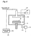
- NF 3 is used as a cleaning gas and NF 3 is introduced into remote plasma generator 101 disposed outside the reaction chamber 102.
- the NF 3 is converted to plasma, and the cleaning gas of NF 3 having been converted to plasma is introduced into the reaction chamber 102 in which a decompression state is maintained, through the raw-material gas supply path 108 and the upper electrode 104. Consequently, the surfaces of the inner wall, electrodes and other parts of the reaction chamber 102 are cleaned.
- this NF 3 gas has high toxicity, the influence on an environment is large and moreover it is expensive, so that cost of a semiconductor product is unfavoraable increased.
- Another object of the present invention is to provide a cleaning device for CVD apparatus used in such a method.
- a method of cleaning a CVD apparatus wherein, a reactive gas is fed into a reaction chamber, a deposited film is formed on a surface of base material disposed in the reaction chamber, said method comprises:
- a cleaning device for CVD apparatus the CVD apparatus being a plasma CVD apparatus wherein a reactive gas is fed into a reaction chamber, a deposited film is formed on a surface of base material disposed in the reaction chamber, said cleaning device comprises:
- a fluorinated cleaning gas containing a fluorocompound is converted to plasma by a remote plasma generator after the film formation and the cleaning gas having been converted to plasma is introduced into the reaction chamber, so that by-products adhered to inner parts of the reaction chamber is removed. Therefore, the dissociation efficiency of cleaning gas is so high that the by-products such as SiO 2 and Si 3 N 4 adhered to and deposited on surfaces of the inner wall, electrodes and other parts of the reaction chamber can be removed efficiently. Moreover, by virtue of the construction, the discharge amount of cleaning gas is so small, the influence on environment such as global warming is little, and cost reduction can be also attained.
- the cleaning method for CVD apparatus according to the present invention is preferably characterized in that the cleaning gas having been converted to plasma is directly introduced into the reaction chamber.
- the cleaning device for CVD apparatus is preferably characterized in that the cleaning gas introduction path is so constructed as to directly introduce the cleaning gas having been converted to plasma into the reaction chamber.
- the cleaning gas having been converted to plasma by the remote plasma generator does not pass the raw material supply path, upper electrode, etc., so that the cleaning gas would not contact or impact with wall parts of such members. Therefore, the efficiency of gasifying the by-products into SiF 4 by reacting the cleaning as with by-products such as SiO 2 , and Si 3 N 4 , which is adehred to and deposited on surfaces of the inner wall, electrodes and other parts of the reaction chamber, would be in no event lowered.
- a distance between the remote plasma generator and the reaction chamber is in the range of 0 to 200 cm.
- the cleaning method for CVD apparatus is preferably characterized in that, when the cleaning gas having been converted to plasma is directly introduced into the reaction chamber, the cleaning gas is introduced through a side part of the reaction chamber.
- the cleaning device for CVD apparatus is preferably characterized in that the cleaning gas introduction path is so constructed that when the cleaning gas having been converted to plasma is directly introduced into the reaction chamber, the cleaning gas is introduced through a side part of the reaction chamber.
- the path for introducing the cleaning gas having been converted to plasma is short and the cleaning gas is directly fed to all over desired sites to be cleaned within the reaction chamber. Therefore, the efficiency of gasifying the by-products into SiF 4 by reacting the cleaning gas with by-products such as SiO 2 and Si 3 N 4 which is adhered to and deposited on surfaces of the inner wall, electrodes and other parts of the reaction chamber can be improved.
- a flow rate of the cleaning gas introduced into the reaction chamber is 0.1 to 100 L/min.
- the pressure of cleaning gas in the reaction chamber is in the range of 10 to 2000 Pa.
- the cleaning method for CVD apparatus according to the present invention is characterized in that:
- the cleaning device for CVD apparatus is characterized in that the cleaning gas introduction path includes:
- the cleaning gas having been converted to plasma is introduced directly into the reaction chamber and the cleaning gas is introduced into the reaction chamber through a raw-material gas supply path.
- the efficiency of gasifying the by-products into SifF 4 by reacting the cleaning gas with by-products such as SiO 2 and Si 3 N 4 would be further improved.
- the cleaning method for CVD apparatus is characterized in that a selective switching is performed between the direct introduction of the cleaning gas having been converted to plasma into the reaction chamber and the introduction of the cleaning gas having been converted to plasma into the reaction chamber through the raw gas supply path.
- the cleaning device for CVD apparatus is characterized in that it further comprises a switching controller capable of performing a selective switching between the first cleaning gas introduction path and the second cleaning gas introduction path.
- the fluorocompound is at least one member selected from the group consisting of nitrogenous fluorocompounds, oxygen-containing perfluorocarbons and perfluorocarbons having 1 to 6 carbon atoms. Still preferably, the fluorocompound is a perfluorocarbon having 1 to 6 carbon atoms.
- perfluorocarbons means compounds consisting of various functional groups and fluorinated carbon compounds, such as chain aliphatic, linear ether, cyclic ether and unsaturated (including diene) compounds and compounds containing oxygen in the molecules thereof.
- the dissociation efficiency of cleaning gas is so high that the by-products such as SiO 2 and Si 3 N 4 adhered to and deposited on surfaces of the inner wall, electrodes and other parts of the reaction chamber can be removed efficiently.
- the discharge amount of cleaning gas is so small that the influence on environment such as global warming is little and cost reduction can be attained.
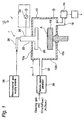
- FIG. 1 is a schematic view showing the first embodiment wherein the cleaning device for CVD apparatus used in carrying out the cleaning method for CVD apparatus according to the present invention has been applied to a plasma CVD method.
- cleaning device 11 for plasma CVD apparatus 10 includes reaction chamber 12 wherein a vacuum (reduced pressure) is maintained.
- the reaction chamber 12 at its bottom wall 12c is provided with exhaust path 16, through which the inside gas is discharged outside by means of pump 14.
- a given vacuum decompression state
- the reaction chamber 12 in its interior is provided with lower electrode 18 which constitutes a stage for mounting base material A, such as silicon wafer, on which at an upper surface a silicon thin film is deposited (e.g., vapor deposited).
- the lower electrode 18 is passed through the bottom wall 12c of the reaction chamber 12 and is vertically slidable by means of driving means (not shown) .
- driving means not shown
- the lower electrode 18 is capable of regulating its position.
- Slide portion between the lower electrode 18 and the bottom wall 12c is provided with a seal member such as a seal ring(not shown) so that a vacuum can be ensured inside the reaction chamber 12.
- an upper electrode 20 is disposed at an upper part of the reaction chamber 12.
- Base end portion 22 of the upper electrode 20 is passed through top wall 12a of the reaction chamber 12, and is connected to high frequency power source 24 disposed outside the reaction chamber 12.
- the upper electrode 20 is provided with high frequency applicator 25, such as a high frequency application coil (not shown).
- a matching circuit (not shown) is disposed between the high frequency applicator 25 and the high frequency power source 24.
- the upper electrode 20 is provided with raw-material gas supply path 26.
- the raw-material gas from raw-material gas supply source 28 is introduced into the reaction chamber 12 in which a decompression state is maintained, through the raw-material gas supply path 26 and the upper electrode 20.
- a remote plasma generator 30 capable of converting a fluorinated cleaning gas containing a fluorocompound to plasma is provided with the side portion of the reaction chamber 12. Furthermore, the cleaning gas having been converted to plasma by the remote plasma generator 30 is introduced into the reaction chamber 12 from side wall 12b through connecting piping 32 constituting a gas introduction path.
- the plasma CVD apparatus 10 of the above construction according to the present invention is operated in the following manner.
- base material A such as a silicon wafer, on which at an upper surface a silicon thin film is to be vapor deposited, is mounted on the stage of the lower electrode 18 of the reaction chamber 12.
- the distance between the base material A and the upper electrode 20 is regulated to predetermined distance by driving means (not shown).
- the raw-material gas is introduced into the reaction chamber 12, in which a decompression state is maintained, from the raw-material gas supply source 28 through the raw-material gas supply path 26 and the upper electrode 20.
- the raw-material gas fed from the raw-material gas supply source 28 for example, it is appropriate to feed monosilane (SiH 4 ), N 2 O, N 2 , O 2 , Ar, etc., as raw-material gas, in the formation of a thin filmof silicon oxide (SiO 2 ).
- a thin film of silicon nitride e.g., Si 3 N 4
- the raw-material gas is not limited to these and can be appropriately changed depending on the type of thin film to be formed or the like.
- disilane Si 2 H 6
- TEOS tetraethoxysilane: Si(OC 2 H 5 ) 4
- O 2 or O 3 a raw-material gas
- High frequency power outputted from the high frequency power source 24 is propagated to the high frequency applicator 25, such as a high frequency application coil, whereby the high frequency power is applied to the upper electrode 20.
- the high frequency applicator 25 such as a high frequency application coil
- the high frequency power is applied to the upper electrode 20.
- a high frequency electric field is generated by the upper electrode 20.
- electrons impact with neutral molecules of raw-material gas so that a high frequency plasma is generated.
- the raw-material gas is dissociated into ions and radicals.
- a silicon thin film compound is formed on a surface of base material A such as silicon wafer mounted on the lower electrode 18.
- this plasma CVD apparatus 10 at the stage of film formation, electric discharge within the reaction chamber 12 would cause a thin film material such as SiO 2 or Si 3 N 4 to adhere to and deposit on surfaces other than the surface of semiconductor article A on which film formation is to be conducted, for example, those of the inner wall and electrodes of the reaction chamber 12, so that by-products would occur. When such by-products grow to a certain thickness, the by-products would be detached and dissipated by the self weight thereof or a stress caused thereby. These, at the time of film formation, would cause mixing of fine particles as foreign matter into semiconductor products and hence contamination of the semiconductor products. Therefore, this plasma CVD apparatus 10 cannot produce a thin film of high quality and has had the danger of causing breakage of semiconductor circuits or shortcircuiting thereof and also causing, for example, yield drop.
- a thin film material such as SiO 2 or Si 3 N 4
- the fluorinated cleaning gas containing a fluorocompound is converted to plasma by means of the remote plasma generator 30. Then, the resultant cleaning gas is introduced into the reaction chamber 12 in which a decompression state is maintained, through the connecting piping 32.
- a high frequency plasma is geneated, and, in the high frequency plasma, the cleaning gas is dissociated into ions and radicals. These ions and radicals react with by-products such as SiO 2 and Si 3 N 4 adhered to and deposited on surfaces of the inner wall, electrodes and other parts of the reaction chamber 12 so that the by-products into SiF 4 is gasified.
- the resultant gas together with exhaust gas is discharged outside the reaction chamber 12 through the exhaust path 16 by means of the pump 14.
- perfluorocarbons having 1 to 6 carbon atoms including:
- oxygen-containing perfluorocarbons such as COF 2 , CF 3 COF and CF 3 OF
- nitrogenous fluorocompounds such as FNO, F 3 NO and FNO 2
- oxygen-containing nitrogenous fluorocompounds can be used.
- fluorocompounds may be those having at least one fluorine atom which result from partial replacement of the fluorine atoms by hydrogen atoms.
- fluorine atoms may be those having at least one fluorine atom which result from partial replacement of the fluorine atoms by hydrogen atoms.
- the use of CF 4 , C 2 F 6 or C 3 F 8 is preferred.
- the use of CF 4 or C 2 F 6 is still preferred.
- the cleaning gas containing a fluorocompound for use in the present invention can appropriately be used in combination with another gas as long as it is not detrimental to the effects exerted by the present invention.
- another gas for example, He, Ne, Ar or O 2 .
- the amount of other gas mixed with the fluorinated cleaning gas is not particularly limited, and can be determined taking into account, for example, the amount and thickness of by-products (deposits) adhered to the inner wall and other parts of the reaction chamber 12 of the CVD apparatus 10, the type of fluorocompound employed and the composition of by-products can be used.
- silicic compounds adhered to, for example, CVD chamber walls and CVD apparatus jigs in the CVD method or the like.
- silicic compound deposits include those of at least one member selected from among:
- the flow rate of cleaning gas introduced into the reaction chamber 12 is in the range of 0.1 to 100 L/min, preferably 0.5 to 10 L/min. The reason is that, when the flow rate of cleaning gas introduced into the reaction chamber 12 is less than 0.1 L/min, the above cleaning effect cannot be anticipated. On the other hand, when the flow rate is greater than 100 L/min, the amount of cleaning gas discharged outside without contributing to cleaning becomes unfavorably large.
- the flow rate of cleaning gas introduced can be appropriately changed depending on, for example, the type and size of base material A such as a flat panel disk or the like. For instance, when the fluorocompound is C 2 F 6 , it is appropriate to set the flow rate for 0.5 to 5 L/min.
- the pressure of cleaning gas in the reaction chamber 12 is in the range of 10 to 2000 Pa, preferably 50 to 100 Pa. The reason is that, when the pressure of cleaning gas in the reaction chamber 12 is lower than 10 Pa or greater than 2000 Pa, the above cleaning effect cannot be anticipated.
- the pressure of cleaning gas in the reaction chamber 12 can be appropriately changed depending on, for example, the type and size of base material A such as a flat panel disk or the like. For instance, when the fluorocompound is C 2 F 6 , it is appropriate to set the pressure for 100 to 500 Pa.
- the distance between the remote plasma generator 30 and the reaction chamber 12, namely, the length L of connecting piping 32 is in the range of 0 to 200 cm, preferably 0 to 100 cm, and still preferably 0 to 50 cm.
- the reason is that, when the length L is greater than 200 cm, the cleaning gas having been converted to plasma would contact and impact with wall portions of the connecting piping 32 with the result that the efficiency of gasifying the by-products would be lowered.
- the length L although the smaller the better, can appropriately be determined depending on, for example, the type and size of base material A.
- the material of connecting piping 32 is not particularly limited, it is preferred from the viewpoint of the effect of preventing the drop of gasification efficiency that the material is selected from among, for example, alumina, inactivated aluminum, a fluororesin and a metal coated with a fluororesin.
- the remote plasma generator 30 and the reaction chamber 12 have been so arranged that the cleaning gas having been converted to plasma is passed through the connecting piping 32 and introduced into the reaction chamber 12 at the chamber side wall 12b.
- this arrangement is not limitative as long as the cleaning gas is directly introduced into the reaction chamber 12.
- the cleaning gas can be introduced into the reaction chamber 12 at its top wall 12a or at its bottom wall 12c.
- the introduction into the reaction chamber 12 may be effected from positions of different heights of the chamber side wall 12b. Still further, although not shown, these may be combined.
- the remote plasma generator 30 is not particularly limited, and known remote plasma generators can be used.
- "ASTRON" manufactured by ASTEX can be used.
- the construction of this Embodiment of the present invention is such that, after the film formation, the fluorinated cleaning gas containing a fluorocompound is converted to plasma by the remote plasma generator 30 and thereafter the cleaning gas having been converted to plasma is introduced into the reaction chamber 12 so that by-products adhered to inner parts of the reaction chamber 12 are removed. Consequently, the dissociation efficiency of cleaning gas is so high that the by-products such as SiO 2 and Si 3 N 4 adhered to and deposited on surfaces of the inner wall, electrodes and other parts of the reaction chamber 12 can be removed efficiently. Moreover, the discharge amount of cleaning gas is so small that the influence on environment such as global warming is little and cost reduction can be attained.
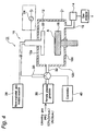
- Fig. 4 is a schematic view showing the second embodiment wherein the cleaning device for CVD apparatus used in carrying out the cleaning method for CVD apparatus according to the present invention has been applied to a plasma CVD apparatus.
- the cleaning device 11 for plasma CVD apparatus 10 has fundamentally the same construction as that of the cleaning device 11 for plasma CVD apparatus 10 shown in Fig. 1. Through Figs. 1 and 4, like reference numbers are assigned to like constituent members, and detailed explanation thereof would not be repeated.
- the cleaning device 11 for plasma CVD apparatus 10 is provided with connecting piping 32 which functions as a first cleaning gas introduction path adapted to directly introduce the cleaning gas having been converted to plasma by the remote plasma generator 30 into the reaction chamber 12 at its chamber side wall 12b.
- the cleaning device 11 is also provided with connecting piping 33 which functions as a second cleaning gas introduction path adapted to introduce the cleaning gas having been converted to plasma by the remote plasma generator 30 into the reaction chamber 12 through the raw-material gas supply path 26 and through the upper electrode 20.
- This construction designed to directly introduce the cleaning gas having been converted to plasma into the reaction chamber 12 through the connecting piping 32 which functions as a first cleaning gas introduction path.
- This construction designed to effect the introduction into the reaction chamber 12 through the connecting piping 33 which functions as a second cleaning gas introduction path adapted to introduce the cleaning gas through the raw gas supply path 26 and the upper electrode 20. Therefore, the efficiency of gasifying the by-products into SiF4 by reacting the cleaning gas with by-products such as SiO 2 and Si 3 N 4 adhered to and deposited on surfaces of the inner wall, electrodes and other parts of the reaction chamber 12.
- the cleaning device 11 further comprise switching controller 40 capable of performing a selective switching between the connecting piping 32 as the first cleaning gas introduction path and the connecting piping 33 as the second cleaning gas introduction path.
- switching controller 40 capable of performing a selective switching between the connecting piping 32 as the first cleaning gas introduction path and the connecting piping 33 as the second cleaning gas introduction path.
- the present invention can also be applied to other CVD methods, for example, the vacuum deposition method wherein a thin film is deposited on a base material through the thermal decomposition, oxidation, reduction, polymerization, vaporization reaction, etc. of a thin film material at high temperatures.
- the vacuum deposition method wherein a thin film is deposited on a base material through the thermal decomposition, oxidation, reduction, polymerization, vaporization reaction, etc. of a thin film material at high temperatures.
- a base material (silicon substrate of 725 ⁇ m thickness and 2000 mm diameter) was mounted on the lower electrode 18, using the CVD apparatus 10 of Fig. 1.
- raw-material reactive gas specifically, monosilane gas 180 SCCM, ammonia 320 SCCM and N 2 1 L/min were fed into the reaction chamber 12.
- the pressure inside the reaction chamber 12 was maintained at 320 Pa, and high frequency power of 520 W output from a 13.65 MHz high frequency power source was applied to the upper electrode 20. Under these conditions, film formation was performed for 40 sec so that a thin film of 7000 to 8000 ⁇ was obtained.
- cleaning according to the prior art was performed by, as shown in Fig. 6, cleaning gas of 260 Pa pressure consisting of NF 3 /Ar (gas flow rates 500/500 (SCCM)) is converted to plasma by means of the remote plasma generator 101. Then, the cleaning gas having been converted to plasma is introduced into the reaction chamber 102 in which a decompression state was maintained, through the gas supply path 108 and the upper electrode 104. The gas discharge amount and time required for chamber cleaning were measured in the above manner.
- cleaning gas of 260 Pa pressure consisting of NF 3 /Ar (gas flow rates 500/500 (SCCM))
- SCCM gas flow rates 500/500
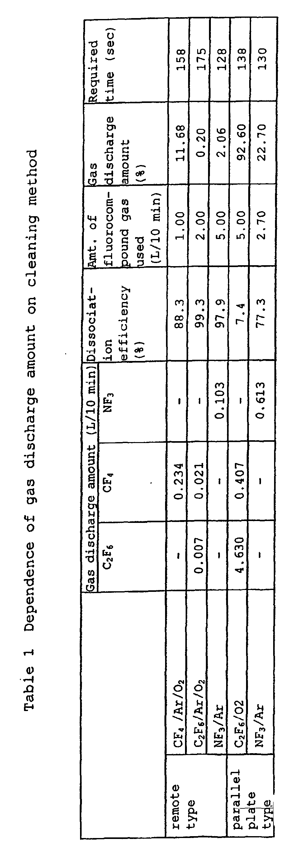
- the gas discharge amount is high, the gas discharge amount is high, and the efficiency of dissociation of cleaning gas, which contributes to intended cleaning, into ions and radicals is low.
- the gas discharge amount is low, the gas discharge amount is low, and the efficiency of dissociation of cleaning gas, which contributes to intended cleaning, into ions and radicals is high.
- the time required for chamber cleaning there is no marked difference between the remote plasma type cleaning method according to the present invention and the conventional parallel plate type plasma cleaning method.
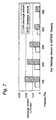
- the cleaning method of the present invention was carried out with the use of cleaning gas consisting of C 2 F 6 /Ar/O 2 (gas flow rates 100/1600/400 (SCCM)) in the same manner as in Example 1, except that the cleaning pressure was varied within the range of 130 to 600 Pa, and the gas discharge amounts were measured. The results are shown in the graph of Fig. 7.
- the fluorinated cleaning gas containing a fluorocompound is converted to plasma by the remote plasma generator after the film formation. Then, the cleaning gas having been converted to plasma is introduced into the reaction chamber so that by-products adhered to inner parts of the reaction chamber is removed. Therefore, the dissociation efficiency of cleaning gas is so high that the by-products such as SiO 2 and Si 3 N 4 adhered to and deposited on surfaces of the inner wall, electrodes and other parts of the reaction chamber can be removed efficiently. Moreover, by virtue of the construction, the discharge amount of cleaning gas is so small that the influence on environment such as global warming is little and cost reduction can be also attained.
- the cleaning gas having been converted to plasma by the remote plasma generator does not pass through the raw material supply path, upper electrode, etc.
- the cleaning gas having been converted to plasma would not impact and contact with wall parts of such members. Therefore, the efficiency of gasifying the by-products into SiF 4 by reacting the cleaning gas with by-products such as SiO 2 and Si 3 N 4 , which is adhered to and deposited on surfaces of the inner wall, electrodes and other parts of the reaction chamber, would be in no event lowered.
- the cleaning gas for use in the present invention contains a fluorocompound.
- a fluorocompound for example, nitrogenous fluorocompounds, oxygen-containing perfluorocarbons and perfluorocarbons having 1 to 6 carbon atoms can be used.
- the dissociation efficiency of cleaning gas is so high that the by-products such as SiO 2 and Si 3 N 4 adhered to and deposited on surfaces of the inner wall, electrodes and other parts of the reaction chamber can be removed efficiently.
- the discharge amount of cleaning gas is so small that the influence on environment such as global warming is little and cost reduction can be also attained.
- the present invention can exert a variety of striking peculiar functions and effects.
Landscapes
- Chemical & Material Sciences (AREA)
- General Chemical & Material Sciences (AREA)
- Chemical Kinetics & Catalysis (AREA)
- Engineering & Computer Science (AREA)
- Materials Engineering (AREA)
- Mechanical Engineering (AREA)
- Metallurgy (AREA)
- Organic Chemistry (AREA)
- Chemical Vapour Deposition (AREA)
- Drying Of Semiconductors (AREA)
- Electrical Discharge Machining, Electrochemical Machining, And Combined Machining (AREA)
- Cleaning Or Drying Semiconductors (AREA)
- Plasma Technology (AREA)
- Physical Or Chemical Processes And Apparatus (AREA)
- Crystals, And After-Treatments Of Crystals (AREA)
Abstract
Description
which is a method wherein a solid thin film material is converted to atoms or atomic groups by physical means and deposited on a surface for film formation to thereby form a thin film;
which is a method wherein a gaseous thin film material is heated to high temperature so as to induce chemical reaction, thereby forming a thin film; and
which is a method wherein a gaseous thin film material is converted to plasma so as to induce chemical reaction, thereby forming a thin film.
Claims (18)
- Amethod of cleaning a CVD apparatus wherein, a reactive gas is fed into a reaction chamber, a deposited film is formed on a surface of basematerial disposed in the reaction chamber, said method comprises:converting a fluorinated cleaning gas containing a fluorcompound to plasma by means of a remote plasma generator after the deposited film formation on the base material surface by the use of the CVD apparatus, andintroducing the cleaning gas having been converted to plasma into the reaction chamber to thereby remove any by-products sticking to inner parts of the reaction chamber.
- The cleaning method as claimed in claim 1, wherein the cleaning gas having been converted to plasma is directly introduced into the reaction chamber.
- The cleaning method as claimed in claim 1 or 2, wherein, when the cleaning gas having been converted to plasma is directly introduced into the reaction chamber, distance between the remote plasma generator and the reaction chamber is in the range of 0 to 200 cm.
- The cleaning method as claimed in claim 2 or 3, wherein, when the cleaning gas having been converted to plasma is directly introduced into the reaction chamber, the cleaning gas is introduced through a side part of the reaction chamber.
- The cleaning method as claimed in any of claims 1 to 4, wherein:the cleaning gas having been converted to plasma is directly introduced into the reaction chamber, andthe cleaning gas having been converted to plasma is introduced into the reaction chamber through a raw-material gas supply path.
- The cleaning method as claimed in claim 5, wherein a selective switching is performed between the direct introduction of the cleaning gas having been converted to plasma into the reaction chamber and the introduction of the cleaning gas having been converted to plasma into the reaction chamber through the raw gas supply path.
- The cleaning method as claimed in any of claims 1 to 6, wherein the fluorocompound is at least one member selected from the group consisting of nitrogenous fluorocompounds, oxygen-containing perfluorocarbons and perfluorocarbons having 1 to 6 carbon atoms.
- The cleaning method as claimed in any of claims 1 to 7, wherein the fluorocompound is a perfluorocarbon having 1 to 6 carbon atoms.
- The cleaning method as claimed in any of claims 1 to 8, wherein the CVD apparatus is a plasma enhanced CVD apparatus having an upper electrode and a lower electrode both arranged inside a reaction chamber, between which a radiofrequency power is applied to thereby generate plasma, so that a deposited film is formed on a surface of base material disposed on the lower electrode inside the reaction chamber.
- A cleaning device for CVD apparatus, the CVD apparatus being a plasma CVD apparatus wherein a reactive gas is fed into a reaction chamber, a deposited film is formed on a surface of base material disposed in the reaction chamber, said cleaning device comprises:a remote plasma generator capable of converting a fluorinated cleaning gas containing a fluorocompound to plasma after the deposited film formation on the base material surface by the use of the plasma CVD apparatus; anda cleaning gas introduction path for introducing the cleaning gas having been converted to plasma by means of the remote plasma generator into the reaction chamber,so that by-products adhered to inner parts of the reaction chamber are removed by the cleaning gas having been introduced into the reaction chamber.
- The cleaning device for CVD apparatus as claimed in claim 10, wherein the cleaning gas introduction path is so constructed as to directly introduce the cleaning gas having been converted to plasma into the reaction chamber.
- The cleaning device for CVD apparatus as claimed in claim 10 or 11, wherein, when the cleaning gas having been converted to plasma into the reaction chamber, a distance between the remote plasma generator and the reaction chamber is in the range of 0 to 200 cm.
- The cleaning device for CVD apparatus as claimed in claim 11 or 12, wherein the cleaning gas introduction path is so constructed that when the cleaning gas having been converted to plasma is directly introduced into the reaction chamber, the cleaning gas in introduced through a side part of the reaction chamber.
- The cleaning device for CVD apparatus as claimed in any of claims 10 to 13, wherein the cleaning gas introduction path includes:a first cleaning gas introduction path for directly introducing the cleaning gas having been converted to plasma into the reaction chamber, anda second cleaning gas introduction path for introducing the cleaning gas having been converted to plasma into the reaction chamber through a raw-material gas supply path.
- The cleaning device for CVD apparatus as claimed in claim 14, which further comprises a switching controller capable of performing a selective switching between the first cleaning gas introduction path and the second cleaning gas introduction path.
- The cleaning device for CVD apparatus as claimed in any of claims 10 to 15, wherein the fluorocompound is at least one member selected from the group consisting of nitrogenous fluorocompounds, oxygen-containing perfluorocarbons and perfluorocarbons having 1 to 6 carbon atoms.
- The cleaning device for CVD apparatus as claimed in any of claims 10 to 16, wherein the fluorocompound is a perfluorocarbon having 1 to 6 carbon atoms.
- The cleaning device for CVD apparatus as claimed in any of claims 10 to 17, wherein the CVD apparatus is a plasma CVD apparatus having an upper electrode and a lower electrode both arranged inside a reaction chamber, the reaction chamber adapted to generate plasma upon application of a high frequency power between the upper electrode and the lower electrode to thereby form a deposited film on a surface of base material disposed on the lower electrode inside the reaction chamber.
Applications Claiming Priority (3)
| Application Number | Priority Date | Filing Date | Title |
|---|---|---|---|
| JP2001082840A JP2002280376A (en) | 2001-03-22 | 2001-03-22 | Cleaning method for CVD apparatus and cleaning apparatus therefor |
| JP2001082840 | 2001-03-22 | ||
| PCT/JP2002/002548 WO2002078073A1 (en) | 2001-03-22 | 2002-03-18 | Method of cleaning cvd device and cleaning device therefor |
Publications (3)
| Publication Number | Publication Date |
|---|---|
| EP1304731A1 true EP1304731A1 (en) | 2003-04-23 |
| EP1304731A4 EP1304731A4 (en) | 2003-07-30 |
| EP1304731B1 EP1304731B1 (en) | 2006-08-02 |
Family
ID=18938735
Family Applications (1)
| Application Number | Title | Priority Date | Filing Date |
|---|---|---|---|
| EP02705296A Expired - Lifetime EP1304731B1 (en) | 2001-03-22 | 2002-03-18 | Method of cleaning cvd device and cleaning device therefor |
Country Status (8)
| Country | Link |
|---|---|
| US (1) | US6935351B2 (en) |
| EP (1) | EP1304731B1 (en) |
| JP (1) | JP2002280376A (en) |
| KR (1) | KR100523069B1 (en) |
| AT (1) | ATE335285T1 (en) |
| DE (1) | DE60213536T2 (en) |
| TW (1) | TW554418B (en) |
| WO (1) | WO2002078073A1 (en) |
Cited By (8)
| Publication number | Priority date | Publication date | Assignee | Title |
|---|---|---|---|---|
| WO2004066365A3 (en) * | 2003-01-16 | 2004-11-04 | Applied Materials Inc | Cleaning of cvd chambers using remote source with cxfyoz based chemistry |
| US6902629B2 (en) | 2002-04-12 | 2005-06-07 | Applied Materials, Inc. | Method for cleaning a process chamber |
| WO2005090638A3 (en) * | 2004-03-24 | 2006-04-13 | Du Pont | Remote chamber methods for removing surface deposits |
| EP1318542A4 (en) * | 2000-09-11 | 2006-10-25 | Nat Inst Of Advanced Ind Scien | CLEANING GAS AND ATTACK GAS |
| EP1475822A4 (en) * | 2002-02-12 | 2007-04-25 | Res Inst Innovative Tech Earth | CLEANING GAS AND ETCHING GAS |
| EP1991373A4 (en) * | 2006-02-21 | 2009-07-01 | Applied Materials Inc | IMPROVING REMOTE PLASMA SOURCES FOR CLEANING DIELECTRIC FILMS |
| US7947129B2 (en) * | 2003-06-06 | 2011-05-24 | Sen Corporation, An Shi And Axcelis Company | Ion source apparatus and cleaning optimized method thereof |
| US8679989B2 (en) | 2006-03-27 | 2014-03-25 | Hitachi Kokusai Electric Inc. | Method of manufacturing semiconductor device including removal of deposits from process chamber and supply portion |
Families Citing this family (39)
| Publication number | Priority date | Publication date | Assignee | Title |
|---|---|---|---|---|
| JP2003197615A (en) * | 2001-12-26 | 2003-07-11 | Tokyo Electron Ltd | Plasma processing apparatus and cleaning method thereof |
| WO2003088845A2 (en) * | 2002-04-16 | 2003-10-30 | Tyco Healthcare Group, Lp | Surgical stapler and method |
| JP2004179426A (en) * | 2002-11-27 | 2004-06-24 | Tokyo Electron Ltd | Cleaning method for substrate processing equipment |
| US20040129223A1 (en) * | 2002-12-24 | 2004-07-08 | Park Jong Hyurk | Apparatus and method for manufacturing silicon nanodot film for light emission |
| JP4320389B2 (en) * | 2003-02-28 | 2009-08-26 | 関東電化工業株式会社 | CVD chamber cleaning method and cleaning gas used therefor |
| JP4264479B2 (en) * | 2003-03-14 | 2009-05-20 | キヤノンアネルバ株式会社 | Cleaning method for CVD apparatus |
| JP4385086B2 (en) * | 2003-03-14 | 2009-12-16 | パナソニック株式会社 | CVD apparatus cleaning apparatus and CVD apparatus cleaning method |
| US20050014383A1 (en) * | 2003-07-15 | 2005-01-20 | Bing Ji | Use of hypofluorites, fluoroperoxides, and/or fluorotrioxides as oxidizing agent in fluorocarbon etch plasmas |
| US20080223409A1 (en) * | 2003-12-12 | 2008-09-18 | Horsky Thomas N | Method and apparatus for extending equipment uptime in ion implantation |
| US20050258137A1 (en) * | 2004-03-24 | 2005-11-24 | Sawin Herbert H | Remote chamber methods for removing surface deposits |
| US7581549B2 (en) | 2004-07-23 | 2009-09-01 | Air Products And Chemicals, Inc. | Method for removing carbon-containing residues from a substrate |
| US20060021633A1 (en) * | 2004-07-27 | 2006-02-02 | Applied Materials, Inc. | Closed loop clean gas control |
| JP2006114780A (en) * | 2004-10-15 | 2006-04-27 | Tokyo Electron Ltd | Thin film forming apparatus cleaning method, thin film forming apparatus, and program |
| US20060144819A1 (en) * | 2004-12-30 | 2006-07-06 | Sawin Herbert H | Remote chamber methods for removing surface deposits |
| US20060144820A1 (en) * | 2004-12-30 | 2006-07-06 | Sawin Herbert H | Remote chamber methods for removing surface deposits |
| KR100712529B1 (en) * | 2005-09-02 | 2007-04-30 | 삼성전자주식회사 | In-situ cleaning method of plasma applicator and plasma applicator employing the cleaning method |
| US20070107750A1 (en) * | 2005-11-14 | 2007-05-17 | Sawin Herbert H | Method of using NF3 for removing surface deposits from the interior of chemical vapor deposition chambers |
| US7862683B2 (en) * | 2005-12-02 | 2011-01-04 | Tokyo Electron Limited | Chamber dry cleaning |
| KR100765128B1 (en) | 2006-05-30 | 2007-10-11 | 주식회사 아토 | Cleaning apparatus and method of the CD chamber |
| KR100819096B1 (en) * | 2006-11-21 | 2008-04-02 | 삼성전자주식회사 | Cleaning Method Using Remote Plasma in Semiconductor Manufacturing Equipment |
| KR100855002B1 (en) * | 2007-05-23 | 2008-08-28 | 삼성전자주식회사 | Plasma ion implantation system |
| JP4933979B2 (en) * | 2007-08-10 | 2012-05-16 | 株式会社アルバック | Cleaning method for film forming apparatus |
| US7699935B2 (en) * | 2008-06-19 | 2010-04-20 | Applied Materials, Inc. | Method and system for supplying a cleaning gas into a process chamber |
| US20110114114A1 (en) * | 2008-07-14 | 2011-05-19 | Ips Ltd. | Cleaning method of apparatus for depositing carbon containing film |
| JP2011228546A (en) * | 2010-04-21 | 2011-11-10 | Mitsubishi Electric Corp | Plasma cvd apparatus and cleaning method therefor |
| CN112981369B (en) * | 2013-12-30 | 2023-11-10 | 科慕埃弗西有限公司 | Chamber Cleaning and Semiconductor Etching Gases |
| JP5941491B2 (en) * | 2014-03-26 | 2016-06-29 | 株式会社日立国際電気 | Substrate processing apparatus, semiconductor device manufacturing method, and program |
| KR101577782B1 (en) * | 2014-05-29 | 2015-12-16 | 참엔지니어링(주) | Apparatus and Method for Processing Substrate |
| US20160032451A1 (en) * | 2014-07-29 | 2016-02-04 | Applied Materials, Inc. | Remote plasma clean source feed between backing plate and diffuser |
| CN106373868B (en) * | 2016-10-10 | 2020-03-10 | 昆山龙腾光电股份有限公司 | A manufacturing method of an array substrate |
| JP2019033236A (en) | 2017-08-10 | 2019-02-28 | 株式会社日本製鋼所 | Atomic layer growth apparatus, method for film formation using the same, and cleaning method thereof |
| TWI912719B (en) * | 2018-07-09 | 2026-01-21 | 美商蘭姆研究公司 | Switch, power supply system, substrate processing system, and method for supplying power |
| US10751765B2 (en) * | 2018-08-13 | 2020-08-25 | Applied Materials, Inc. | Remote plasma source cleaning nozzle for cleaning a gas distribution plate |
| KR20230088869A (en) * | 2020-10-23 | 2023-06-20 | 램 리써치 코포레이션 | Integration of the vapor deposition process into the plasma etch reactor |
| JP7706236B2 (en) | 2020-12-25 | 2025-07-11 | 東京エレクトロン株式会社 | Plasma Processing Equipment |
| US11772137B2 (en) * | 2021-07-23 | 2023-10-03 | Applied Materials, Inc. | Reactive cleaning of substrate support |
| US20230307216A1 (en) * | 2022-03-25 | 2023-09-28 | Applied Materials, Inc. | Enhanced chamber clean and recovery with dual flow path |
| JP2023183383A (en) * | 2022-06-15 | 2023-12-27 | セメス カンパニー,リミテッド | Substrate processing equipment and substrate processing method |
| CN115142127B (en) * | 2022-08-29 | 2022-11-18 | 一道新能源科技(泰州)有限公司 | Polycrystalline silicon forming furnace based on LPCVD |
Family Cites Families (12)
| Publication number | Priority date | Publication date | Assignee | Title |
|---|---|---|---|---|
| DE3725358A1 (en) * | 1987-07-30 | 1989-02-09 | Telog Systems Gmbh | DEVICE AND METHOD FOR SURFACE TREATMENT OF MATERIALS |
| US5647945A (en) * | 1993-08-25 | 1997-07-15 | Tokyo Electron Limited | Vacuum processing apparatus |
| JPH07335563A (en) | 1994-06-10 | 1995-12-22 | Mitsubishi Electric Corp | Plasma CVD equipment |
| EP0697467A1 (en) * | 1994-07-21 | 1996-02-21 | Applied Materials, Inc. | Method and apparatus for cleaning a deposition chamber |
| US6071572A (en) * | 1996-10-15 | 2000-06-06 | Applied Materials, Inc. | Forming tin thin films using remote activated specie generation |
| US5935340A (en) * | 1996-11-13 | 1999-08-10 | Applied Materials, Inc. | Method and apparatus for gettering fluorine from chamber material surfaces |
| US6274058B1 (en) * | 1997-07-11 | 2001-08-14 | Applied Materials, Inc. | Remote plasma cleaning method for processing chambers |
| JP2001020076A (en) * | 1999-07-06 | 2001-01-23 | Hitachi Kokusai Electric Inc | Method and apparatus for cleaning reaction chamber |
| US6255222B1 (en) | 1999-08-24 | 2001-07-03 | Applied Materials, Inc. | Method for removing residue from substrate processing chamber exhaust line for silicon-oxygen-carbon deposition process |
| KR100767762B1 (en) * | 2000-01-18 | 2007-10-17 | 에이에스엠 저펜 가부시기가이샤 | A CVD semiconductor-processing device provided with a remote plasma source for self cleaning |
| US6835278B2 (en) * | 2000-07-07 | 2004-12-28 | Mattson Technology Inc. | Systems and methods for remote plasma clean |
| JP2002057106A (en) | 2000-08-08 | 2002-02-22 | Tokyo Electron Ltd | Processing apparatus cleaning method and processing apparatus |
-
2001
- 2001-03-22 JP JP2001082840A patent/JP2002280376A/en active Pending
-
2002
- 2002-03-18 WO PCT/JP2002/002548 patent/WO2002078073A1/en not_active Ceased
- 2002-03-18 DE DE60213536T patent/DE60213536T2/en not_active Expired - Lifetime
- 2002-03-18 EP EP02705296A patent/EP1304731B1/en not_active Expired - Lifetime
- 2002-03-18 US US10/276,305 patent/US6935351B2/en not_active Expired - Lifetime
- 2002-03-18 KR KR10-2002-7015744A patent/KR100523069B1/en not_active Expired - Lifetime
- 2002-03-18 AT AT02705296T patent/ATE335285T1/en not_active IP Right Cessation
- 2002-03-21 TW TW091105410A patent/TW554418B/en not_active IP Right Cessation
Cited By (11)
| Publication number | Priority date | Publication date | Assignee | Title |
|---|---|---|---|---|
| EP1318542A4 (en) * | 2000-09-11 | 2006-10-25 | Nat Inst Of Advanced Ind Scien | CLEANING GAS AND ATTACK GAS |
| EP1475822A4 (en) * | 2002-02-12 | 2007-04-25 | Res Inst Innovative Tech Earth | CLEANING GAS AND ETCHING GAS |
| US6902629B2 (en) | 2002-04-12 | 2005-06-07 | Applied Materials, Inc. | Method for cleaning a process chamber |
| WO2004066365A3 (en) * | 2003-01-16 | 2004-11-04 | Applied Materials Inc | Cleaning of cvd chambers using remote source with cxfyoz based chemistry |
| US6923189B2 (en) | 2003-01-16 | 2005-08-02 | Applied Materials, Inc. | Cleaning of CVD chambers using remote source with cxfyoz based chemistry |
| US7947129B2 (en) * | 2003-06-06 | 2011-05-24 | Sen Corporation, An Shi And Axcelis Company | Ion source apparatus and cleaning optimized method thereof |
| WO2005090638A3 (en) * | 2004-03-24 | 2006-04-13 | Du Pont | Remote chamber methods for removing surface deposits |
| WO2005098086A3 (en) * | 2004-03-24 | 2006-05-04 | Du Pont | Remote chamber methods for removing surface deposits |
| WO2005095670A3 (en) * | 2004-03-24 | 2006-05-04 | Du Pont | Remote chamber methods for removing surface deposits |
| EP1991373A4 (en) * | 2006-02-21 | 2009-07-01 | Applied Materials Inc | IMPROVING REMOTE PLASMA SOURCES FOR CLEANING DIELECTRIC FILMS |
| US8679989B2 (en) | 2006-03-27 | 2014-03-25 | Hitachi Kokusai Electric Inc. | Method of manufacturing semiconductor device including removal of deposits from process chamber and supply portion |
Also Published As
| Publication number | Publication date |
|---|---|
| ATE335285T1 (en) | 2006-08-15 |
| KR100523069B1 (en) | 2005-10-24 |
| KR20030007668A (en) | 2003-01-23 |
| DE60213536T2 (en) | 2007-10-25 |
| EP1304731A4 (en) | 2003-07-30 |
| US20030079757A1 (en) | 2003-05-01 |
| WO2002078073A1 (en) | 2002-10-03 |
| DE60213536D1 (en) | 2006-09-14 |
| TW554418B (en) | 2003-09-21 |
| JP2002280376A (en) | 2002-09-27 |
| US6935351B2 (en) | 2005-08-30 |
| EP1304731B1 (en) | 2006-08-02 |
Similar Documents
| Publication | Publication Date | Title |
|---|---|---|
| US6935351B2 (en) | Method of cleaning CVD device and cleaning device therefor | |
| EP1489645B1 (en) | Cvd apparatus and method of cleaning the cvd apparatus | |
| EP1612857B1 (en) | Cvd apparatus and method for cleaning cvd apparatus | |
| JP3855081B2 (en) | CVD apparatus equipped with fluorine gas cleaning mechanism and method of cleaning CVD apparatus with fluorine gas | |
| US8277560B2 (en) | CVD apparatus and method of cleaning the CVD apparatus | |
| US6872323B1 (en) | In situ plasma process to remove fluorine residues from the interior surfaces of a CVD reactor | |
| KR100760891B1 (en) | Method for enhancing fluorine utilization | |
| JP4801709B2 (en) | Film forming method using CVD apparatus | |
| EP1154036A1 (en) | Gas reactions to eliminate contaminates in a CVD chamber | |
| JP3820212B2 (en) | Method for conditioning a CVD chamber after CVD chamber cleaning | |
| JPH09320963A (en) | Method for conditioning a CVD chamber after cleaning | |
| EP1154037A1 (en) | Methods for improving chemical vapor deposition processing | |
| JP2002064067A (en) | Chamber tuned for enhanced chemical vapor deposition | |
| US20050193949A1 (en) | Method for manufacturing integrated circuits and corresponding device | |
| KR20010039168A (en) | Cleaning method for plasma process chamber |
Legal Events
| Date | Code | Title | Description |
|---|---|---|---|
| PUAI | Public reference made under article 153(3) epc to a published international application that has entered the european phase |
Free format text: ORIGINAL CODE: 0009012 |
|
| 17P | Request for examination filed |
Effective date: 20021220 |
|
| AK | Designated contracting states |
Designated state(s): AT BE CH CY DE DK ES FI FR GB GR IE IT LI LU MC NL PT SE TR |
|
| A4 | Supplementary search report drawn up and despatched |
Effective date: 20030618 |
|
| 17Q | First examination report despatched |
Effective date: 20031016 |
|
| RAP1 | Party data changed (applicant data changed or rights of an application transferred) |
Owner name: TOKYO ELECTRON LIMITED Owner name: MITSUBISHI DENKI KABUSHIKI KAISHA Owner name: HITACHI KOKUSAI ELECTRIC INC. Owner name: NEC ELECTRONICS CORPORATION Owner name: ANELVA CORPORATION Owner name: MATSUSHITA ELECTRIC INDUSTRIAL CO., LTD. Owner name: SONY CORPORATION Owner name: RENESAS TECHNOLOGY CORP. Owner name: SANYO ELECTRIC CO., LTD. Owner name: DAIKIN INDUSTRIES, LTD. Owner name: KANTO DENKA KOGYO CO., LTD. Owner name: ULVAC, INC. |
|
| RIN1 | Information on inventor provided before grant (corrected) |
Inventor name: KOSANO, YOSHIHIDE,R. I. OF INN. T. FOR THE EARTH Inventor name: TSUJI, NAOTO,RES. I. OF INN. TECH. FOR THE EARTH Inventor name: SHIBATA, KOJI,C/O RESEARCH INSTITUTE OF INNOVATIVE Inventor name: MURATA, HITOSHI,RES.I. OF INN.TECH. FOR THE EARTH Inventor name: WANI, ETSUO,RES. INS. OF INN. TECH. FOR THE EARTH |
|
| GRAP | Despatch of communication of intention to grant a patent |
Free format text: ORIGINAL CODE: EPIDOSNIGR1 |
|
| GRAS | Grant fee paid |
Free format text: ORIGINAL CODE: EPIDOSNIGR3 |
|
| RAP1 | Party data changed (applicant data changed or rights of an application transferred) |
Owner name: DAIKIN INDUSTRIES, LTD. Owner name: SONY CORPORATION Owner name: SANYO ELECTRIC CO., LTD. Owner name: TOKYO ELECTRON LIMITED Owner name: ULVAC, INC. Owner name: NEC ELECTRONICS CORPORATION Owner name: ANELVA CORPORATION Owner name: MITSUBISHI DENKI KABUSHIKI KAISHA Owner name: MATSUSHITA ELECTRIC INDUSTRIAL CO., LTD. Owner name: HITACHI KOKUSAI ELECTRIC INC. Owner name: RENESAS TECHNOLOGY CORP. Owner name: KANTO DENKA KOGYO CO., LTD. |
|
| GRAA | (expected) grant |
Free format text: ORIGINAL CODE: 0009210 |
|
| RAP1 | Party data changed (applicant data changed or rights of an application transferred) |
Owner name: MITSUBISHI DENKI KABUSHIKI KAISHA Owner name: HITACHI KOKUSAI ELECTRIC INC. Owner name: NEC ELECTRONICS CORPORATION Owner name: DAIKIN INDUSTRIES, LTD. Owner name: SANYO ELECTRIC CO., LTD. Owner name: RENESAS TECHNOLOGY CORP. Owner name: TOKYO ELECTRON LIMITED Owner name: MATSUSHITA ELECTRIC INDUSTRIAL CO., LTD. Owner name: SONY CORPORATION Owner name: ULVAC, INC. Owner name: KANTO DENKA KOGYO CO., LTD. Owner name: CANON ANELVA CORPORATION |
|
| AK | Designated contracting states |
Kind code of ref document: B1 Designated state(s): AT BE CH CY DE DK ES FI FR GB GR IE IT LI LU MC NL PT SE TR |
|
| PG25 | Lapsed in a contracting state [announced via postgrant information from national office to epo] |
Ref country code: FI Free format text: LAPSE BECAUSE OF FAILURE TO SUBMIT A TRANSLATION OF THE DESCRIPTION OR TO PAY THE FEE WITHIN THE PRESCRIBED TIME-LIMIT Effective date: 20060802 Ref country code: BE Free format text: LAPSE BECAUSE OF FAILURE TO SUBMIT A TRANSLATION OF THE DESCRIPTION OR TO PAY THE FEE WITHIN THE PRESCRIBED TIME-LIMIT Effective date: 20060802 Ref country code: IT Free format text: LAPSE BECAUSE OF FAILURE TO SUBMIT A TRANSLATION OF THE DESCRIPTION OR TO PAY THE FEE WITHIN THE PRESCRIBED TIME-LIMIT;WARNING: LAPSES OF ITALIAN PATENTS WITH EFFECTIVE DATE BEFORE 2007 MAY HAVE OCCURRED AT ANY TIME BEFORE 2007. THE CORRECT EFFECTIVE DATE MAY BE DIFFERENT FROM THE ONE RECORDED. Effective date: 20060802 Ref country code: LI Free format text: LAPSE BECAUSE OF FAILURE TO SUBMIT A TRANSLATION OF THE DESCRIPTION OR TO PAY THE FEE WITHIN THE PRESCRIBED TIME-LIMIT Effective date: 20060802 Ref country code: AT Free format text: LAPSE BECAUSE OF FAILURE TO SUBMIT A TRANSLATION OF THE DESCRIPTION OR TO PAY THE FEE WITHIN THE PRESCRIBED TIME-LIMIT Effective date: 20060802 Ref country code: CH Free format text: LAPSE BECAUSE OF FAILURE TO SUBMIT A TRANSLATION OF THE DESCRIPTION OR TO PAY THE FEE WITHIN THE PRESCRIBED TIME-LIMIT Effective date: 20060802 |
|
| REG | Reference to a national code |
Ref country code: GB Ref legal event code: FG4D |
|
| REG | Reference to a national code |
Ref country code: CH Ref legal event code: EP |
|
| REG | Reference to a national code |
Ref country code: IE Ref legal event code: FG4D |
|
| REF | Corresponds to: |
Ref document number: 60213536 Country of ref document: DE Date of ref document: 20060914 Kind code of ref document: P |
|
| PG25 | Lapsed in a contracting state [announced via postgrant information from national office to epo] |
Ref country code: SE Free format text: LAPSE BECAUSE OF FAILURE TO SUBMIT A TRANSLATION OF THE DESCRIPTION OR TO PAY THE FEE WITHIN THE PRESCRIBED TIME-LIMIT Effective date: 20061102 Ref country code: DK Free format text: LAPSE BECAUSE OF FAILURE TO SUBMIT A TRANSLATION OF THE DESCRIPTION OR TO PAY THE FEE WITHIN THE PRESCRIBED TIME-LIMIT Effective date: 20061102 |
|
| PG25 | Lapsed in a contracting state [announced via postgrant information from national office to epo] |
Ref country code: ES Free format text: LAPSE BECAUSE OF FAILURE TO SUBMIT A TRANSLATION OF THE DESCRIPTION OR TO PAY THE FEE WITHIN THE PRESCRIBED TIME-LIMIT Effective date: 20061113 |
|
| PG25 | Lapsed in a contracting state [announced via postgrant information from national office to epo] |
Ref country code: PT Free format text: LAPSE BECAUSE OF FAILURE TO SUBMIT A TRANSLATION OF THE DESCRIPTION OR TO PAY THE FEE WITHIN THE PRESCRIBED TIME-LIMIT Effective date: 20070102 |
|
| REG | Reference to a national code |
Ref country code: CH Ref legal event code: PL |
|
| ET | Fr: translation filed | ||
| PLBE | No opposition filed within time limit |
Free format text: ORIGINAL CODE: 0009261 |
|
| STAA | Information on the status of an ep patent application or granted ep patent |
Free format text: STATUS: NO OPPOSITION FILED WITHIN TIME LIMIT |
|
| 26N | No opposition filed |
Effective date: 20070503 |
|
| PG25 | Lapsed in a contracting state [announced via postgrant information from national office to epo] |
Ref country code: MC Free format text: LAPSE BECAUSE OF NON-PAYMENT OF DUE FEES Effective date: 20070331 Ref country code: IE Free format text: LAPSE BECAUSE OF NON-PAYMENT OF DUE FEES Effective date: 20070319 |
|
| PG25 | Lapsed in a contracting state [announced via postgrant information from national office to epo] |
Ref country code: GR Free format text: LAPSE BECAUSE OF FAILURE TO SUBMIT A TRANSLATION OF THE DESCRIPTION OR TO PAY THE FEE WITHIN THE PRESCRIBED TIME-LIMIT Effective date: 20061103 |
|
| PG25 | Lapsed in a contracting state [announced via postgrant information from national office to epo] |
Ref country code: LU Free format text: LAPSE BECAUSE OF NON-PAYMENT OF DUE FEES Effective date: 20070318 Ref country code: CY Free format text: LAPSE BECAUSE OF FAILURE TO SUBMIT A TRANSLATION OF THE DESCRIPTION OR TO PAY THE FEE WITHIN THE PRESCRIBED TIME-LIMIT Effective date: 20060802 |
|
| PG25 | Lapsed in a contracting state [announced via postgrant information from national office to epo] |
Ref country code: TR Free format text: LAPSE BECAUSE OF FAILURE TO SUBMIT A TRANSLATION OF THE DESCRIPTION OR TO PAY THE FEE WITHIN THE PRESCRIBED TIME-LIMIT Effective date: 20060802 |
|
| REG | Reference to a national code |
Ref country code: NL Ref legal event code: TD Effective date: 20100715 |
|
| REG | Reference to a national code |
Ref country code: FR Ref legal event code: CD |
|
| REG | Reference to a national code |
Ref country code: DE Ref legal event code: R082 Ref document number: 60213536 Country of ref document: DE Representative=s name: ABITZ & PARTNER, DE |
|
| REG | Reference to a national code |
Ref country code: DE Ref legal event code: R082 Ref document number: 60213536 Country of ref document: DE Representative=s name: ABITZ & PARTNER, DE Effective date: 20120828 Ref country code: DE Ref legal event code: R081 Ref document number: 60213536 Country of ref document: DE Owner name: ULVAC, INC., JP Free format text: FORMER OWNER: CANON ANELVA CORP., DAIKIN INDUSTRIES, LTD., HITACHI KOKUSAI ELECTRIC INC., KANTO DENKA KOGYO CO., LTD., MITSUBISHI DENKI K.K., , , JP Effective date: 20120828 Ref country code: DE Ref legal event code: R081 Ref document number: 60213536 Country of ref document: DE Owner name: DAIKIN INDUSTRIES, LTD., JP Free format text: FORMER OWNER: CANON ANELVA CORP., DAIKIN INDUSTRIES, LTD., HITACHI KOKUSAI ELECTRIC INC., KANTO DENKA KOGYO CO., LTD., MITSUBISHI DENKI K.K., , , JP Effective date: 20120828 Ref country code: DE Ref legal event code: R081 Ref document number: 60213536 Country of ref document: DE Owner name: TOKYO ELECTRON LTD., JP Free format text: FORMER OWNER: CANON ANELVA CORP., DAIKIN INDUSTRIES, LTD., HITACHI KOKUSAI ELECTRIC INC., KANTO DENKA KOGYO CO., LTD., MITSUBISHI DENKI K.K., , , JP Effective date: 20120828 Ref country code: DE Ref legal event code: R081 Ref document number: 60213536 Country of ref document: DE Owner name: SANYO ELECTRIC CO., LTD., JP Free format text: FORMER OWNER: CANON ANELVA CORP., DAIKIN INDUSTRIES, LTD., HITACHI KOKUSAI ELECTRIC INC., KANTO DENKA KOGYO CO., LTD., MITSUBISHI DENKI K.K., , , JP Effective date: 20120828 Ref country code: DE Ref legal event code: R081 Ref document number: 60213536 Country of ref document: DE Owner name: HITACHI KOKUSAI ELECTRIC INC., JP Free format text: FORMER OWNER: CANON ANELVA CORP., DAIKIN INDUSTRIES, LTD., HITACHI KOKUSAI ELECTRIC INC., KANTO DENKA KOGYO CO., LTD., MITSUBISHI DENKI K.K., , , JP Effective date: 20120828 Ref country code: DE Ref legal event code: R081 Ref document number: 60213536 Country of ref document: DE Owner name: KANTO DENKA KOGYO CO., LTD., JP Free format text: FORMER OWNER: CANON ANELVA CORP., DAIKIN INDUSTRIES, LTD., HITACHI KOKUSAI ELECTRIC INC., KANTO DENKA KOGYO CO., LTD., MITSUBISHI DENKI K.K., , , JP Effective date: 20120828 Ref country code: DE Ref legal event code: R081 Ref document number: 60213536 Country of ref document: DE Owner name: MITSUBISHI DENKI K.K., JP Free format text: FORMER OWNER: CANON ANELVA CORP., DAIKIN INDUSTRIES, LTD., HITACHI KOKUSAI ELECTRIC INC., KANTO DENKA KOGYO CO., LTD., MITSUBISHI DENKI K.K., , , JP Effective date: 20120828 Ref country code: DE Ref legal event code: R081 Ref document number: 60213536 Country of ref document: DE Owner name: PANASONIC CORPORATION, JP Free format text: FORMER OWNER: CANON ANELVA CORP., DAIKIN INDUSTRIES, LTD., HITACHI KOKUSAI ELECTRIC INC., KANTO DENKA KOGYO CO., LTD., MITSUBISHI DENKI K.K., , , JP Effective date: 20120828 Ref country code: DE Ref legal event code: R081 Ref document number: 60213536 Country of ref document: DE Owner name: SONY CORP., JP Free format text: FORMER OWNER: CANON ANELVA CORP., DAIKIN INDUSTRIES, LTD., HITACHI KOKUSAI ELECTRIC INC., KANTO DENKA KOGYO CO., LTD., MITSUBISHI DENKI K.K., , , JP Effective date: 20120828 Ref country code: DE Ref legal event code: R081 Ref document number: 60213536 Country of ref document: DE Owner name: RENESAS ELECTRONICS CORPORATION, JP Free format text: FORMER OWNER: CANON ANELVA CORP., DAIKIN INDUSTRIES, LTD., HITACHI KOKUSAI ELECTRIC INC., KANTO DENKA KOGYO CO., LTD., MITSUBISHI DENKI K.K., , , JP Effective date: 20120828 Ref country code: DE Ref legal event code: R081 Ref document number: 60213536 Country of ref document: DE Owner name: CANON ANELVA CORP., JP Free format text: FORMER OWNER: CANON ANELVA CORP., DAIKIN INDUSTRIES, LTD., HITACHI KOKUSAI ELECTRIC INC., KANTO DENKA KOGYO CO., LTD., MITSUBISHI DENKI K.K., , , JP Effective date: 20120828 Ref country code: DE Ref legal event code: R081 Ref document number: 60213536 Country of ref document: DE Owner name: SONY CORPORATION, JP Free format text: FORMER OWNER: CANON ANELVA CORP., DAIKIN INDUSTRIES, LTD., HITACHI KOKUSAI ELECTRIC INC., KANTO DENKA KOGYO CO., LTD., MITSUBISHI DENKI K.K., , , JP Effective date: 20120828 Ref country code: DE Ref legal event code: R081 Ref document number: 60213536 Country of ref document: DE Owner name: CANON ANELVA CORP., FUCHU, JP Free format text: FORMER OWNER: CANON ANELVA CORP., DAIKIN INDUSTRIES, LTD., HITACHI KOKUSAI ELECTRIC INC., KANTO DENKA KOGYO CO., LTD., MITSUBISHI DENKI K.K., , , JP Effective date: 20120828 Ref country code: DE Ref legal event code: R081 Ref document number: 60213536 Country of ref document: DE Owner name: PANASONIC CORPORATION, KADOMA-SHI, JP Free format text: FORMER OWNER: CANON ANELVA CORP., DAIKIN INDUSTRIES, LTD., HITACHI KOKUSAI ELECTRIC INC., KANTO DENKA KOGYO CO., LTD., MITSUBISHI DENKI K.K., , , JP Effective date: 20120828 Ref country code: DE Ref legal event code: R081 Ref document number: 60213536 Country of ref document: DE Owner name: RENESAS ELECTRONICS CORPORATION, KAWASAKI-SHI, JP Free format text: FORMER OWNER: CANON ANELVA CORP., DAIKIN INDUSTRIES, LTD., HITACHI KOKUSAI ELECTRIC INC., KANTO DENKA KOGYO CO., LTD., MITSUBISHI DENKI K.K., , , JP Effective date: 20120828 Ref country code: DE Ref legal event code: R081 Ref document number: 60213536 Country of ref document: DE Owner name: SANYO ELECTRIC CO., LTD., MORIGUCHI-SHI, JP Free format text: FORMER OWNER: CANON ANELVA CORP., DAIKIN INDUSTRIES, LTD., HITACHI KOKUSAI ELECTRIC INC., KANTO DENKA KOGYO CO., LTD., MITSUBISHI DENKI K.K., , , JP Effective date: 20120828 Ref country code: DE Ref legal event code: R081 Ref document number: 60213536 Country of ref document: DE Owner name: SONY CORPORATION, JP Free format text: FORMER OWNERS: CANON ANELVA CORP., FUCHU, TOKYO, JP; DAIKIN INDUSTRIES, LTD., OSAKA-SHI, JP; HITACHI KOKUSAI ELECTRIC INC., TOKIO/TOKYO, JP; KANTO DENKA KOGYO CO., LTD., TOKIO/TOKYO, JP; MITSUBISHI DENKI K.K., TOKYO, JP; NEC ELECTRONICS CORP., KAWASAKI, KANAGAWA, JP; PANASONIC CORPORATION, KADOMA-SHI, OSAKA, JP; RENESAS ELECTRONICS CORP., KAWASAKI-SHI, KANAGAWA, JP; SANYO ELECTRIC CO., LTD., MORIGUCHI-SHI, OSAKA, JP; SONY CORPORATION, TOKIO/TOKYO, JP; TOKYO ELECTRON LTD., TOKYO, JP; ULVAC, INC., CHIGASAKI, JP Effective date: 20120828 Ref country code: DE Ref legal event code: R081 Ref document number: 60213536 Country of ref document: DE Owner name: MITSUBISHI DENKI K.K., JP Free format text: FORMER OWNERS: CANON ANELVA CORP., FUCHU, TOKYO, JP; DAIKIN INDUSTRIES, LTD., OSAKA-SHI, JP; HITACHI KOKUSAI ELECTRIC INC., TOKIO/TOKYO, JP; KANTO DENKA KOGYO CO., LTD., TOKIO/TOKYO, JP; MITSUBISHI DENKI K.K., TOKYO, JP; NEC ELECTRONICS CORP., KAWASAKI, KANAGAWA, JP; PANASONIC CORPORATION, KADOMA-SHI, OSAKA, JP; RENESAS ELECTRONICS CORP., KAWASAKI-SHI, KANAGAWA, JP; SANYO ELECTRIC CO., LTD., MORIGUCHI-SHI, OSAKA, JP; SONY CORPORATION, TOKIO/TOKYO, JP; TOKYO ELECTRON LTD., TOKYO, JP; ULVAC, INC., CHIGASAKI, JP Effective date: 20120828 Ref country code: DE Ref legal event code: R081 Ref document number: 60213536 Country of ref document: DE Owner name: CANON ANELVA CORP., FUCHU, JP Free format text: FORMER OWNERS: CANON ANELVA CORP., FUCHU, TOKYO, JP; DAIKIN INDUSTRIES, LTD., OSAKA-SHI, JP; HITACHI KOKUSAI ELECTRIC INC., TOKIO/TOKYO, JP; KANTO DENKA KOGYO CO., LTD., TOKIO/TOKYO, JP; MITSUBISHI DENKI K.K., TOKYO, JP; NEC ELECTRONICS CORP., KAWASAKI, KANAGAWA, JP; PANASONIC CORPORATION, KADOMA-SHI, OSAKA, JP; RENESAS ELECTRONICS CORP., KAWASAKI-SHI, KANAGAWA, JP; SANYO ELECTRIC CO., LTD., MORIGUCHI-SHI, OSAKA, JP; SONY CORPORATION, TOKIO/TOKYO, JP; TOKYO ELECTRON LTD., TOKYO, JP; ULVAC, INC., CHIGASAKI, JP Effective date: 20120828 Ref country code: DE Ref legal event code: R081 Ref document number: 60213536 Country of ref document: DE Owner name: SANYO ELECTRIC CO., LTD., MORIGUCHI-SHI, JP Free format text: FORMER OWNERS: CANON ANELVA CORP., FUCHU, TOKYO, JP; DAIKIN INDUSTRIES, LTD., OSAKA-SHI, JP; HITACHI KOKUSAI ELECTRIC INC., TOKIO/TOKYO, JP; KANTO DENKA KOGYO CO., LTD., TOKIO/TOKYO, JP; MITSUBISHI DENKI K.K., TOKYO, JP; NEC ELECTRONICS CORP., KAWASAKI, KANAGAWA, JP; PANASONIC CORPORATION, KADOMA-SHI, OSAKA, JP; RENESAS ELECTRONICS CORP., KAWASAKI-SHI, KANAGAWA, JP; SANYO ELECTRIC CO., LTD., MORIGUCHI-SHI, OSAKA, JP; SONY CORPORATION, TOKIO/TOKYO, JP; TOKYO ELECTRON LTD., TOKYO, JP; ULVAC, INC., CHIGASAKI, JP Effective date: 20120828 Ref country code: DE Ref legal event code: R081 Ref document number: 60213536 Country of ref document: DE Owner name: DAIKIN INDUSTRIES, LTD., JP Free format text: FORMER OWNERS: CANON ANELVA CORP., FUCHU, TOKYO, JP; DAIKIN INDUSTRIES, LTD., OSAKA-SHI, JP; HITACHI KOKUSAI ELECTRIC INC., TOKIO/TOKYO, JP; KANTO DENKA KOGYO CO., LTD., TOKIO/TOKYO, JP; MITSUBISHI DENKI K.K., TOKYO, JP; NEC ELECTRONICS CORP., KAWASAKI, KANAGAWA, JP; PANASONIC CORPORATION, KADOMA-SHI, OSAKA, JP; RENESAS ELECTRONICS CORP., KAWASAKI-SHI, KANAGAWA, JP; SANYO ELECTRIC CO., LTD., MORIGUCHI-SHI, OSAKA, JP; SONY CORPORATION, TOKIO/TOKYO, JP; TOKYO ELECTRON LTD., TOKYO, JP; ULVAC, INC., CHIGASAKI, JP Effective date: 20120828 Ref country code: DE Ref legal event code: R081 Ref document number: 60213536 Country of ref document: DE Owner name: HITACHI KOKUSAI ELECTRIC INC., JP Free format text: FORMER OWNERS: CANON ANELVA CORP., FUCHU, TOKYO, JP; DAIKIN INDUSTRIES, LTD., OSAKA-SHI, JP; HITACHI KOKUSAI ELECTRIC INC., TOKIO/TOKYO, JP; KANTO DENKA KOGYO CO., LTD., TOKIO/TOKYO, JP; MITSUBISHI DENKI K.K., TOKYO, JP; NEC ELECTRONICS CORP., KAWASAKI, KANAGAWA, JP; PANASONIC CORPORATION, KADOMA-SHI, OSAKA, JP; RENESAS ELECTRONICS CORP., KAWASAKI-SHI, KANAGAWA, JP; SANYO ELECTRIC CO., LTD., MORIGUCHI-SHI, OSAKA, JP; SONY CORPORATION, TOKIO/TOKYO, JP; TOKYO ELECTRON LTD., TOKYO, JP; ULVAC, INC., CHIGASAKI, JP Effective date: 20120828 Ref country code: DE Ref legal event code: R082 Ref document number: 60213536 Country of ref document: DE Representative=s name: ABITZ & PARTNER PATENTANWAELTE MBB, DE Effective date: 20120828 Ref country code: DE Ref legal event code: R081 Ref document number: 60213536 Country of ref document: DE Owner name: KANTO DENKA KOGYO CO., LTD., JP Free format text: FORMER OWNERS: CANON ANELVA CORP., FUCHU, TOKYO, JP; DAIKIN INDUSTRIES, LTD., OSAKA-SHI, JP; HITACHI KOKUSAI ELECTRIC INC., TOKIO/TOKYO, JP; KANTO DENKA KOGYO CO., LTD., TOKIO/TOKYO, JP; MITSUBISHI DENKI K.K., TOKYO, JP; NEC ELECTRONICS CORP., KAWASAKI, KANAGAWA, JP; PANASONIC CORPORATION, KADOMA-SHI, OSAKA, JP; RENESAS ELECTRONICS CORP., KAWASAKI-SHI, KANAGAWA, JP; SANYO ELECTRIC CO., LTD., MORIGUCHI-SHI, OSAKA, JP; SONY CORPORATION, TOKIO/TOKYO, JP; TOKYO ELECTRON LTD., TOKYO, JP; ULVAC, INC., CHIGASAKI, JP Effective date: 20120828 Ref country code: DE Ref legal event code: R081 Ref document number: 60213536 Country of ref document: DE Owner name: PANASONIC CORPORATION, KADOMA-SHI, JP Free format text: FORMER OWNERS: CANON ANELVA CORP., FUCHU, TOKYO, JP; DAIKIN INDUSTRIES, LTD., OSAKA-SHI, JP; HITACHI KOKUSAI ELECTRIC INC., TOKIO/TOKYO, JP; KANTO DENKA KOGYO CO., LTD., TOKIO/TOKYO, JP; MITSUBISHI DENKI K.K., TOKYO, JP; NEC ELECTRONICS CORP., KAWASAKI, KANAGAWA, JP; PANASONIC CORPORATION, KADOMA-SHI, OSAKA, JP; RENESAS ELECTRONICS CORP., KAWASAKI-SHI, KANAGAWA, JP; SANYO ELECTRIC CO., LTD., MORIGUCHI-SHI, OSAKA, JP; SONY CORPORATION, TOKIO/TOKYO, JP; TOKYO ELECTRON LTD., TOKYO, JP; ULVAC, INC., CHIGASAKI, JP Effective date: 20120828 Ref country code: DE Ref legal event code: R081 Ref document number: 60213536 Country of ref document: DE Owner name: ULVAC, INC., JP Free format text: FORMER OWNERS: CANON ANELVA CORP., FUCHU, TOKYO, JP; DAIKIN INDUSTRIES, LTD., OSAKA-SHI, JP; HITACHI KOKUSAI ELECTRIC INC., TOKIO/TOKYO, JP; KANTO DENKA KOGYO CO., LTD., TOKIO/TOKYO, JP; MITSUBISHI DENKI K.K., TOKYO, JP; NEC ELECTRONICS CORP., KAWASAKI, KANAGAWA, JP; PANASONIC CORPORATION, KADOMA-SHI, OSAKA, JP; RENESAS ELECTRONICS CORP., KAWASAKI-SHI, KANAGAWA, JP; SANYO ELECTRIC CO., LTD., MORIGUCHI-SHI, OSAKA, JP; SONY CORPORATION, TOKIO/TOKYO, JP; TOKYO ELECTRON LTD., TOKYO, JP; ULVAC, INC., CHIGASAKI, JP Effective date: 20120828 Ref country code: DE Ref legal event code: R081 Ref document number: 60213536 Country of ref document: DE Owner name: RENESAS ELECTRONICS CORPORATION, KAWASAKI-SHI, JP Free format text: FORMER OWNERS: CANON ANELVA CORP., FUCHU, TOKYO, JP; DAIKIN INDUSTRIES, LTD., OSAKA-SHI, JP; HITACHI KOKUSAI ELECTRIC INC., TOKIO/TOKYO, JP; KANTO DENKA KOGYO CO., LTD., TOKIO/TOKYO, JP; MITSUBISHI DENKI K.K., TOKYO, JP; NEC ELECTRONICS CORP., KAWASAKI, KANAGAWA, JP; PANASONIC CORPORATION, KADOMA-SHI, OSAKA, JP; RENESAS ELECTRONICS CORP., KAWASAKI-SHI, KANAGAWA, JP; SANYO ELECTRIC CO., LTD., MORIGUCHI-SHI, OSAKA, JP; SONY CORPORATION, TOKIO/TOKYO, JP; TOKYO ELECTRON LTD., TOKYO, JP; ULVAC, INC., CHIGASAKI, JP Effective date: 20120828 Ref country code: DE Ref legal event code: R081 Ref document number: 60213536 Country of ref document: DE Owner name: TOKYO ELECTRON LTD., JP Free format text: FORMER OWNERS: CANON ANELVA CORP., FUCHU, TOKYO, JP; DAIKIN INDUSTRIES, LTD., OSAKA-SHI, JP; HITACHI KOKUSAI ELECTRIC INC., TOKIO/TOKYO, JP; KANTO DENKA KOGYO CO., LTD., TOKIO/TOKYO, JP; MITSUBISHI DENKI K.K., TOKYO, JP; NEC ELECTRONICS CORP., KAWASAKI, KANAGAWA, JP; PANASONIC CORPORATION, KADOMA-SHI, OSAKA, JP; RENESAS ELECTRONICS CORP., KAWASAKI-SHI, KANAGAWA, JP; SANYO ELECTRIC CO., LTD., MORIGUCHI-SHI, OSAKA, JP; SONY CORPORATION, TOKIO/TOKYO, JP; TOKYO ELECTRON LTD., TOKYO, JP; ULVAC, INC., CHIGASAKI, JP Effective date: 20120828 Ref country code: DE Ref legal event code: R081 Ref document number: 60213536 Country of ref document: DE Owner name: RENESAS ELECTRONICS CORPORATION, JP Free format text: FORMER OWNERS: CANON ANELVA CORP., FUCHU, TOKYO, JP; DAIKIN INDUSTRIES, LTD., OSAKA-SHI, JP; HITACHI KOKUSAI ELECTRIC INC., TOKIO/TOKYO, JP; KANTO DENKA KOGYO CO., LTD., TOKIO/TOKYO, JP; MITSUBISHI DENKI K.K., TOKYO, JP; NEC ELECTRONICS CORP., KAWASAKI, KANAGAWA, JP; PANASONIC CORPORATION, KADOMA-SHI, OSAKA, JP; RENESAS ELECTRONICS CORP., KAWASAKI-SHI, KANAGAWA, JP; SANYO ELECTRIC CO., LTD., MORIGUCHI-SHI, OSAKA, JP; SONY CORPORATION, TOKIO/TOKYO, JP; TOKYO ELECTRON LTD., TOKYO, JP; ULVAC, INC., CHIGASAKI, JP Effective date: 20120828 |
|
| REG | Reference to a national code |
Ref country code: FR Ref legal event code: CA Effective date: 20130809 |
|
| REG | Reference to a national code |
Ref country code: FR Ref legal event code: TQ Owner name: KANTO DENKA KOGYO CO., LTD., JP Effective date: 20150513 Ref country code: FR Ref legal event code: TQ Owner name: MATSUSHITA ELECTRIC INDUSTRIAL CO., LTD., JP Effective date: 20150513 Ref country code: FR Ref legal event code: TQ Owner name: CANON ANELVA CORPORATION Effective date: 20150513 Ref country code: FR Ref legal event code: TQ Owner name: ULVAC, INC., JP Effective date: 20150513 Ref country code: FR Ref legal event code: CD Owner name: MATSUSHITA ELECTRIC INDUSTRIAL CO., LTD., JP Effective date: 20150513 Ref country code: FR Ref legal event code: CD Owner name: HITACHI KOKUSAI ELECTRIC INC., JP Effective date: 20150513 Ref country code: FR Ref legal event code: TQ Owner name: MITSUBISHI DENKI KABUSHIKI KAISHA, JP Effective date: 20150513 Ref country code: FR Ref legal event code: TQ Owner name: DAIKIN INDUSTRIES, LTD., JP Effective date: 20150513 Ref country code: FR Ref legal event code: TQ Owner name: SANYO ELECTRIC CO., LTD., JP Effective date: 20150513 Ref country code: FR Ref legal event code: CD Owner name: CANON ANELVA CORPORATION Effective date: 20150513 Ref country code: FR Ref legal event code: TQ Owner name: TOKYO ELECTRON LIMITED, JP Effective date: 20150513 Ref country code: FR Ref legal event code: TQ Owner name: HITACHI KOKUSAI ELECTRIC INC., JP Effective date: 20150513 Ref country code: FR Ref legal event code: CD Owner name: TOKYO ELECTRON LIMITED, JP Effective date: 20150513 Ref country code: FR Ref legal event code: TQ Owner name: SONY CORPORATION, JP Effective date: 20150513 Ref country code: FR Ref legal event code: CD Owner name: SANYO ELECTRIC CO., LTD., JP Effective date: 20150513 Ref country code: FR Ref legal event code: CD Owner name: SONY CORPORATION, JP Effective date: 20150513 Ref country code: FR Ref legal event code: CD Owner name: MITSUBISHI DENKI KABUSHIKI KAISHA, JP Effective date: 20150513 Ref country code: FR Ref legal event code: CD Owner name: KANTO DENKA KOGYO CO., LTD., JP Effective date: 20150513 Ref country code: FR Ref legal event code: TQ Owner name: RENESAS ELECTRONICS CORPORATION, JP Effective date: 20150513 Ref country code: FR Ref legal event code: CD Owner name: DAIKIN INDUSTRIES, LTD., JP Effective date: 20150513 Ref country code: FR Ref legal event code: CD Owner name: ULVAC, INC., JP Effective date: 20150513 Ref country code: FR Ref legal event code: CD Owner name: RENESAS ELECTRONICS CORPORATION, JP Effective date: 20150513 |
|
| REG | Reference to a national code |
Ref country code: FR Ref legal event code: PLFP Year of fee payment: 15 |
|
| REG | Reference to a national code |
Ref country code: FR Ref legal event code: PLFP Year of fee payment: 16 |
|
| REG | Reference to a national code |
Ref document number: 60213536 Country of ref document: DE Ref country code: DE Ref legal event code: R082 Representative=s name: ABITZ & PARTNER PATENTANWAELTE MBB, DE Ref country code: DE Ref legal event code: R081 Ref document number: 60213536 Country of ref document: DE Owner name: ULVAC, INC., JP Free format text: FORMER OWNERS: CANON ANELVA CORP., FUCHU, TOKYO, JP; DAIKIN INDUSTRIES, LTD., OSAKA-SHI, JP; HITACHI KOKUSAI ELECTRIC INC., TOKIO/TOKYO, JP; KANTO DENKA KOGYO CO., LTD., TOKIO/TOKYO, JP; MITSUBISHI DENKI K.K., TOKYO, JP; PANASONIC CORPORATION, KADOMA-SHI, OSAKA, JP; RENESAS ELECTRONICS CORPORATION, KAWASAKI-SHI, KANAGAWA, JP; SANYO ELECTRIC CO., LTD., MORIGUCHI-SHI, OSAKA, JP; SONY CORPORATION, TOKIO/TOKYO, JP; TOKYO ELECTRON LTD., TOKYO, JP; ULVAC, INC., CHIGASAKI, JP Ref country code: DE Ref legal event code: R081 Ref document number: 60213536 Country of ref document: DE Owner name: KOKUSAI ELECTRIC CORPORATION, JP Free format text: FORMER OWNERS: CANON ANELVA CORP., FUCHU, TOKYO, JP; DAIKIN INDUSTRIES, LTD., OSAKA-SHI, JP; HITACHI KOKUSAI ELECTRIC INC., TOKIO/TOKYO, JP; KANTO DENKA KOGYO CO., LTD., TOKIO/TOKYO, JP; MITSUBISHI DENKI K.K., TOKYO, JP; PANASONIC CORPORATION, KADOMA-SHI, OSAKA, JP; RENESAS ELECTRONICS CORPORATION, KAWASAKI-SHI, KANAGAWA, JP; SANYO ELECTRIC CO., LTD., MORIGUCHI-SHI, OSAKA, JP; SONY CORPORATION, TOKIO/TOKYO, JP; TOKYO ELECTRON LTD., TOKYO, JP; ULVAC, INC., CHIGASAKI, JP Ref country code: DE Ref legal event code: R081 Ref document number: 60213536 Country of ref document: DE Owner name: CANON ANELVA CORPORATION, KAWASAKI-SHI, JP Free format text: FORMER OWNERS: CANON ANELVA CORP., FUCHU, TOKYO, JP; DAIKIN INDUSTRIES, LTD., OSAKA-SHI, JP; HITACHI KOKUSAI ELECTRIC INC., TOKIO/TOKYO, JP; KANTO DENKA KOGYO CO., LTD., TOKIO/TOKYO, JP; MITSUBISHI DENKI K.K., TOKYO, JP; PANASONIC CORPORATION, KADOMA-SHI, OSAKA, JP; RENESAS ELECTRONICS CORPORATION, KAWASAKI-SHI, KANAGAWA, JP; SANYO ELECTRIC CO., LTD., MORIGUCHI-SHI, OSAKA, JP; SONY CORPORATION, TOKIO/TOKYO, JP; TOKYO ELECTRON LTD., TOKYO, JP; ULVAC, INC., CHIGASAKI, JP Ref country code: DE Ref legal event code: R081 Ref document number: 60213536 Country of ref document: DE Owner name: SANYO ELECTRIC CO., LTD., DAITO-SHI, JP Free format text: FORMER OWNERS: CANON ANELVA CORP., FUCHU, TOKYO, JP; DAIKIN INDUSTRIES, LTD., OSAKA-SHI, JP; HITACHI KOKUSAI ELECTRIC INC., TOKIO/TOKYO, JP; KANTO DENKA KOGYO CO., LTD., TOKIO/TOKYO, JP; MITSUBISHI DENKI K.K., TOKYO, JP; PANASONIC CORPORATION, KADOMA-SHI, OSAKA, JP; RENESAS ELECTRONICS CORPORATION, KAWASAKI-SHI, KANAGAWA, JP; SANYO ELECTRIC CO., LTD., MORIGUCHI-SHI, OSAKA, JP; SONY CORPORATION, TOKIO/TOKYO, JP; TOKYO ELECTRON LTD., TOKYO, JP; ULVAC, INC., CHIGASAKI, JP Ref country code: DE Ref legal event code: R081 Ref document number: 60213536 Country of ref document: DE Owner name: TOKYO ELECTRON LIMITED, JP Free format text: FORMER OWNERS: CANON ANELVA CORP., FUCHU, TOKYO, JP; DAIKIN INDUSTRIES, LTD., OSAKA-SHI, JP; HITACHI KOKUSAI ELECTRIC INC., TOKIO/TOKYO, JP; KANTO DENKA KOGYO CO., LTD., TOKIO/TOKYO, JP; MITSUBISHI DENKI K.K., TOKYO, JP; PANASONIC CORPORATION, KADOMA-SHI, OSAKA, JP; RENESAS ELECTRONICS CORPORATION, KAWASAKI-SHI, KANAGAWA, JP; SANYO ELECTRIC CO., LTD., MORIGUCHI-SHI, OSAKA, JP; SONY CORPORATION, TOKIO/TOKYO, JP; TOKYO ELECTRON LTD., TOKYO, JP; ULVAC, INC., CHIGASAKI, JP Ref country code: DE Ref legal event code: R081 Ref document number: 60213536 Country of ref document: DE Owner name: SONY CORPORATION, JP Free format text: FORMER OWNERS: CANON ANELVA CORP., FUCHU, TOKYO, JP; DAIKIN INDUSTRIES, LTD., OSAKA-SHI, JP; HITACHI KOKUSAI ELECTRIC INC., TOKIO/TOKYO, JP; KANTO DENKA KOGYO CO., LTD., TOKIO/TOKYO, JP; MITSUBISHI DENKI K.K., TOKYO, JP; PANASONIC CORPORATION, KADOMA-SHI, OSAKA, JP; RENESAS ELECTRONICS CORPORATION, KAWASAKI-SHI, KANAGAWA, JP; SANYO ELECTRIC CO., LTD., MORIGUCHI-SHI, OSAKA, JP; SONY CORPORATION, TOKIO/TOKYO, JP; TOKYO ELECTRON LTD., TOKYO, JP; ULVAC, INC., CHIGASAKI, JP Ref country code: DE Ref legal event code: R081 Ref document number: 60213536 Country of ref document: DE Owner name: TOKYO ELECTRON LTD., JP Free format text: FORMER OWNERS: CANON ANELVA CORP., FUCHU, TOKYO, JP; DAIKIN INDUSTRIES, LTD., OSAKA-SHI, JP; HITACHI KOKUSAI ELECTRIC INC., TOKIO/TOKYO, JP; KANTO DENKA KOGYO CO., LTD., TOKIO/TOKYO, JP; MITSUBISHI DENKI K.K., TOKYO, JP; PANASONIC CORPORATION, KADOMA-SHI, OSAKA, JP; RENESAS ELECTRONICS CORPORATION, KAWASAKI-SHI, KANAGAWA, JP; SANYO ELECTRIC CO., LTD., MORIGUCHI-SHI, OSAKA, JP; SONY CORPORATION, TOKIO/TOKYO, JP; TOKYO ELECTRON LTD., TOKYO, JP; ULVAC, INC., CHIGASAKI, JP Ref country code: DE Ref legal event code: R081 Ref document number: 60213536 Country of ref document: DE Owner name: RENESAS ELECTRONICS CORPORATION, JP Free format text: FORMER OWNERS: CANON ANELVA CORP., FUCHU, TOKYO, JP; DAIKIN INDUSTRIES, LTD., OSAKA-SHI, JP; HITACHI KOKUSAI ELECTRIC INC., TOKIO/TOKYO, JP; KANTO DENKA KOGYO CO., LTD., TOKIO/TOKYO, JP; MITSUBISHI DENKI K.K., TOKYO, JP; PANASONIC CORPORATION, KADOMA-SHI, OSAKA, JP; RENESAS ELECTRONICS CORPORATION, KAWASAKI-SHI, KANAGAWA, JP; SANYO ELECTRIC CO., LTD., MORIGUCHI-SHI, OSAKA, JP; SONY CORPORATION, TOKIO/TOKYO, JP; TOKYO ELECTRON LTD., TOKYO, JP; ULVAC, INC., CHIGASAKI, JP Ref country code: DE Ref legal event code: R081 Ref document number: 60213536 Country of ref document: DE Owner name: SANYO ELECTRIC CO., LTD., MORIGUCHI-SHI, JP Free format text: FORMER OWNERS: CANON ANELVA CORP., FUCHU, TOKYO, JP; DAIKIN INDUSTRIES, LTD., OSAKA-SHI, JP; HITACHI KOKUSAI ELECTRIC INC., TOKIO/TOKYO, JP; KANTO DENKA KOGYO CO., LTD., TOKIO/TOKYO, JP; MITSUBISHI DENKI K.K., TOKYO, JP; PANASONIC CORPORATION, KADOMA-SHI, OSAKA, JP; RENESAS ELECTRONICS CORPORATION, KAWASAKI-SHI, KANAGAWA, JP; SANYO ELECTRIC CO., LTD., MORIGUCHI-SHI, OSAKA, JP; SONY CORPORATION, TOKIO/TOKYO, JP; TOKYO ELECTRON LTD., TOKYO, JP; ULVAC, INC., CHIGASAKI, JP Ref country code: DE Ref legal event code: R081 Ref document number: 60213536 Country of ref document: DE Owner name: MITSUBISHI DENKI K.K., JP Free format text: FORMER OWNERS: CANON ANELVA CORP., FUCHU, TOKYO, JP; DAIKIN INDUSTRIES, LTD., OSAKA-SHI, JP; HITACHI KOKUSAI ELECTRIC INC., TOKIO/TOKYO, JP; KANTO DENKA KOGYO CO., LTD., TOKIO/TOKYO, JP; MITSUBISHI DENKI K.K., TOKYO, JP; PANASONIC CORPORATION, KADOMA-SHI, OSAKA, JP; RENESAS ELECTRONICS CORPORATION, KAWASAKI-SHI, KANAGAWA, JP; SANYO ELECTRIC CO., LTD., MORIGUCHI-SHI, OSAKA, JP; SONY CORPORATION, TOKIO/TOKYO, JP; TOKYO ELECTRON LTD., TOKYO, JP; ULVAC, INC., CHIGASAKI, JP Ref country code: DE Ref legal event code: R081 Ref document number: 60213536 Country of ref document: DE Owner name: KANTO DENKA KOGYO CO., LTD., JP Free format text: FORMER OWNERS: CANON ANELVA CORP., FUCHU, TOKYO, JP; DAIKIN INDUSTRIES, LTD., OSAKA-SHI, JP; HITACHI KOKUSAI ELECTRIC INC., TOKIO/TOKYO, JP; KANTO DENKA KOGYO CO., LTD., TOKIO/TOKYO, JP; MITSUBISHI DENKI K.K., TOKYO, JP; PANASONIC CORPORATION, KADOMA-SHI, OSAKA, JP; RENESAS ELECTRONICS CORPORATION, KAWASAKI-SHI, KANAGAWA, JP; SANYO ELECTRIC CO., LTD., MORIGUCHI-SHI, OSAKA, JP; SONY CORPORATION, TOKIO/TOKYO, JP; TOKYO ELECTRON LTD., TOKYO, JP; ULVAC, INC., CHIGASAKI, JP Ref country code: DE Ref legal event code: R081 Ref document number: 60213536 Country of ref document: DE Owner name: PANASONIC CORPORATION, KADOMA-SHI, JP Free format text: FORMER OWNERS: CANON ANELVA CORP., FUCHU, TOKYO, JP; DAIKIN INDUSTRIES, LTD., OSAKA-SHI, JP; HITACHI KOKUSAI ELECTRIC INC., TOKIO/TOKYO, JP; KANTO DENKA KOGYO CO., LTD., TOKIO/TOKYO, JP; MITSUBISHI DENKI K.K., TOKYO, JP; PANASONIC CORPORATION, KADOMA-SHI, OSAKA, JP; RENESAS ELECTRONICS CORPORATION, KAWASAKI-SHI, KANAGAWA, JP; SANYO ELECTRIC CO., LTD., MORIGUCHI-SHI, OSAKA, JP; SONY CORPORATION, TOKIO/TOKYO, JP; TOKYO ELECTRON LTD., TOKYO, JP; ULVAC, INC., CHIGASAKI, JP Ref country code: DE Ref legal event code: R081 Ref document number: 60213536 Country of ref document: DE Owner name: HITACHI KOKUSAI ELECTRIC INC., JP Free format text: FORMER OWNERS: CANON ANELVA CORP., FUCHU, TOKYO, JP; DAIKIN INDUSTRIES, LTD., OSAKA-SHI, JP; HITACHI KOKUSAI ELECTRIC INC., TOKIO/TOKYO, JP; KANTO DENKA KOGYO CO., LTD., TOKIO/TOKYO, JP; MITSUBISHI DENKI K.K., TOKYO, JP; PANASONIC CORPORATION, KADOMA-SHI, OSAKA, JP; RENESAS ELECTRONICS CORPORATION, KAWASAKI-SHI, KANAGAWA, JP; SANYO ELECTRIC CO., LTD., MORIGUCHI-SHI, OSAKA, JP; SONY CORPORATION, TOKIO/TOKYO, JP; TOKYO ELECTRON LTD., TOKYO, JP; ULVAC, INC., CHIGASAKI, JP Ref country code: DE Ref legal event code: R081 Ref document number: 60213536 Country of ref document: DE Owner name: CANON ANELVA CORP., FUCHU, JP Free format text: FORMER OWNERS: CANON ANELVA CORP., FUCHU, TOKYO, JP; DAIKIN INDUSTRIES, LTD., OSAKA-SHI, JP; HITACHI KOKUSAI ELECTRIC INC., TOKIO/TOKYO, JP; KANTO DENKA KOGYO CO., LTD., TOKIO/TOKYO, JP; MITSUBISHI DENKI K.K., TOKYO, JP; PANASONIC CORPORATION, KADOMA-SHI, OSAKA, JP; RENESAS ELECTRONICS CORPORATION, KAWASAKI-SHI, KANAGAWA, JP; SANYO ELECTRIC CO., LTD., MORIGUCHI-SHI, OSAKA, JP; SONY CORPORATION, TOKIO/TOKYO, JP; TOKYO ELECTRON LTD., TOKYO, JP; ULVAC, INC., CHIGASAKI, JP Ref country code: DE Ref legal event code: R081 Ref document number: 60213536 Country of ref document: DE Owner name: DAIKIN INDUSTRIES, LTD., JP Free format text: FORMER OWNERS: CANON ANELVA CORP., FUCHU, TOKYO, JP; DAIKIN INDUSTRIES, LTD., OSAKA-SHI, JP; HITACHI KOKUSAI ELECTRIC INC., TOKIO/TOKYO, JP; KANTO DENKA KOGYO CO., LTD., TOKIO/TOKYO, JP; MITSUBISHI DENKI K.K., TOKYO, JP; PANASONIC CORPORATION, KADOMA-SHI, OSAKA, JP; RENESAS ELECTRONICS CORPORATION, KAWASAKI-SHI, KANAGAWA, JP; SANYO ELECTRIC CO., LTD., MORIGUCHI-SHI, OSAKA, JP; SONY CORPORATION, TOKIO/TOKYO, JP; TOKYO ELECTRON LTD., TOKYO, JP; ULVAC, INC., CHIGASAKI, JP |
|
| REG | Reference to a national code |
Ref country code: FR Ref legal event code: PLFP Year of fee payment: 17 |
|
| REG | Reference to a national code |
Ref country code: FR Ref legal event code: CA Effective date: 20180223 |
|
| REG | Reference to a national code |
Ref country code: DE Ref legal event code: R082 Ref document number: 60213536 Country of ref document: DE Ref country code: DE Ref legal event code: R081 Ref document number: 60213536 Country of ref document: DE Owner name: SANYO ELECTRIC CO., LTD., MORIGUCHI-SHI, JP Free format text: FORMER OWNERS: CANON ANELVA CORP., FUCHU, TOKYO, JP; DAIKIN INDUSTRIES, LTD., OSAKA-SHI, JP; HITACHI KOKUSAI ELECTRIC INC., TOKIO/TOKYO, JP; KANTO DENKA KOGYO CO., LTD., TOKIO/TOKYO, JP; MITSUBISHI DENKI K.K., TOKYO, JP; PANASONIC CORPORATION, KADOMA-SHI, OSAKA, JP; RENESAS ELECTRONICS CORPORATION, TOKIO/TOKYO, JP; SANYO ELECTRIC CO., LTD., MORIGUCHI-SHI, OSAKA, JP; SONY CORPORATION, TOKIO/TOKYO, JP; TOKYO ELECTRON LTD., TOKYO, JP Ref country code: DE Ref legal event code: R081 Ref document number: 60213536 Country of ref document: DE Owner name: RENESAS ELECTRONICS CORPORATION, JP Free format text: FORMER OWNERS: CANON ANELVA CORP., FUCHU, TOKYO, JP; DAIKIN INDUSTRIES, LTD., OSAKA-SHI, JP; HITACHI KOKUSAI ELECTRIC INC., TOKIO/TOKYO, JP; KANTO DENKA KOGYO CO., LTD., TOKIO/TOKYO, JP; MITSUBISHI DENKI K.K., TOKYO, JP; PANASONIC CORPORATION, KADOMA-SHI, OSAKA, JP; RENESAS ELECTRONICS CORPORATION, TOKIO/TOKYO, JP; SANYO ELECTRIC CO., LTD., MORIGUCHI-SHI, OSAKA, JP; SONY CORPORATION, TOKIO/TOKYO, JP; TOKYO ELECTRON LTD., TOKYO, JP Ref country code: DE Ref legal event code: R081 Ref document number: 60213536 Country of ref document: DE Owner name: MITSUBISHI DENKI K.K., JP Free format text: FORMER OWNERS: CANON ANELVA CORP., FUCHU, TOKYO, JP; DAIKIN INDUSTRIES, LTD., OSAKA-SHI, JP; HITACHI KOKUSAI ELECTRIC INC., TOKIO/TOKYO, JP; KANTO DENKA KOGYO CO., LTD., TOKIO/TOKYO, JP; MITSUBISHI DENKI K.K., TOKYO, JP; PANASONIC CORPORATION, KADOMA-SHI, OSAKA, JP; RENESAS ELECTRONICS CORPORATION, TOKIO/TOKYO, JP; SANYO ELECTRIC CO., LTD., MORIGUCHI-SHI, OSAKA, JP; SONY CORPORATION, TOKIO/TOKYO, JP; TOKYO ELECTRON LTD., TOKYO, JP Ref country code: DE Ref legal event code: R081 Ref document number: 60213536 Country of ref document: DE Owner name: KANTO DENKA KOGYO CO., LTD., JP Free format text: FORMER OWNERS: CANON ANELVA CORP., FUCHU, TOKYO, JP; DAIKIN INDUSTRIES, LTD., OSAKA-SHI, JP; HITACHI KOKUSAI ELECTRIC INC., TOKIO/TOKYO, JP; KANTO DENKA KOGYO CO., LTD., TOKIO/TOKYO, JP; MITSUBISHI DENKI K.K., TOKYO, JP; PANASONIC CORPORATION, KADOMA-SHI, OSAKA, JP; RENESAS ELECTRONICS CORPORATION, TOKIO/TOKYO, JP; SANYO ELECTRIC CO., LTD., MORIGUCHI-SHI, OSAKA, JP; SONY CORPORATION, TOKIO/TOKYO, JP; TOKYO ELECTRON LTD., TOKYO, JP Ref country code: DE Ref legal event code: R081 Ref document number: 60213536 Country of ref document: DE Owner name: PANASONIC CORPORATION, KADOMA-SHI, JP Free format text: FORMER OWNERS: CANON ANELVA CORP., FUCHU, TOKYO, JP; DAIKIN INDUSTRIES, LTD., OSAKA-SHI, JP; HITACHI KOKUSAI ELECTRIC INC., TOKIO/TOKYO, JP; KANTO DENKA KOGYO CO., LTD., TOKIO/TOKYO, JP; MITSUBISHI DENKI K.K., TOKYO, JP; PANASONIC CORPORATION, KADOMA-SHI, OSAKA, JP; RENESAS ELECTRONICS CORPORATION, TOKIO/TOKYO, JP; SANYO ELECTRIC CO., LTD., MORIGUCHI-SHI, OSAKA, JP; SONY CORPORATION, TOKIO/TOKYO, JP; TOKYO ELECTRON LTD., TOKYO, JP Ref country code: DE Ref legal event code: R081 Ref document number: 60213536 Country of ref document: DE Owner name: KOKUSAI ELECTRIC CORPORATION, JP Free format text: FORMER OWNERS: CANON ANELVA CORP., FUCHU, TOKYO, JP; DAIKIN INDUSTRIES, LTD., OSAKA-SHI, JP; HITACHI KOKUSAI ELECTRIC INC., TOKIO/TOKYO, JP; KANTO DENKA KOGYO CO., LTD., TOKIO/TOKYO, JP; MITSUBISHI DENKI K.K., TOKYO, JP; PANASONIC CORPORATION, KADOMA-SHI, OSAKA, JP; RENESAS ELECTRONICS CORPORATION, TOKIO/TOKYO, JP; SANYO ELECTRIC CO., LTD., MORIGUCHI-SHI, OSAKA, JP; SONY CORPORATION, TOKIO/TOKYO, JP; TOKYO ELECTRON LTD., TOKYO, JP Ref country code: DE Ref legal event code: R081 Ref document number: 60213536 Country of ref document: DE Owner name: DAIKIN INDUSTRIES, LTD., JP Free format text: FORMER OWNERS: CANON ANELVA CORP., FUCHU, TOKYO, JP; DAIKIN INDUSTRIES, LTD., OSAKA-SHI, JP; HITACHI KOKUSAI ELECTRIC INC., TOKIO/TOKYO, JP; KANTO DENKA KOGYO CO., LTD., TOKIO/TOKYO, JP; MITSUBISHI DENKI K.K., TOKYO, JP; PANASONIC CORPORATION, KADOMA-SHI, OSAKA, JP; RENESAS ELECTRONICS CORPORATION, TOKIO/TOKYO, JP; SANYO ELECTRIC CO., LTD., MORIGUCHI-SHI, OSAKA, JP; SONY CORPORATION, TOKIO/TOKYO, JP; TOKYO ELECTRON LTD., TOKYO, JP Ref country code: DE Ref legal event code: R081 Ref document number: 60213536 Country of ref document: DE Owner name: TOKYO ELECTRON LTD., JP Free format text: FORMER OWNERS: CANON ANELVA CORP., FUCHU, TOKYO, JP; DAIKIN INDUSTRIES, LTD., OSAKA-SHI, JP; HITACHI KOKUSAI ELECTRIC INC., TOKIO/TOKYO, JP; KANTO DENKA KOGYO CO., LTD., TOKIO/TOKYO, JP; MITSUBISHI DENKI K.K., TOKYO, JP; PANASONIC CORPORATION, KADOMA-SHI, OSAKA, JP; RENESAS ELECTRONICS CORPORATION, TOKIO/TOKYO, JP; SANYO ELECTRIC CO., LTD., MORIGUCHI-SHI, OSAKA, JP; SONY CORPORATION, TOKIO/TOKYO, JP; TOKYO ELECTRON LTD., TOKYO, JP Ref country code: DE Ref legal event code: R081 Ref document number: 60213536 Country of ref document: DE Owner name: CANON ANELVA CORP., FUCHU, JP Free format text: FORMER OWNERS: CANON ANELVA CORP., FUCHU, TOKYO, JP; DAIKIN INDUSTRIES, LTD., OSAKA-SHI, JP; HITACHI KOKUSAI ELECTRIC INC., TOKIO/TOKYO, JP; KANTO DENKA KOGYO CO., LTD., TOKIO/TOKYO, JP; MITSUBISHI DENKI K.K., TOKYO, JP; PANASONIC CORPORATION, KADOMA-SHI, OSAKA, JP; RENESAS ELECTRONICS CORPORATION, TOKIO/TOKYO, JP; SANYO ELECTRIC CO., LTD., MORIGUCHI-SHI, OSAKA, JP; SONY CORPORATION, TOKIO/TOKYO, JP; TOKYO ELECTRON LTD., TOKYO, JP Ref country code: DE Ref legal event code: R081 Ref document number: 60213536 Country of ref document: DE Owner name: ULVAC, INC., JP Free format text: FORMER OWNERS: CANON ANELVA CORP., FUCHU, TOKYO, JP; DAIKIN INDUSTRIES, LTD., OSAKA-SHI, JP; HITACHI KOKUSAI ELECTRIC INC., TOKIO/TOKYO, JP; KANTO DENKA KOGYO CO., LTD., TOKIO/TOKYO, JP; MITSUBISHI DENKI K.K., TOKYO, JP; PANASONIC CORPORATION, KADOMA-SHI, OSAKA, JP; RENESAS ELECTRONICS CORPORATION, TOKIO/TOKYO, JP; SANYO ELECTRIC CO., LTD., MORIGUCHI-SHI, OSAKA, JP; SONY CORPORATION, TOKIO/TOKYO, JP; TOKYO ELECTRON LTD., TOKYO, JP Ref country code: DE Ref legal event code: R081 Ref document number: 60213536 Country of ref document: DE Owner name: SONY CORPORATION, JP Free format text: FORMER OWNERS: CANON ANELVA CORP., FUCHU, TOKYO, JP; DAIKIN INDUSTRIES, LTD., OSAKA-SHI, JP; HITACHI KOKUSAI ELECTRIC INC., TOKIO/TOKYO, JP; KANTO DENKA KOGYO CO., LTD., TOKIO/TOKYO, JP; MITSUBISHI DENKI K.K., TOKYO, JP; PANASONIC CORPORATION, KADOMA-SHI, OSAKA, JP; RENESAS ELECTRONICS CORPORATION, TOKIO/TOKYO, JP; SANYO ELECTRIC CO., LTD., MORIGUCHI-SHI, OSAKA, JP; SONY CORPORATION, TOKIO/TOKYO, JP; TOKYO ELECTRON LTD., TOKYO, JP Ref country code: DE Ref legal event code: R081 Ref document number: 60213536 Country of ref document: DE Owner name: CANON ANELVA CORPORATION, KAWASAKI-SHI, JP Free format text: FORMER OWNERS: CANON ANELVA CORP., FUCHU, TOKYO, JP; DAIKIN INDUSTRIES, LTD., OSAKA-SHI, JP; HITACHI KOKUSAI ELECTRIC INC., TOKIO/TOKYO, JP; KANTO DENKA KOGYO CO., LTD., TOKIO/TOKYO, JP; MITSUBISHI DENKI K.K., TOKYO, JP; PANASONIC CORPORATION, KADOMA-SHI, OSAKA, JP; RENESAS ELECTRONICS CORPORATION, TOKIO/TOKYO, JP; SANYO ELECTRIC CO., LTD., MORIGUCHI-SHI, OSAKA, JP; SONY CORPORATION, TOKIO/TOKYO, JP; TOKYO ELECTRON LTD., TOKYO, JP Ref country code: DE Ref legal event code: R081 Ref document number: 60213536 Country of ref document: DE Owner name: TOKYO ELECTRON LIMITED, JP Free format text: FORMER OWNERS: CANON ANELVA CORP., FUCHU, TOKYO, JP; DAIKIN INDUSTRIES, LTD., OSAKA-SHI, JP; HITACHI KOKUSAI ELECTRIC INC., TOKIO/TOKYO, JP; KANTO DENKA KOGYO CO., LTD., TOKIO/TOKYO, JP; MITSUBISHI DENKI K.K., TOKYO, JP; PANASONIC CORPORATION, KADOMA-SHI, OSAKA, JP; RENESAS ELECTRONICS CORPORATION, TOKIO/TOKYO, JP; SANYO ELECTRIC CO., LTD., MORIGUCHI-SHI, OSAKA, JP; SONY CORPORATION, TOKIO/TOKYO, JP; TOKYO ELECTRON LTD., TOKYO, JP Ref country code: DE Ref legal event code: R081 Ref document number: 60213536 Country of ref document: DE Owner name: SANYO ELECTRIC CO., LTD., DAITO-SHI, JP Free format text: FORMER OWNERS: CANON ANELVA CORP., FUCHU, TOKYO, JP; DAIKIN INDUSTRIES, LTD., OSAKA-SHI, JP; HITACHI KOKUSAI ELECTRIC INC., TOKIO/TOKYO, JP; KANTO DENKA KOGYO CO., LTD., TOKIO/TOKYO, JP; MITSUBISHI DENKI K.K., TOKYO, JP; PANASONIC CORPORATION, KADOMA-SHI, OSAKA, JP; RENESAS ELECTRONICS CORPORATION, TOKIO/TOKYO, JP; SANYO ELECTRIC CO., LTD., MORIGUCHI-SHI, OSAKA, JP; SONY CORPORATION, TOKIO/TOKYO, JP; TOKYO ELECTRON LTD., TOKYO, JP |
|
| REG | Reference to a national code |
Ref country code: GB Ref legal event code: 732E Free format text: REGISTERED BETWEEN 20200102 AND 20200108 |
|
| REG | Reference to a national code |
Ref country code: DE Ref legal event code: R081 Ref document number: 60213536 Country of ref document: DE Owner name: ULVAC, INC., JP Free format text: FORMER OWNERS: CANON ANELVA CORP., FUCHU, TOKYO, JP; DAIKIN INDUSTRIES, LTD., OSAKA-SHI, JP; KANTO DENKA KOGYO CO., LTD., TOKIO/TOKYO, JP; KOKUSAI ELECTRIC CORPORATION, TOKYO, JP; MITSUBISHI DENKI K.K., TOKYO, JP; PANASONIC CORPORATION, KADOMA-SHI, OSAKA, JP; RENESAS ELECTRONICS CORPORATION, TOKIO/TOKYO, JP; SANYO ELECTRIC CO., LTD., MORIGUCHI-SHI, OSAKA, JP; SONY CORPORATION, TOKIO/TOKYO, JP; TOKYO ELECTRON LTD., TOKYO, JP; ULVAC, INC., CHIGASAKI, JP Ref country code: DE Ref legal event code: R081 Ref document number: 60213536 Country of ref document: DE Owner name: RENESAS ELECTRONICS CORPORATION, JP Free format text: FORMER OWNERS: CANON ANELVA CORP., FUCHU, TOKYO, JP; DAIKIN INDUSTRIES, LTD., OSAKA-SHI, JP; KANTO DENKA KOGYO CO., LTD., TOKIO/TOKYO, JP; KOKUSAI ELECTRIC CORPORATION, TOKYO, JP; MITSUBISHI DENKI K.K., TOKYO, JP; PANASONIC CORPORATION, KADOMA-SHI, OSAKA, JP; RENESAS ELECTRONICS CORPORATION, TOKIO/TOKYO, JP; SANYO ELECTRIC CO., LTD., MORIGUCHI-SHI, OSAKA, JP; SONY CORPORATION, TOKIO/TOKYO, JP; TOKYO ELECTRON LTD., TOKYO, JP; ULVAC, INC., CHIGASAKI, JP Ref country code: DE Ref legal event code: R081 Ref document number: 60213536 Country of ref document: DE Owner name: SONY CORPORATION, JP Free format text: FORMER OWNERS: CANON ANELVA CORP., FUCHU, TOKYO, JP; DAIKIN INDUSTRIES, LTD., OSAKA-SHI, JP; KANTO DENKA KOGYO CO., LTD., TOKIO/TOKYO, JP; KOKUSAI ELECTRIC CORPORATION, TOKYO, JP; MITSUBISHI DENKI K.K., TOKYO, JP; PANASONIC CORPORATION, KADOMA-SHI, OSAKA, JP; RENESAS ELECTRONICS CORPORATION, TOKIO/TOKYO, JP; SANYO ELECTRIC CO., LTD., MORIGUCHI-SHI, OSAKA, JP; SONY CORPORATION, TOKIO/TOKYO, JP; TOKYO ELECTRON LTD., TOKYO, JP; ULVAC, INC., CHIGASAKI, JP Ref country code: DE Ref legal event code: R081 Ref document number: 60213536 Country of ref document: DE Owner name: TOKYO ELECTRON LIMITED, JP Free format text: FORMER OWNERS: CANON ANELVA CORP., FUCHU, TOKYO, JP; DAIKIN INDUSTRIES, LTD., OSAKA-SHI, JP; KANTO DENKA KOGYO CO., LTD., TOKIO/TOKYO, JP; KOKUSAI ELECTRIC CORPORATION, TOKYO, JP; MITSUBISHI DENKI K.K., TOKYO, JP; PANASONIC CORPORATION, KADOMA-SHI, OSAKA, JP; RENESAS ELECTRONICS CORPORATION, TOKIO/TOKYO, JP; SANYO ELECTRIC CO., LTD., MORIGUCHI-SHI, OSAKA, JP; SONY CORPORATION, TOKIO/TOKYO, JP; TOKYO ELECTRON LTD., TOKYO, JP; ULVAC, INC., CHIGASAKI, JP Ref country code: DE Ref legal event code: R081 Ref document number: 60213536 Country of ref document: DE Owner name: CANON ANELVA CORPORATION, KAWASAKI-SHI, JP Free format text: FORMER OWNERS: CANON ANELVA CORP., FUCHU, TOKYO, JP; DAIKIN INDUSTRIES, LTD., OSAKA-SHI, JP; KANTO DENKA KOGYO CO., LTD., TOKIO/TOKYO, JP; KOKUSAI ELECTRIC CORPORATION, TOKYO, JP; MITSUBISHI DENKI K.K., TOKYO, JP; PANASONIC CORPORATION, KADOMA-SHI, OSAKA, JP; RENESAS ELECTRONICS CORPORATION, TOKIO/TOKYO, JP; SANYO ELECTRIC CO., LTD., MORIGUCHI-SHI, OSAKA, JP; SONY CORPORATION, TOKIO/TOKYO, JP; TOKYO ELECTRON LTD., TOKYO, JP; ULVAC, INC., CHIGASAKI, JP Ref country code: DE Ref legal event code: R081 Ref document number: 60213536 Country of ref document: DE Owner name: DAIKIN INDUSTRIES, LTD., JP Free format text: FORMER OWNERS: CANON ANELVA CORP., FUCHU, TOKYO, JP; DAIKIN INDUSTRIES, LTD., OSAKA-SHI, JP; KANTO DENKA KOGYO CO., LTD., TOKIO/TOKYO, JP; KOKUSAI ELECTRIC CORPORATION, TOKYO, JP; MITSUBISHI DENKI K.K., TOKYO, JP; PANASONIC CORPORATION, KADOMA-SHI, OSAKA, JP; RENESAS ELECTRONICS CORPORATION, TOKIO/TOKYO, JP; SANYO ELECTRIC CO., LTD., MORIGUCHI-SHI, OSAKA, JP; SONY CORPORATION, TOKIO/TOKYO, JP; TOKYO ELECTRON LTD., TOKYO, JP; ULVAC, INC., CHIGASAKI, JP Ref country code: DE Ref legal event code: R081 Ref document number: 60213536 Country of ref document: DE Owner name: SANYO ELECTRIC CO., LTD., DAITO-SHI, JP Free format text: FORMER OWNERS: CANON ANELVA CORP., FUCHU, TOKYO, JP; DAIKIN INDUSTRIES, LTD., OSAKA-SHI, JP; KANTO DENKA KOGYO CO., LTD., TOKIO/TOKYO, JP; KOKUSAI ELECTRIC CORPORATION, TOKYO, JP; MITSUBISHI DENKI K.K., TOKYO, JP; PANASONIC CORPORATION, KADOMA-SHI, OSAKA, JP; RENESAS ELECTRONICS CORPORATION, TOKIO/TOKYO, JP; SANYO ELECTRIC CO., LTD., MORIGUCHI-SHI, OSAKA, JP; SONY CORPORATION, TOKIO/TOKYO, JP; TOKYO ELECTRON LTD., TOKYO, JP; ULVAC, INC., CHIGASAKI, JP Ref country code: DE Ref legal event code: R081 Ref document number: 60213536 Country of ref document: DE Owner name: KANTO DENKA KOGYO CO., LTD., JP Free format text: FORMER OWNERS: CANON ANELVA CORP., FUCHU, TOKYO, JP; DAIKIN INDUSTRIES, LTD., OSAKA-SHI, JP; KANTO DENKA KOGYO CO., LTD., TOKIO/TOKYO, JP; KOKUSAI ELECTRIC CORPORATION, TOKYO, JP; MITSUBISHI DENKI K.K., TOKYO, JP; PANASONIC CORPORATION, KADOMA-SHI, OSAKA, JP; RENESAS ELECTRONICS CORPORATION, TOKIO/TOKYO, JP; SANYO ELECTRIC CO., LTD., MORIGUCHI-SHI, OSAKA, JP; SONY CORPORATION, TOKIO/TOKYO, JP; TOKYO ELECTRON LTD., TOKYO, JP; ULVAC, INC., CHIGASAKI, JP Ref country code: DE Ref legal event code: R081 Ref document number: 60213536 Country of ref document: DE Owner name: KOKUSAI ELECTRIC CORPORATION, JP Free format text: FORMER OWNERS: CANON ANELVA CORP., FUCHU, TOKYO, JP; DAIKIN INDUSTRIES, LTD., OSAKA-SHI, JP; KANTO DENKA KOGYO CO., LTD., TOKIO/TOKYO, JP; KOKUSAI ELECTRIC CORPORATION, TOKYO, JP; MITSUBISHI DENKI K.K., TOKYO, JP; PANASONIC CORPORATION, KADOMA-SHI, OSAKA, JP; RENESAS ELECTRONICS CORPORATION, TOKIO/TOKYO, JP; SANYO ELECTRIC CO., LTD., MORIGUCHI-SHI, OSAKA, JP; SONY CORPORATION, TOKIO/TOKYO, JP; TOKYO ELECTRON LTD., TOKYO, JP; ULVAC, INC., CHIGASAKI, JP Ref country code: DE Ref legal event code: R081 Ref document number: 60213536 Country of ref document: DE Owner name: PANASONIC CORPORATION, KADOMA-SHI, JP Free format text: FORMER OWNERS: CANON ANELVA CORP., FUCHU, TOKYO, JP; DAIKIN INDUSTRIES, LTD., OSAKA-SHI, JP; KANTO DENKA KOGYO CO., LTD., TOKIO/TOKYO, JP; KOKUSAI ELECTRIC CORPORATION, TOKYO, JP; MITSUBISHI DENKI K.K., TOKYO, JP; PANASONIC CORPORATION, KADOMA-SHI, OSAKA, JP; RENESAS ELECTRONICS CORPORATION, TOKIO/TOKYO, JP; SANYO ELECTRIC CO., LTD., MORIGUCHI-SHI, OSAKA, JP; SONY CORPORATION, TOKIO/TOKYO, JP; TOKYO ELECTRON LTD., TOKYO, JP; ULVAC, INC., CHIGASAKI, JP |
|
| REG | Reference to a national code |
Ref country code: GB Ref legal event code: S117 Free format text: REQUEST FILED; REQUEST FOR CORRECTION UNDER SECTION 117 FILED ON 21 AUGUST 2020 Ref country code: GB Ref legal event code: S117 Free format text: CORRECTIONS ALLOWED; REQUEST FOR CORRECTION UNDER SECTION 117 FILED ON 21 AUGUST 2020 ALLOWED ON 28 SEPTEMBER 2020 |
|
| REG | Reference to a national code |
Ref country code: GB Ref legal event code: 732E Free format text: REGISTERED BETWEEN 20201022 AND 20201028 |
|
| PGFP | Annual fee paid to national office [announced via postgrant information from national office to epo] |
Ref country code: FR Payment date: 20210317 Year of fee payment: 20 Ref country code: IT Payment date: 20210318 Year of fee payment: 20 Ref country code: NL Payment date: 20210318 Year of fee payment: 20 |
|
| PGFP | Annual fee paid to national office [announced via postgrant information from national office to epo] |
Ref country code: DE Payment date: 20210319 Year of fee payment: 20 Ref country code: GB Payment date: 20210323 Year of fee payment: 20 |
|
| REG | Reference to a national code |
Ref country code: DE Ref legal event code: R071 Ref document number: 60213536 Country of ref document: DE |
|
| REG | Reference to a national code |
Ref country code: NL Ref legal event code: MK Effective date: 20220317 |
|
| REG | Reference to a national code |
Ref country code: GB Ref legal event code: PE20 Expiry date: 20220317 |
|
| PG25 | Lapsed in a contracting state [announced via postgrant information from national office to epo] |
Ref country code: GB Free format text: LAPSE BECAUSE OF EXPIRATION OF PROTECTION Effective date: 20220317 |