EP1303044B1 - Diode-based multiplexer - Google Patents
Diode-based multiplexer Download PDFInfo
- Publication number
- EP1303044B1 EP1303044B1 EP02256961A EP02256961A EP1303044B1 EP 1303044 B1 EP1303044 B1 EP 1303044B1 EP 02256961 A EP02256961 A EP 02256961A EP 02256961 A EP02256961 A EP 02256961A EP 1303044 B1 EP1303044 B1 EP 1303044B1
- Authority
- EP
- European Patent Office
- Prior art keywords
- data
- diode
- multiplexer
- input
- latch
- Prior art date
- Legal status (The legal status is an assumption and is not a legal conclusion. Google has not performed a legal analysis and makes no representation as to the accuracy of the status listed.)
- Expired - Lifetime
Links
Images
Classifications
-
- G—PHYSICS
- G11—INFORMATION STORAGE
- G11C—STATIC STORES
- G11C8/00—Arrangements for selecting an address in a digital store
- G11C8/10—Decoders
-
- H—ELECTRICITY
- H03—ELECTRONIC CIRCUITRY
- H03K—PULSE TECHNIQUE
- H03K17/00—Electronic switching or gating, i.e. not by contact-making and –breaking
- H03K17/002—Switching arrangements with several input- or output terminals
-
- H—ELECTRICITY
- H03—ELECTRONIC CIRCUITRY
- H03K—PULSE TECHNIQUE
- H03K17/00—Electronic switching or gating, i.e. not by contact-making and –breaking
- H03K17/51—Electronic switching or gating, i.e. not by contact-making and –breaking characterised by the components used
- H03K17/74—Electronic switching or gating, i.e. not by contact-making and –breaking characterised by the components used by the use, as active elements, of diodes
- H03K17/76—Switching arrangements with several input- or output-terminals, e.g. multiplexers, distributors
-
- H—ELECTRICITY
- H04—ELECTRIC COMMUNICATION TECHNIQUE
- H04J—MULTIPLEX COMMUNICATION
- H04J3/00—Time-division multiplex systems
- H04J3/02—Details
- H04J3/04—Distributors combined with modulators or demodulators
- H04J3/047—Distributors with transistors or integrated circuits
Definitions
- the present invention relates to multiplexers.
- the present invention also relates to one-time programmable (OTP) solid state memory.
- OTP one-time programmable
- Portable devices such as PDAs, handheld computers, digital cameras and digital music players include memory for storing data, digital images and MP3 files.
- Different types of memory are available for these portable devices.
- Conventional memory types include flash memory, mini-hard drives, mini-compact discs, and magnetic tape.
- each of these memory types has one or more of the following limitations: large physical size, low storage capacity, relatively high cost, poor robustness, slow access time and high power consumption.
- Solid state diode-based OTP memory is disclosed in co-pending European patent application 1265287. Compared to the conventional memory, the diode-based memory has a high shock tolerance, low power consumption, fast access time, moderate transfer rate and good storage capacity.
- the diode-based memory can fit into a standard portable interface (e.g., PCMCIA, CF) of a portable device.
- Solid state diode-based OTP memory devices can include large numbers of data and address lines. Multiplexers may be used to reduce the number of data and address lines to a device.
- the multiplexers may be based on transistor logic such as TTL.
- transistor logic such as TTL.
- manufacturing the layers required for transistors in a diode-based OTP device would increase the cost and complexity of the device.
- a multiplexer comprising M latches, each latch having N stages, where integer M>1 and integer N>1, and logic means for enabling at least one of the latches at a time, each stage having a data input (D n ), a power supply input (P n ), and a data output (Q n ), each stage including a charge storage device coupled to the data output (Q n ), a first diode coupled between the data input (D n ) and the power supply input (P n ) and a second diode coupled between the power supply input (P n ) and the data output (Q n ), and each stage having a clock input (C n ) connected to said logic means.
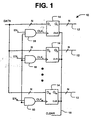
- a multiplexer 10 includes M diode-based latches 14, where integer M>1. Inputs (D 1 to D M ) of the latches 14 are connected in parallel so that each latch 14 receives the same N-bit word (DATA). Each latch 14 has an output line 12 that is N-bits wide, where integer N>1. The multiplexer 10 can receive an N-bit word (DATA) and forward that N-bit word (DATA) to any one of M output lines 12.
- Clock signals (CLK 1 , CLK 2 , ..., CLK M ) are supplied to the clock inputs of the latches 14. For instance, the clock signal CLK 1 is supplied to the first latch 14. When the clock signal CLK 1 is high, the first latch 14 stores the data word (DATA). When the clock signal CLK 1 goes low, the stored data is made available on the output line 12 of the first latch 14.
- a reference clock (CLK) and enable signals (EN 1 , EN 2 , ..., EN M ) are generated by a signal generator (not shown in Figure 1). Each enable signal (EN 1 , EN 2 , ..., EN M ) corresponds to a latch 14.
- the multiplexer 10 further includes gates 16 for generating the clock signals (CLK 1 , CLK 2 , ..., CLK M ) from the reference clock (CLK) and the enable signals (EN 1 , EN 2 , ..., EN M ). For instance, when the reference clock (CLK) and the first enable signal (EN 1 ) are high, the first latch 14 stores the data word (DATA).
- the gates 16 may be based on ECL technology or another technology that does not use transistors.
- the multiplexer 10 also Includes a line 18 for clearing data stored in the latches 14.
- a clear data signal (CLEAR) is generated by the signal generator and supplied to the clear data line 18.
- the multiplexer shown in Figure 1 provides about an M:1 reduction in input lines.
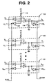
- FIG. 2 shows a diode-based latch 14 in greater detail.
- the latch 14 includes N stages 110, each stage 110 having a data input (D n ), a power supply input (P n ), and a data output (Q n ), where 0 ⁇ n ⁇ (N-1).
- the data input (D 0 ) of the first stage 110 receives the first bit of the data word (DATA)
- the data input (D 1 ) of the second stage receives the 2 nd bit of the data word (DATA)
- the data input (D N-1 ) of the N th stage receives the N th bit of the data word (DATA).
- the N data outputs (Q 0 to Q N-1 ) of the N stages 110 are connected to an N-bit data line 12.
- a pull-up resistor 112 is connected between the power supply input (P n ) and a voltage source (+V).
- Each stage 110 Includes a charge storage device (e.g., a capacitor) 114 coupled to the data output (Q n ); a first diode 116 coupled between the data input (D n ) and the power supply input (P n ); and a second diode 118 coupled between the power supply input (P n ) and the data output (Q n ).
- the cathode of the first diode 116 is connected to the data input (D n ), and the anode of the first diode 116 is connected to the power supply input (P n ).
- the cathode of the second diode 118 is connected to the data output (Q n ), and the anode of the second diode 118 is connected to the power supply input (P n ).
- Each stage 110 further has a clock input (C n ) and a third diode 120 connected between the clock input (C n ) and the power supply input (P n ).
- the clock inputs (C 0 to C N-1 ) of the stages 110 are tied together to receive the same clock signal (e.g., CLK 1 ).
- Each stage 110 also has a clear data input (CD n ) and a fourth diode 122 connected between the clear data input (CD n ) and the data output (Qn).
- the clear data inputs (CD 0 to CD N-1 ) of the stages 110 are tied together to receive the same clear data signal (CLEAR).
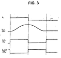
- the clock signal (CLK 1 ) is asserted and the clear data signal (CLEAR) is de-asserted.
- the third and fourth diodes 120 and 122 become reverse biased. If the data word bit (D 1 ) is high, the first diode 116 becomes reverse biased and the second diode 118 becomes forward biased. Current flows through the pull-up resistor 112 and the second diode 118, and charges the capacitor 114. Capacitor voltage (V CAP ) rises.
- V CAP high capacitor voltage
- V CAP Capacitor voltage
- the clock signal (CLK 1 ) is asserted and the clear data signal (CLEAR) is de-asserted.
- CLK 1 the clock signal
- CLAR clear data signal
- the third and fourth diodes 120 and 122 become reverse biased. If the data word bit (D 1 ) is low, the first diode 116 becomes forward biased. Current flows through the first diode 116, and the capacitor 114 is not charged. Therefore, capacitor voltage (Vcap) does not rise.
- Vcap low capacitor voltage
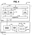
- Figure 4 shows a diode-based OTP memory device 210.
- One or more memory levels 212 are stacked on a silicon substrate 214.
- Each level 212 Includes M sub-arrays 216.
- Each sub-array 216 is described in greater detail below.
- Data is read out from sub-arrays 216 on data lines 218.
- the data lines 218 are supplied to a data multiplexer 220 (which may have the same construction as the multiplexer 10 shown in Figure 1).
- An output of the data multiplexer 220 is supplied to a signal conditioning circuit 222 on the substrate 214.
- Addresses are decoded by row and column drivers 224, and the decoded addresses are multiplexed to the appropriate address lines 226 by an address multiplexer 228 (which may have the same construction as the multiplexer 10 shown in Figure 1).
- the row and column driver 224 are also on the substrate 214
- the enable signals (EN 1 , EN 2 , ..., EN M ), the reference clock (CLK) and the clear data signal (CLEAR) are generated by a signal generator 230 on the substrate 214. These timing signals may be generated by decoding the addresses.
- a sub-array 216 includes a cross point resistive array 310 of OTP memory elements 312, word lines 314 extending along rows of the memory elements 312, and bit lines 316 extending along columns of the memory elements 312. There may be one word line 314 for each row of the memory elements 312 and one bit line 316 for each column of memory elements 312. Each memory element 312 is located at a cross point of a word line 314 and a bit line 316.
- An OTP row decoder 318 selects the word lines 314 by decoding addresses supplied to row address lines 226 by the address multiplexer 228.
- the row decoder 318 includes a plurality of OTP address elements 320. Each address element 320 of the row decoder 318 is at a cross point of a word line 314 and a row address line 226.
- An OTP column decoder 322 selects the column lines 316 by decoding addresses supplied to column address lines 226 by the address multiplexer 228.
- the column decoder 322 includes a plurality of OTP address elements 320. Each address element 320 of the column decoder 322 is at a cross point of a bit line 316 and a column address line 226.
- Data may be written to the device 210 by supplying an address to the row/column drivers 224 and the signal generator 230.
- the signal generator 230 decodes the address and causes the address multiplexer 228 to select a sub-array.
- the row/column drivers 224 decode the address and send the decoded address to the address multiplexer 228 and, therefore, to the selected sub-array.
- the address logic of the selected sub-array receives the decoded address (via the address lines 226) and selects word and bit lines 314 and 316.
- a write current flows through the selected word and bit lines 314 and 316 and, therefore, flows through a memory element 312 at the cross point of the selected word and bit lines 314 and 316. Magnitude of the write current is sufficient to change the resistance state of the selected memory element 312.
- the resistance state of a memory element 312 may be sensed by supplying an address to the row/column drivers 224.
- the address multiplexer 228 sends a decoded address to a selected a sub-array.
- word and bit lines 314 and 316 are selected.
- a sense current flows through the selected word and bit lines 314 and 316 and, therefore, flows through a memory element 312 at the cross point of the selected word and bit lines 314 and 316.
- Magnitude of the sense current indicates the resistance state of the selected memory element 216.
- the sense current is converted to a digital value, and the data multiplexer sends the digital value to the signal conditioning circuit 222 on the substrate 214. All data out from a sub-array is effectively wired together, however, only the memory bit which corresponds to the selected address is enabled.
Description
- The present invention relates to multiplexers. The present invention also relates to one-time programmable (OTP) solid state memory.
- Portable devices such as PDAs, handheld computers, digital cameras and digital music players include memory for storing data, digital images and MP3 files. Different types of memory are available for these portable devices. Conventional memory types include flash memory, mini-hard drives, mini-compact discs, and magnetic tape. However, each of these memory types has one or more of the following limitations: large physical size, low storage capacity, relatively high cost, poor robustness, slow access time and high power consumption.
- Solid state diode-based OTP memory is disclosed in co-pending European patent application 1265287. Compared to the conventional memory, the diode-based memory has a high shock tolerance, low power consumption, fast access time, moderate transfer rate and good storage capacity. The diode-based memory can fit into a standard portable interface (e.g., PCMCIA, CF) of a portable device.
- Solid state diode-based OTP memory devices can include large numbers of data and address lines. Multiplexers may be used to reduce the number of data and address lines to a device.
- The multiplexers may be based on transistor logic such as TTL. However, manufacturing the layers required for transistors in a diode-based OTP device would increase the cost and complexity of the device.
- It would be desirable to avoid the use of transistors in multiplexers of diode-based OTP memory devices.
- The article DIODE MULTIPLEXER IN THE MULTI-GBIT/S RANGE, ELECTRONICS LETTERS,
Vol 14. No. 3, pages 62-64 discloses a multiplexer including clocked circuits employing diodes. - According to an aspect of the present invention there is provided a multiplexer comprising M latches, each latch having N stages, where integer M>1 and integer N>1, and logic means for enabling at least one of the latches at a time, each stage having a data input (Dn), a power supply input (Pn), and a data output (Qn), each stage including a charge storage device coupled to the data output (Qn), a first diode coupled between the data input (Dn) and the power supply input (Pn) and a second diode coupled between the power supply input (Pn) and the data output (Qn), and each stage having a clock input (Cn) connected to said logic means.
- Other aspects and advantages of the present invention will become apparent from the following detailed description, taken in conjunction with the accompanying drawings, illustrating by way of example the principles of the present invention.
- Figure 1 is an illustration of a multiplexer according to the present invention.
- Figure 2 is an illustration of a latch for the multiplexer.
- Figure 3 is a timing diagram for the multiplexer.
- Figure 4 is an illustration of a diode-based memory device including sub-arrays and multiplexers according to the present invention.
- Figure 5 is an illustration of a sub-array.
- Referring to Figure 1, a
multiplexer 10 includes M diode-basedlatches 14, where integer M>1. Inputs (D1 to DM) of thelatches 14 are connected in parallel so that eachlatch 14 receives the same N-bit word (DATA). Eachlatch 14 has anoutput line 12 that is N-bits wide, where integer N>1. Themultiplexer 10 can receive an N-bit word (DATA) and forward that N-bit word (DATA) to any one ofM output lines 12. - Clock signals (CLK1, CLK2, ..., CLKM) are supplied to the clock inputs of the
latches 14. For instance, the clock signal CLK1 is supplied to thefirst latch 14. When the clock signal CLK1 is high, thefirst latch 14 stores the data word (DATA). When the clock signal CLK1 goes low, the stored data is made available on theoutput line 12 of thefirst latch 14. - A reference clock (CLK) and enable signals (EN1, EN2, ..., ENM) are generated by a signal generator (not shown in Figure 1). Each enable signal (EN1, EN2, ..., ENM) corresponds to a
latch 14. Themultiplexer 10 further includesgates 16 for generating the clock signals (CLK1, CLK2, ..., CLKM) from the reference clock (CLK) and the enable signals (EN1, EN2, ..., ENM). For instance, when the reference clock (CLK) and the first enable signal (EN1) are high, thefirst latch 14 stores the data word (DATA). Thegates 16 may be based on ECL technology or another technology that does not use transistors. - The
multiplexer 10 also Includes aline 18 for clearing data stored in thelatches 14. A clear data signal (CLEAR) is generated by the signal generator and supplied to theclear data line 18. - The multiplexer shown in Figure 1 provides about an M:1 reduction in input lines. Thus a multiplexer having M=32 latches provides an almost 32:1 reduction in input lines.
- Figure 2 shows a diode-based
latch 14 in greater detail. Thelatch 14 includesN stages 110, eachstage 110 having a data input (Dn), a power supply input (Pn), and a data output (Qn), where 0≤n≤(N-1). The data input (D0) of thefirst stage 110 receives the first bit of the data word (DATA), the data input (D1) of the second stage receives the 2nd bit of the data word (DATA), and the data input (DN-1) of the Nth stage receives the Nth bit of the data word (DATA). The N data outputs (Q0 to QN-1) of theN stages 110 are connected to an N-bit data line 12. For eachstage 110, a pull-up resistor 112 is connected between the power supply input (Pn) and a voltage source (+V). - Each
stage 110 Includes a charge storage device (e.g., a capacitor) 114 coupled to the data output (Qn); afirst diode 116 coupled between the data input (Dn) and the power supply input (Pn); and asecond diode 118 coupled between the power supply input (Pn) and the data output (Qn). The cathode of thefirst diode 116 is connected to the data input (Dn), and the anode of thefirst diode 116 is connected to the power supply input (Pn). The cathode of thesecond diode 118 is connected to the data output (Qn), and the anode of thesecond diode 118 is connected to the power supply input (Pn). - Each
stage 110 further has a clock input (Cn) and athird diode 120 connected between the clock input (Cn) and the power supply input (Pn). The clock inputs (C0 to CN-1) of thestages 110 are tied together to receive the same clock signal (e.g., CLK1). - Each
stage 110 also has a clear data input (CDn) and afourth diode 122 connected between the clear data input (CDn) and the data output (Qn). The clear data inputs (CD0 to CDN-1) of thestages 110 are tied together to receive the same clear data signal (CLEAR). - Additional reference is made to Figure 3. Operation of the
second stage 110 will now be described by the following example. Initial conditions are as follows. The clock signal is de-asserted and the clear signal is asserted. The third andfourth diodes third diode 120, and thecapacitor 114 is discharged through thefourth diode 122. - At the beginning of the operation, the clock signal (CLK1) is asserted and the clear data signal (CLEAR) is de-asserted. The third and
fourth diodes first diode 116 becomes reverse biased and thesecond diode 118 becomes forward biased. Current flows through the pull-up resistor 112 and thesecond diode 118, and charges thecapacitor 114. Capacitor voltage (VCAP) rises. - Data is read out at the trailing edge of the clock signal (CLK1). A high capacitor voltage (VCAP) is read at the data output (Q1). This high voltage corresponds to the high data state.
- After data has been read out, the clear data signal (CLEAR) is re-asserted. Consequently, the third and
fourth diodes third diode 120, and thecapacitor 114 is discharged through thefourth diode 122. Capacitor voltage (VCAP) falls. - At the beginning of the next clock cycle, the clock signal (CLK1) is asserted and the clear data signal (CLEAR) is de-asserted. The third and
fourth diodes first diode 116 becomes forward biased. Current flows through thefirst diode 116, and thecapacitor 114 is not charged. Therefore, capacitor voltage (Vcap) does not rise. - Data is read out at the trailing edge of the clock signal (CLK1). A low capacitor voltage (Vcap) at the data output (Q1) corresponds to the low data state.
- Figure 4 shows a diode-based
OTP memory device 210. One ormore memory levels 212 are stacked on asilicon substrate 214. Eachlevel 212 IncludesM sub-arrays 216. Each sub-array 216 is described in greater detail below. Data is read out from sub-arrays 216 ondata lines 218. The data lines 218 are supplied to a data multiplexer 220 (which may have the same construction as themultiplexer 10 shown in Figure 1). An output of thedata multiplexer 220 is supplied to asignal conditioning circuit 222 on thesubstrate 214. - Addresses are decoded by row and
column drivers 224, and the decoded addresses are multiplexed to theappropriate address lines 226 by an address multiplexer 228 (which may have the same construction as themultiplexer 10 shown in Figure 1). The row andcolumn driver 224 are also on thesubstrate 214 - The enable signals (EN1, EN2, ..., ENM), the reference clock (CLK) and the clear data signal (CLEAR) are generated by a
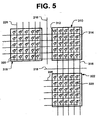
signal generator 230 on thesubstrate 214. These timing signals may be generated by decoding the addresses. - Reference is now made to Figure 5. A sub-array 216 includes a cross point
resistive array 310 ofOTP memory elements 312,word lines 314 extending along rows of thememory elements 312, and bitlines 316 extending along columns of thememory elements 312. There may be oneword line 314 for each row of thememory elements 312 and onebit line 316 for each column ofmemory elements 312. Eachmemory element 312 is located at a cross point of aword line 314 and abit line 316. - An
OTP row decoder 318 selects the word lines 314 by decoding addresses supplied to rowaddress lines 226 by theaddress multiplexer 228. Therow decoder 318 includes a plurality of OTP addresselements 320. Eachaddress element 320 of therow decoder 318 is at a cross point of aword line 314 and arow address line 226. - An
OTP column decoder 322 selects thecolumn lines 316 by decoding addresses supplied tocolumn address lines 226 by theaddress multiplexer 228. Thecolumn decoder 322 includes a plurality of OTP addresselements 320. Eachaddress element 320 of thecolumn decoder 322 is at a cross point of abit line 316 and acolumn address line 226. - The
memory elements 312 and theaddress elements 320 both include diodes. - Data may be written to the
device 210 by supplying an address to the row/column drivers 224 and thesignal generator 230. Thesignal generator 230 decodes the address and causes theaddress multiplexer 228 to select a sub-array. The row/column drivers 224 decode the address and send the decoded address to theaddress multiplexer 228 and, therefore, to the selected sub-array. The address logic of the selected sub-array receives the decoded address (via the address lines 226) and selects word andbit lines bit lines memory element 312 at the cross point of the selected word andbit lines memory element 312. - The resistance state of a
memory element 312 may be sensed by supplying an address to the row/column drivers 224. Theaddress multiplexer 228 sends a decoded address to a selected a sub-array. In response to the decoded address, word andbit lines bit lines memory element 312 at the cross point of the selected word andbit lines memory element 216. The sense current is converted to a digital value, and the data multiplexer sends the digital value to thesignal conditioning circuit 222 on thesubstrate 214. All data out from a sub-array is effectively wired together, however, only the memory bit which corresponds to the selected address is enabled. - The present invention is not limited to the specific embodiments described and illustrated above. Instead, the present invention is construed according to the claims that follow.
Claims (6)
- A multiplexer (10) comprising M latches (14), each latch (14) having N stages (110), where integer M>1 and integer N>1, and logic means (16) for enabling at least one of the latches (14) at a time, each stage having a data input (Dn), a power supply input (Pn), and a data output (Qn), each stage (110) including a charge storage device (114) coupled to the data output (Qn), a first diode (116) coupled between the data input (Dn)and the power supply input (Pn), and a second diode (118) coupled between then power supply input (Pn) and the data output (Qn), and each stage having a clock input (Cn) connected to said logic means (16).
- The multiplexer (10) of claim 1, wherein each latch (14) has an N-bit wide input formed by the data inputs (Dn) of its N stages (110), and wherein each latch (14) has an N-bit wide output (12) formed by the data outputs . (Qn) of its N stages (110).
- The multiplexer (10) of claim 1 or 2, each stage (110) further having a third diode (120) connected between the clock input (Cn) and the power supply input (Pn).
- The multiplexer of any preceding claim, wherein the clock inputs (Cn) of the stages (110) are tied together.
- The multiplexer (10) of any preceding claim, each stage further having a clear data input (CDn), and a third diode (122) connected between the clear data input (CDn) and the data output (Qn), whrein the clear data inputs (CDn) of the stages (110) are tied together.
- The multiplexer (10) of any preceding claim, wherein input data determines whether the first diode (116) is forward biased or reverse biased; whereby the latch (14) is set to a first logic state if the first diode (116) is forward biased, and whereby the latch (14) is set to a second logic state if the first diode (116) is reverse biased.
Applications Claiming Priority (2)
| Application Number | Priority Date | Filing Date | Title |
|---|---|---|---|
| US976744 | 2001-10-13 | ||
| US09/976,744 US6614697B2 (en) | 2001-10-13 | 2001-10-13 | Diode-based multiplexer |
Publications (2)
| Publication Number | Publication Date |
|---|---|
| EP1303044A1 EP1303044A1 (en) | 2003-04-16 |
| EP1303044B1 true EP1303044B1 (en) | 2006-05-03 |
Family
ID=25524408
Family Applications (1)
| Application Number | Title | Priority Date | Filing Date |
|---|---|---|---|
| EP02256961A Expired - Lifetime EP1303044B1 (en) | 2001-10-13 | 2002-10-08 | Diode-based multiplexer |
Country Status (7)
| Country | Link |
|---|---|
| US (1) | US6614697B2 (en) |
| EP (1) | EP1303044B1 (en) |
| JP (1) | JP3961392B2 (en) |
| KR (1) | KR20030031423A (en) |
| CN (1) | CN1412779A (en) |
| DE (1) | DE60211093T2 (en) |
| TW (1) | TWI240281B (en) |
Families Citing this family (3)
| Publication number | Priority date | Publication date | Assignee | Title |
|---|---|---|---|---|
| EP1157466A1 (en) * | 1999-12-21 | 2001-11-28 | Koninklijke Philips Electronics N.V. | Diode multiplexer circuit and electronic device incorporating the same |
| US7747415B1 (en) * | 2005-12-22 | 2010-06-29 | Microstrain, Inc. | Sensor powered event logger |
| TWI340911B (en) * | 2007-04-13 | 2011-04-21 | Generalplus Technology Inc | Capacitance touch sensor |
Family Cites Families (6)
| Publication number | Priority date | Publication date | Assignee | Title |
|---|---|---|---|---|
| US5900767A (en) | 1995-06-24 | 1999-05-04 | U.S. Philips Corporation | Electronic devices comprising an array |
| GB9524560D0 (en) * | 1995-12-01 | 1996-01-31 | Philips Electronics Nv | Multiplexer circuit |
| GB9614480D0 (en) * | 1995-12-01 | 1996-09-04 | Philips Electronics Nv | Multiplexer circuit |
| GB9600543D0 (en) * | 1996-01-11 | 1996-03-13 | Philips Electronics Nv | Electronic devices comprising an array |
| US6199140B1 (en) * | 1997-10-30 | 2001-03-06 | Netlogic Microsystems, Inc. | Multiport content addressable memory device and timing signals |
| EP1157466A1 (en) * | 1999-12-21 | 2001-11-28 | Koninklijke Philips Electronics N.V. | Diode multiplexer circuit and electronic device incorporating the same |
-
2001
- 2001-10-13 US US09/976,744 patent/US6614697B2/en not_active Expired - Lifetime
-
2002
- 2002-08-29 TW TW091119704A patent/TWI240281B/en not_active IP Right Cessation
- 2002-10-08 DE DE60211093T patent/DE60211093T2/en not_active Expired - Lifetime
- 2002-10-08 EP EP02256961A patent/EP1303044B1/en not_active Expired - Lifetime
- 2002-10-11 CN CN02143600A patent/CN1412779A/en active Pending
- 2002-10-11 JP JP2002298312A patent/JP3961392B2/en not_active Expired - Fee Related
- 2002-10-12 KR KR1020020062230A patent/KR20030031423A/en not_active Application Discontinuation
Also Published As
| Publication number | Publication date |
|---|---|
| JP2003142994A (en) | 2003-05-16 |
| DE60211093D1 (en) | 2006-06-08 |
| TWI240281B (en) | 2005-09-21 |
| US20030072184A1 (en) | 2003-04-17 |
| DE60211093T2 (en) | 2007-02-01 |
| CN1412779A (en) | 2003-04-23 |
| EP1303044A1 (en) | 2003-04-16 |
| US6614697B2 (en) | 2003-09-02 |
| KR20030031423A (en) | 2003-04-21 |
| JP3961392B2 (en) | 2007-08-22 |
Similar Documents
| Publication | Publication Date | Title |
|---|---|---|
| US6618295B2 (en) | Method and apparatus for biasing selected and unselected array lines when writing a memory array | |
| JP4148507B2 (en) | Field programmable gate array | |
| US6882570B2 (en) | Power detecting circuit and method for stable power-on reading of flash memory device using the same | |
| JP5059199B2 (en) | CMOS decoding circuit | |
| KR102515463B1 (en) | Nonvolatile memory apparatus, and read and write method thereof | |
| JP5099674B2 (en) | Semiconductor integrated circuit | |
| CN111435294B (en) | Random code generator | |
| JP4060330B2 (en) | Semiconductor memory device and bit line selection method for semiconductor memory device | |
| EP1303044B1 (en) | Diode-based multiplexer | |
| US8526217B2 (en) | Low-complexity electronic circuit and methods of forming the same | |
| US9659620B2 (en) | Memory device with self-boosted mechanism | |
| US20120002487A1 (en) | Nonvolatile memory apparatus and method for processing configuration information thereof | |
| WO2007015097A1 (en) | Memory bitcell and method of using the same | |
| JP5197704B2 (en) | Semiconductor device | |
| US8154920B2 (en) | Method of reading data and method of inputting and outputting data in non-volatile memory device | |
| US7596029B2 (en) | Flash memory device including unified oscillation circuit and method of operating the device | |
| US6826112B2 (en) | Low power logic gate | |
| US11049549B2 (en) | Decoder structure including array of decoder cells organized into different rows | |
| US20230018420A1 (en) | Sram with fast, controlled peak current, power efficient array reset, and data corruption modes for secure applications | |
| US20100271890A1 (en) | Data i/o control signal generating circuit in a semiconductor memory apparatus | |
| US20120163114A1 (en) | NAND logic word line selection | |
| CN115938436A (en) | Storage circuit and storage array | |
| JPH0247922A (en) | Programmable logic element |
Legal Events
| Date | Code | Title | Description |
|---|---|---|---|
| PUAI | Public reference made under article 153(3) epc to a published international application that has entered the european phase |
Free format text: ORIGINAL CODE: 0009012 |
|
| AK | Designated contracting states |
Designated state(s): AT BE BG CH CY CZ DE DK EE ES FI FR GB GR IE IT LI LU MC NL PT SE SK TR |
|
| AX | Request for extension of the european patent |
Extension state: AL LT LV MK RO SI |
|
| 17P | Request for examination filed |
Effective date: 20031015 |
|
| AKX | Designation fees paid |
Designated state(s): DE GB |
|
| 17Q | First examination report despatched |
Effective date: 20050303 |
|
| GRAP | Despatch of communication of intention to grant a patent |
Free format text: ORIGINAL CODE: EPIDOSNIGR1 |
|
| GRAS | Grant fee paid |
Free format text: ORIGINAL CODE: EPIDOSNIGR3 |
|
| GRAA | (expected) grant |
Free format text: ORIGINAL CODE: 0009210 |
|
| AK | Designated contracting states |
Kind code of ref document: B1 Designated state(s): DE GB |
|
| REG | Reference to a national code |
Ref country code: GB Ref legal event code: FG4D |
|
| REF | Corresponds to: |
Ref document number: 60211093 Country of ref document: DE Date of ref document: 20060608 Kind code of ref document: P |
|
| PLBE | No opposition filed within time limit |
Free format text: ORIGINAL CODE: 0009261 |
|
| STAA | Information on the status of an ep patent application or granted ep patent |
Free format text: STATUS: NO OPPOSITION FILED WITHIN TIME LIMIT |
|
| 26N | No opposition filed |
Effective date: 20070206 |
|
| REG | Reference to a national code |
Ref country code: GB Ref legal event code: 732E Free format text: REGISTERED BETWEEN 20110203 AND 20110209 |
|
| REG | Reference to a national code |
Ref country code: DE Ref legal event code: R081 Ref document number: 60211093 Country of ref document: DE Owner name: SAMSUNG ELECTRONICS CO., LTD., SUWON-SI, KR Free format text: FORMER OWNER: HEWLETT-PACKARD DEVELOPMENT COMPANY, L.P., HOUSTON, TEX., US Effective date: 20110426 |
|
| PGFP | Annual fee paid to national office [announced via postgrant information from national office to epo] |
Ref country code: GB Payment date: 20210831 Year of fee payment: 20 |
|
| PGFP | Annual fee paid to national office [announced via postgrant information from national office to epo] |
Ref country code: DE Payment date: 20210831 Year of fee payment: 20 |
|
| REG | Reference to a national code |
Ref country code: DE Ref legal event code: R071 Ref document number: 60211093 Country of ref document: DE |
|
| REG | Reference to a national code |
Ref country code: GB Ref legal event code: PE20 Expiry date: 20221007 |
|
| PG25 | Lapsed in a contracting state [announced via postgrant information from national office to epo] |
Ref country code: GB Free format text: LAPSE BECAUSE OF EXPIRATION OF PROTECTION Effective date: 20221007 |
|
| P01 | Opt-out of the competence of the unified patent court (upc) registered |
Effective date: 20230524 |