EP1302981A2 - Method of manufacturing semiconductor device having silicon carbide film - Google Patents
Method of manufacturing semiconductor device having silicon carbide film Download PDFInfo
- Publication number
- EP1302981A2 EP1302981A2 EP02002111A EP02002111A EP1302981A2 EP 1302981 A2 EP1302981 A2 EP 1302981A2 EP 02002111 A EP02002111 A EP 02002111A EP 02002111 A EP02002111 A EP 02002111A EP 1302981 A2 EP1302981 A2 EP 1302981A2
- Authority
- EP
- European Patent Office
- Prior art keywords
- film
- etching
- forming
- resist
- substrate
- Prior art date
- Legal status (The legal status is an assumption and is not a legal conclusion. Google has not performed a legal analysis and makes no representation as to the accuracy of the status listed.)
- Withdrawn
Links
Images







Classifications
-
- H—ELECTRICITY
- H10—SEMICONDUCTOR DEVICES; ELECTRIC SOLID-STATE DEVICES NOT OTHERWISE PROVIDED FOR
- H10P—GENERIC PROCESSES OR APPARATUS FOR THE MANUFACTURE OR TREATMENT OF DEVICES COVERED BY CLASS H10
- H10P14/00—Formation of materials, e.g. in the shape of layers or pillars
- H10P14/60—Formation of materials, e.g. in the shape of layers or pillars of insulating materials
- H10P14/66—Formation of materials, e.g. in the shape of layers or pillars of insulating materials characterised by the type of materials
- H10P14/662—Laminate layers, e.g. stacks of alternating high-k metal oxides
-
- H—ELECTRICITY
- H10—SEMICONDUCTOR DEVICES; ELECTRIC SOLID-STATE DEVICES NOT OTHERWISE PROVIDED FOR
- H10W—GENERIC PACKAGES, INTERCONNECTIONS, CONNECTORS OR OTHER CONSTRUCTIONAL DETAILS OF DEVICES COVERED BY CLASS H10
- H10W20/00—Interconnections in chips, wafers or substrates
- H10W20/01—Manufacture or treatment
-
- H—ELECTRICITY
- H10—SEMICONDUCTOR DEVICES; ELECTRIC SOLID-STATE DEVICES NOT OTHERWISE PROVIDED FOR
- H10P—GENERIC PROCESSES OR APPARATUS FOR THE MANUFACTURE OR TREATMENT OF DEVICES COVERED BY CLASS H10
- H10P14/00—Formation of materials, e.g. in the shape of layers or pillars
- H10P14/60—Formation of materials, e.g. in the shape of layers or pillars of insulating materials
- H10P14/63—Formation of materials, e.g. in the shape of layers or pillars of insulating materials characterised by the formation processes
- H10P14/6326—Deposition processes
- H10P14/6328—Deposition from the gas or vapour phase
- H10P14/6334—Deposition from the gas or vapour phase using decomposition or reaction of gaseous or vapour phase compounds, i.e. chemical vapour deposition
-
- H—ELECTRICITY
- H10—SEMICONDUCTOR DEVICES; ELECTRIC SOLID-STATE DEVICES NOT OTHERWISE PROVIDED FOR
- H10P—GENERIC PROCESSES OR APPARATUS FOR THE MANUFACTURE OR TREATMENT OF DEVICES COVERED BY CLASS H10
- H10P14/00—Formation of materials, e.g. in the shape of layers or pillars
- H10P14/60—Formation of materials, e.g. in the shape of layers or pillars of insulating materials
- H10P14/66—Formation of materials, e.g. in the shape of layers or pillars of insulating materials characterised by the type of materials
- H10P14/665—Porous materials
-
- H—ELECTRICITY
- H10—SEMICONDUCTOR DEVICES; ELECTRIC SOLID-STATE DEVICES NOT OTHERWISE PROVIDED FOR
- H10P—GENERIC PROCESSES OR APPARATUS FOR THE MANUFACTURE OR TREATMENT OF DEVICES COVERED BY CLASS H10
- H10P14/00—Formation of materials, e.g. in the shape of layers or pillars
- H10P14/60—Formation of materials, e.g. in the shape of layers or pillars of insulating materials
- H10P14/66—Formation of materials, e.g. in the shape of layers or pillars of insulating materials characterised by the type of materials
- H10P14/668—Formation of materials, e.g. in the shape of layers or pillars of insulating materials characterised by the type of materials the materials being characterised by the deposition precursor materials
- H10P14/6681—Formation of materials, e.g. in the shape of layers or pillars of insulating materials characterised by the type of materials the materials being characterised by the deposition precursor materials the precursor containing a compound comprising Si
- H10P14/6682—Formation of materials, e.g. in the shape of layers or pillars of insulating materials characterised by the type of materials the materials being characterised by the deposition precursor materials the precursor containing a compound comprising Si the compound being a silane, e.g. disilane, methylsilane or chlorosilane
-
- H—ELECTRICITY
- H10—SEMICONDUCTOR DEVICES; ELECTRIC SOLID-STATE DEVICES NOT OTHERWISE PROVIDED FOR
- H10P—GENERIC PROCESSES OR APPARATUS FOR THE MANUFACTURE OR TREATMENT OF DEVICES COVERED BY CLASS H10
- H10P14/00—Formation of materials, e.g. in the shape of layers or pillars
- H10P14/60—Formation of materials, e.g. in the shape of layers or pillars of insulating materials
- H10P14/69—Inorganic materials
- H10P14/6903—Inorganic materials containing silicon
- H10P14/6905—Inorganic materials containing silicon being a silicon carbide or silicon carbonitride and not containing oxygen, e.g. SiC or SiC:H
-
- H—ELECTRICITY
- H10—SEMICONDUCTOR DEVICES; ELECTRIC SOLID-STATE DEVICES NOT OTHERWISE PROVIDED FOR
- H10P—GENERIC PROCESSES OR APPARATUS FOR THE MANUFACTURE OR TREATMENT OF DEVICES COVERED BY CLASS H10
- H10P14/00—Formation of materials, e.g. in the shape of layers or pillars
- H10P14/60—Formation of materials, e.g. in the shape of layers or pillars of insulating materials
- H10P14/69—Inorganic materials
- H10P14/692—Inorganic materials composed of oxides, glassy oxides or oxide-based glasses
- H10P14/6921—Inorganic materials composed of oxides, glassy oxides or oxide-based glasses containing silicon
- H10P14/69215—Inorganic materials composed of oxides, glassy oxides or oxide-based glasses containing silicon the material being a silicon oxide, e.g. SiO2
-
- H—ELECTRICITY
- H10—SEMICONDUCTOR DEVICES; ELECTRIC SOLID-STATE DEVICES NOT OTHERWISE PROVIDED FOR
- H10P—GENERIC PROCESSES OR APPARATUS FOR THE MANUFACTURE OR TREATMENT OF DEVICES COVERED BY CLASS H10
- H10P14/00—Formation of materials, e.g. in the shape of layers or pillars
- H10P14/60—Formation of materials, e.g. in the shape of layers or pillars of insulating materials
- H10P14/69—Inorganic materials
- H10P14/692—Inorganic materials composed of oxides, glassy oxides or oxide-based glasses
- H10P14/6921—Inorganic materials composed of oxides, glassy oxides or oxide-based glasses containing silicon
- H10P14/6922—Inorganic materials composed of oxides, glassy oxides or oxide-based glasses containing silicon the material containing Si, O and at least one of H, N, C, F or other non-metal elements, e.g. SiOC, SiOC:H or SiONC
- H10P14/6923—Inorganic materials composed of oxides, glassy oxides or oxide-based glasses containing silicon the material containing Si, O and at least one of H, N, C, F or other non-metal elements, e.g. SiOC, SiOC:H or SiONC the material being boron or phosphorus doped silicon oxides, e.g. BPSG, BSG or PSG
-
- H—ELECTRICITY
- H10—SEMICONDUCTOR DEVICES; ELECTRIC SOLID-STATE DEVICES NOT OTHERWISE PROVIDED FOR
- H10P—GENERIC PROCESSES OR APPARATUS FOR THE MANUFACTURE OR TREATMENT OF DEVICES COVERED BY CLASS H10
- H10P14/00—Formation of materials, e.g. in the shape of layers or pillars
- H10P14/60—Formation of materials, e.g. in the shape of layers or pillars of insulating materials
- H10P14/69—Inorganic materials
- H10P14/692—Inorganic materials composed of oxides, glassy oxides or oxide-based glasses
- H10P14/6921—Inorganic materials composed of oxides, glassy oxides or oxide-based glasses containing silicon
- H10P14/6922—Inorganic materials composed of oxides, glassy oxides or oxide-based glasses containing silicon the material containing Si, O and at least one of H, N, C, F or other non-metal elements, e.g. SiOC, SiOC:H or SiONC
- H10P14/6925—Inorganic materials composed of oxides, glassy oxides or oxide-based glasses containing silicon the material containing Si, O and at least one of H, N, C, F or other non-metal elements, e.g. SiOC, SiOC:H or SiONC the material comprising hydrogen silsesquioxane, e.g. HSQ
-
- H—ELECTRICITY
- H10—SEMICONDUCTOR DEVICES; ELECTRIC SOLID-STATE DEVICES NOT OTHERWISE PROVIDED FOR
- H10P—GENERIC PROCESSES OR APPARATUS FOR THE MANUFACTURE OR TREATMENT OF DEVICES COVERED BY CLASS H10
- H10P50/00—Etching of wafers, substrates or parts of devices
- H10P50/20—Dry etching; Plasma etching; Reactive-ion etching
- H10P50/28—Dry etching; Plasma etching; Reactive-ion etching of insulating materials
- H10P50/282—Dry etching; Plasma etching; Reactive-ion etching of insulating materials of inorganic materials
- H10P50/283—Dry etching; Plasma etching; Reactive-ion etching of insulating materials of inorganic materials by chemical means
-
- H—ELECTRICITY
- H10—SEMICONDUCTOR DEVICES; ELECTRIC SOLID-STATE DEVICES NOT OTHERWISE PROVIDED FOR
- H10P—GENERIC PROCESSES OR APPARATUS FOR THE MANUFACTURE OR TREATMENT OF DEVICES COVERED BY CLASS H10
- H10P50/00—Etching of wafers, substrates or parts of devices
- H10P50/73—Etching of wafers, substrates or parts of devices using masks for insulating materials
-
- H—ELECTRICITY
- H10—SEMICONDUCTOR DEVICES; ELECTRIC SOLID-STATE DEVICES NOT OTHERWISE PROVIDED FOR
- H10W—GENERIC PACKAGES, INTERCONNECTIONS, CONNECTORS OR OTHER CONSTRUCTIONAL DETAILS OF DEVICES COVERED BY CLASS H10
- H10W20/00—Interconnections in chips, wafers or substrates
- H10W20/01—Manufacture or treatment
- H10W20/071—Manufacture or treatment of dielectric parts thereof
-
- H—ELECTRICITY
- H10—SEMICONDUCTOR DEVICES; ELECTRIC SOLID-STATE DEVICES NOT OTHERWISE PROVIDED FOR
- H10W—GENERIC PACKAGES, INTERCONNECTIONS, CONNECTORS OR OTHER CONSTRUCTIONAL DETAILS OF DEVICES COVERED BY CLASS H10
- H10W20/00—Interconnections in chips, wafers or substrates
- H10W20/01—Manufacture or treatment
- H10W20/071—Manufacture or treatment of dielectric parts thereof
- H10W20/081—Manufacture or treatment of dielectric parts thereof by forming openings in the dielectric parts
-
- H—ELECTRICITY
- H10—SEMICONDUCTOR DEVICES; ELECTRIC SOLID-STATE DEVICES NOT OTHERWISE PROVIDED FOR
- H10W—GENERIC PACKAGES, INTERCONNECTIONS, CONNECTORS OR OTHER CONSTRUCTIONAL DETAILS OF DEVICES COVERED BY CLASS H10
- H10W20/00—Interconnections in chips, wafers or substrates
- H10W20/01—Manufacture or treatment
- H10W20/071—Manufacture or treatment of dielectric parts thereof
- H10W20/081—Manufacture or treatment of dielectric parts thereof by forming openings in the dielectric parts
- H10W20/084—Manufacture or treatment of dielectric parts thereof by forming openings in the dielectric parts for dual-damascene structures
-
- H—ELECTRICITY
- H10—SEMICONDUCTOR DEVICES; ELECTRIC SOLID-STATE DEVICES NOT OTHERWISE PROVIDED FOR
- H10W—GENERIC PACKAGES, INTERCONNECTIONS, CONNECTORS OR OTHER CONSTRUCTIONAL DETAILS OF DEVICES COVERED BY CLASS H10
- H10W20/00—Interconnections in chips, wafers or substrates
- H10W20/01—Manufacture or treatment
- H10W20/071—Manufacture or treatment of dielectric parts thereof
- H10W20/081—Manufacture or treatment of dielectric parts thereof by forming openings in the dielectric parts
- H10W20/084—Manufacture or treatment of dielectric parts thereof by forming openings in the dielectric parts for dual-damascene structures
- H10W20/087—Manufacture or treatment of dielectric parts thereof by forming openings in the dielectric parts for dual-damascene structures involving multiple stacked pre-patterned masks
-
- H—ELECTRICITY
- H10—SEMICONDUCTOR DEVICES; ELECTRIC SOLID-STATE DEVICES NOT OTHERWISE PROVIDED FOR
- H10W—GENERIC PACKAGES, INTERCONNECTIONS, CONNECTORS OR OTHER CONSTRUCTIONAL DETAILS OF DEVICES COVERED BY CLASS H10
- H10W20/00—Interconnections in chips, wafers or substrates
- H10W20/01—Manufacture or treatment
- H10W20/071—Manufacture or treatment of dielectric parts thereof
- H10W20/081—Manufacture or treatment of dielectric parts thereof by forming openings in the dielectric parts
- H10W20/084—Manufacture or treatment of dielectric parts thereof by forming openings in the dielectric parts for dual-damascene structures
- H10W20/088—Manufacture or treatment of dielectric parts thereof by forming openings in the dielectric parts for dual-damascene structures involving partial etching of via holes
-
- H—ELECTRICITY
- H10—SEMICONDUCTOR DEVICES; ELECTRIC SOLID-STATE DEVICES NOT OTHERWISE PROVIDED FOR
- H10W—GENERIC PACKAGES, INTERCONNECTIONS, CONNECTORS OR OTHER CONSTRUCTIONAL DETAILS OF DEVICES COVERED BY CLASS H10
- H10W20/00—Interconnections in chips, wafers or substrates
- H10W20/01—Manufacture or treatment
- H10W20/031—Manufacture or treatment of conductive parts of the interconnections
- H10W20/069—Manufacture or treatment of conductive parts of the interconnections by forming self-aligned vias or self-aligned contact plugs
Definitions
- the present invention relates to a manufacture method for semiconductor devices, and more particularly to a semiconductor device manufacture method including an etching process which uses a hydrogenated silicon carbide film as a hard mask or etching stopper film.
- a conventional method of forming a wiring pattern will be described briefly.
- an aluminum (Al) film or tungsten (W) film is deposited and patterned to form a wiring pattern.
- Deposits on the sidewalls of the wiring pattern are removed by using alkali chemicals.
- an interlayer insulating film covering the wiring pattern is deposited by plasma enhanced chemical vapor deposition.
- interlayer insulating film having a low dielectric constant examples include fluorosilicate glass (FSG), hydrogen silsesquioxane (HSQ), poly(aryl ether)s (There are known as FLARE of Allied Signal Inc, or SiLK of the Dow Chemical Company), and the like.
- a silicon nitride (SiN) film which functions as a barrier film for preventing diffusion of Cu, an etching stopper film, or a cap film.
- SiN has a dielectric constant higher than SiO 2 so that it hinders low dielectric constant of an interlayer insulating film.
- SiC silicon carbide
- SiC is used as an alternative of SiN, although the interlayer insulating film can have a low dielectric constant, a SiC film is more difficult to be etched than a SiN film.
- a SiC film, particularly a SiC film which contains Si-H bonds or Si-C bonds is more difficult to be etched because hydrogen desorbed during an etching process restricts the etching.
- SiN is used as the material of a hard mask. If SiN is replaced with SiC, it is difficult to remove the hard mask after the organic insulating film under the hard mask is etched.
- a method of manufacturing a semiconductor device comprising steps of: forming a first film on a semiconductor substrate, the first film being made of material having a different etching resistance from silicon carbide; forming a second film on the first film, the second film being made of hydrogenated silicon carbide; forming a resist film with an opening on the second film; dry-etching the second film by using the resist mask as an etching mask and mixture gas of fluorocarbon gas added with at least one of SF 6 and NF 3 ; and etching the first film by using the second film as a mask.
- etching gasses If mixture gas of fluorocarbon gas added with SF 6 or NF 3 is used as etching gasses, a film made of hydrogenated silicon carbide can be selectively etched.
- a method of manufacturing a semiconductor device comprising steps of: forming a first film of silicon carbide on a surface of a semiconductor substrate by chemical vapor deposition using tetramethylsilane and carbon dioxide as source gasses and by setting a ratio of a flow rate of tetramethylsilane to a flow rate of carbon dioxide to a range from 0.2 to 0.6; forming a second film on the first film, the second film being made of insulating material having a different etching resistance from silicon carbide; forming a resist film with an opening; and etching the second film by using the resist film as an etching mask under a condition that an etching rate of the second film is faster than an etching rate of the first film to partially expose the first film.
- a silicon carbide film deposited under the above-described conditions has a slow etching rate under SiO based etching conditions so that it can be used as an etching stopper.
- SiC having a low dielectric constant can be used as the material of a hard mask or etching stopper film. Parasitic capacitance between wiring patterns can be reduced and the operation speed of a semiconductor integrated circuit device can be improved.
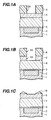
- a copper wiring 2 is embedded in the surface layer of an interlayer insulating film 1 formed on a semiconductor substrate.
- the copper wiring 2 is formed by a damascene method.
- An etching stopper film 3 of SiC having a thickness of 50 nm is formed on the interlayer insulating film 1 and copper wiring 2.
- the etching stopper film 3 can be formed by CVD using mixture gas of tetramethylsilane (Si(CH 3 ) 4 ), ammonium (NH 3 ) and nitrogen (N 2 ).
- the SiC film formed contains Si-H bonds and C-H bonds.
- a hard mask 5 of SiC having a thickness of 100 nm is formed on the interlayer insulating film 4.
- the hard mask 5 is formed by a method similar to the method of forming the etching stopper film 3.
- a resist film 6 is coated on the hard mask 5, the resist film having an opening 6A partially overlapping the wiring 2 as viewed along a line parallel to the normal to the substrate surface.
- the hard mask is dry-etched to form an opening 5A through the hard mask 5.
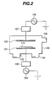
- Fig. 2 is a schematic diagram showing the structure of a reactive ion etching (RIE) system to be used for etching the hard mask 5.
- RIE reactive ion etching
- a chamber 100 a lower electrode 101 and an upper electrode 102 are disposed generally in parallel.
- Etching gas is introduced via a gas inlet port 109 into the chamber 100, whereas unreacted etching gas and reaction byproducts are drained from an air outlet port 103.
- a power source 106 applies a high frequency voltage of 27 MHz to the upper electrode 102 via an impedance matching circuit 107.
- a bias power source 104 applies a high frequency voltage of 800 kHz to the lower electrode 101 via an impedance matching circuit 105.
- a substrate 110 to be processed is placed on the lower electrode 101.
- Etching gasses used were mixture gas of CHF 3 , NF 3 , Ar and O 2 at flow rates of 20 sccm, 10 sccm, 200 sccm, and 5 sccm, respectively.
- a pressure in the chamber 100 was 6.65 Pa (50 mTorr)
- a source power supplied to the upper electrode 102 was 2000 W
- a bias power supplied to the lower electrode 101 was 1400 W
- a temperature of the lower electrode 101 was 20 °C.
- the opening 5A was able to be formed through the hard mask 5.
- the interlayer insulating film 4 is etched and then the etching stopper film 3 is etched to form a via hole. This etching is performed to lose the resist film 6.
- Fig. 1C is a cross sectional view of a substrate illustrating a comparison example in which the hard mask 5 is etched by using etching gas not containing NF 3 .
- Etching gasses used were mixture gas of CF 4 , CHF 3 , Ar and O 2 at flow rates of 20 sccm, 30 sccm, 200 sccm, and 8 sccm, respectively.
- a pressure in the chamber 100 was 5.3 Pa (40 mTorr)
- a source power supplied to the upper electrode 102 was 2500 W
- a bias power supplied to the lower electrode 101 was 1500 W
- a temperature of the lower electrode 101 was 20 °C.
- a ratio (etching selection ratio) of an etching rate of the SiC film to an etching rate of the resist film is small.
- the resist mask 6 is therefore etched before the opening is formed through the hard mask 5. The opening was not able to be formed through the hard mask 5.
- CF 4 promotes etching and CHF 3 raises an etching selection ratio of a film to be etched to a resist film. It can be known that although the etching gasses used can provide resent a sufficient etching selection ratio when a SiN film is etched, they cannot provide a sufficient etching selection ratio when a SiC film which contains hydrogen is etched.
- NF 3 gas As described above, by adding NF 3 gas to the etching gasses, a sufficient etching selection ratio can be attained and the SiC film which contains hydrogen can be etched.
- Ar added to the etching gasses is used for ion assistance, and O 2 gas has a function of improving clearance of etching.
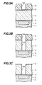
- a Cu wiring 12 is buried in a groove formed in a surface layer of an interlayer insulating film 11 formed on a semiconductor substrate.
- the copper wiring 12 can be formed by a damascene method.
- An etching stopper film 13 of SiC having a thickness of 50 nm is formed on the interlayer insulating film 11 and copper wiring 12.
- the etching stopper film 13 is formed by a method similar to the method of forming the etching stopper film 3 of the first embodiment shown in Figs. 1A and 1B.
- an interlayer insulating film 14 of SiO 2 having a thickness of 1000 nm is formed by plasma enhanced chemical vapor deposition.
- an antireflection film 15 of SiN having a thickness of 50 nm is formed by plasma enhanced chemical vapor deposition.
- a resist film 16 is coated on the antireflection film 15, the resist film having an opening 16A partially overlapping the wiring 12 as viewed along a line parallel to the normal to the substrate surface.
- the antireflection film 15 is dry-etched by using mixture gas of, for example, CHF 3 and O 2 .
- the interlayer insulating film 14 is etched by using the RIE system shown in Fig. 2.
- etching gasses used are mixture gas of C 4 F 8 , C 5 F 8 , Ar, CO and O 2 .
- the ratio (etching selection ratio) of an etching rate of the interlayer insulating film 14 to an etching rate of the etching stopper film 13 is high, the etching can be stopped almost when the etching stopper film 13 is exposed.
- a via hole 14A exposing a partial surface of the etching stopper film 13 on the bottom thereof can therefore be formed.
- the resist film 16 is ashed and removed.
- the surface of the wiring 12 is covered with the etching stopper film 13, the surface of the wiring 12 can be prevented from being oxidized.
- the etching stopper film 13 exposed on the bottom of the via hole 14A is dry-etched by using the RIE system shown in Fig. 2.
- Etching gasses used were mixture gas of CHF 3 , NF 3 , Ar and O 2 at flow rates of 30 sccm, 10 sccm, 200 sccm, and 8 sccm, respectively.
- a pressure in the chamber 100 was 6.65 Pa (50 mTorr)
- a source power supplied to the upper electrode 102 was 2000 W
- a bias power supplied to the lower electrode 101 was 1500 W
- a temperature of the lower electrode 101 was 20 °C.
- a partial surface area of the wiring 12 is therefore exposed on the bottom of the via hole 14A.
- the antireflection film 15 of SiN formed on the surface of the interlayer insulating film 14 is also etched and the upper surface of the interlayer insulating film 14 is exposed.
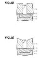
- the etching stopper film 13 exposed on the bottom of the via hole 14A can be removed almost reliably.
- Fig. 3E is a cross sectional view of a substrate illustrating a comparison example in which the etching is performed by using gasses not containing NF 3 .
- Etching gasses used were mixture gas of CHF 3 , Ar and O 2 at flow rates of 30 sccm, 200 sccm, and 8 sccm, respectively.
- a pressure in the chamber 100 was 6.65 Pa (50 mTorr)
- a source power supplied to the upper electrode 102 was 2000 W
- a bias power supplied to the lower electrode 101 was 1500 W
- a temperature of the lower electrode 101 was 20 °C.
- the etching selection ratio of the etching stopper film 13 to the interlayer insulating film 14 is not sufficient. It is therefore difficult to reliably remove the etching stopper film 13 exposed on the bottom of the via hole 14A, and the upper region of the interlayer insulating film 14 near the via hole 14A is etched.
- the etching stopper film 13 made of SiC which contains hydrogen and exposed on the bottom of the via hole 14A can be removed almost reliably and the underlying wiring can be exposed.
- a semiconductor device manufacture method according to a third embodiment of the invention will be described.
- a via hole is formed through the interlayer insulating film on the copper wiring.
- an opening for disposing a bonding pad is formed.
- a copper wiring 22 is buried in a groove formed in a surface layer of an interlayer insulating film 21 formed on a semiconductor substrate.
- an etching stopper film 23 of SiC having a thickness of 50 nm, a protective film 24 of SiO 2 having a thickness of 400 nm and a cover film 25 of SiC having a thickness of 300 nm are sequentially formed.
- the etching stopper film 23 and cover film 25 are formed by plasma enhanced chemical vapor deposition similar to forming the etching stopper film 3 of the first embodiment shown in Fig. 1A.
- the protective film 24 is formed by plasma enhanced chemical vapor deposition similar to forming the interlayer insulating film 14 of the second embodiment shown in Fig. 3A.
- a resist film 26 with an opening 26A is coated on the cover film 25.
- the opening 26A is included in the area of the wiring 22 as viewed along a line parallel to the normal to the substrate surface.
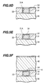
- the cover film 25 is etched to form a recess 27.
- This etching is performed under the same etching conditions as those for etching the etching stopper film 13 of the second embodiment described with Fig. 3D.
- the recess 27 reaches the middle of the protective film 24 in the depth direction.
- the protective film 24 is further etched to expose the etching stopper film 23 on the bottom of the recess 27.
- the protective film 24 is etched under the same etching conditions as those for etching the interlayer insulating film 14 of the second embodiment shown in Fig. 3B.
- the resist film 26 left on the cover film 25 is ashed and removed.
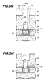
- the etching stopper film 23 exposed on the bottom of the recess 27 is etched. This etching is performed under the same etching conditions as those for etching the etching stopper film 13 of the second embodiment described with Fig. 3D.
- the copper wiring 22 is therefore exposed on the bottom of the recess 27.
- An Al film is formed covering the surface of the cover film 25 and the inner surface of the recess 27, and then patterned to form a bonding pad 28.
- the etching process for the cover film 25 shown in Fig. 4B is performed by using mixture gas of CHF 3 and NF 3 . It is therefore possible to form with good reproductivity the recess 27 through the cover film 25 made of hydrogenated SiC. Etching by using fluorocarbon gas not added with NF 3 cannot attain a sufficiently high etching selection ratio of the cover film 25 to the resist film 26. Therefore, as shown in Fig. 4F, the resist film 26 is thinned more and the recess 27 cannot be formed through the cover film 25.
- etching gasses of CHF 3 added with NF 3 are used.
- fluorocarbon gas expressed by a general formula C x H y F z (x, y and z are an integer satisfying x ⁇ 1, y ⁇ 0 and z ⁇ 1) may be used.
- SF 6 having a similar nature as NF 3 may also be used.
- an interlayer insulating film 30 is formed on a semiconductor substrate.
- a wiring layer insulating film 31 of FSG having a thickness of 500 nm is formed.
- the wiring layer insulating film 31 can be formed by plasma enhanced chemical vapor deposition by using SiH 4 , SiF 4 , N 2 O and N 2 as source gasses.
- a wiring groove 31A is formed through the wiring layer insulating film 31.
- Etching the wiring layer insulating film 31 can be performed by RIE by using mixture gas of C 4 F 8 , C 5 F 8 , Ar, CO and O 2 .
- An etching stopper film of SiN or the like may be inserted between the interlayer insulating film 30 and wiring layer insulating film 31 to control the depth of the wiring groove 31A.
- a barrier metal layer 32 of TaN having a thickness of 25 nm is formed by sputtering, the barrier metal layer covering the surface of the wiring layer insulating film 31 and the inner surface of the wiring groove 31A.
- a seed copper layer of 200 nm in thickness is formed on the surface of the barrier metal layer 32 by sputtering.
- a copper film 33L of 1300 nm in thickness is formed by plating. The copper film 33L completely buries the inner space of the wiring groove 31A.
- CMP chemical mechanical polishing
- a barrier metal layer 34 of TaN is formed by sputtering, the barrier metal layer 34 covering the surfaces of the copper wiring 33 and wiring layer insulating film 31.
- the thickness of the barrier metal layer 34 is set so that the depression of the copper wiring 33 formed by dishing is buried with the carrier metal layer 34.
- a second CMP is performed to remove an unnecessary barrier metal layer 34 excepting that inside of the wiring groove 31A.
- the copper wiring 33 is therefore formed inside the wiring groove 31A, the sidewalls, upper and bottom surfaces of the copper wiring being covered with the metal barrier layers 32 and 34.
- etch-back may be performed.
- the first CMP may remove only the copper film 33L shown in Fig. 5B to leave the barrier metal layer 32 on the wiring layer insulating film 31, and the second CMP removes the barrier metal layer 32 together with the barrier metal layer 34 shown in Fig. 5D.
- an etching stopper film 41 of SiC having a thickness of 50 nm, an interlayer insulating film 42 of FSG and an antireflection film 43 of SiN having a thickness of 50 nm are sequentially formed on the wiring layer insulating film 31 and copper wiring 33.
- the etching stopper film 41 is formed by a method similar to that of forming the etching stopper film 3 of the first embodiment shown in Fig. 1A.
- the interlayer insulating film 42 is formed by a method similar to that of forming the underlying wiring insulating film 31.
- the antireflection film 43 is formed by a method similar to that of forming the antireflection film of the second embodiment shown in Fig. 3A.
- a resist film 44 is formed on the antireflection film 43.
- An opening 44A corresponding to a via hole is formed through the resist film 44.
- the opening 44A is positioned in a partial surface area of the copper wiring 33 as viewed along a line parallel to the normal to the substrate surface.
- the resist mask 44 as an etching mask, the antireflection film 43 and interlayer insulating film 42 are etched to the middle of the interlayer insulating film 42 in the depth direction to thereby form a via hole 45.
- the resist film 44 is thereafter removed.
- a resist film 47 is formed on the surface of the antireflection film 43.
- An opening 47A corresponding to a wiring groove is formed through the resist film 47.
- the opening 47A is positioned superposed upon the via hole 45.
- the antireflection film 43 and interlayer insulating film 42 are etched. Therefore, a wiring groove 46 corresponding to the opening 47A is formed and the via hole 45 is further etched to expose a partial surface area of the etching stopper film 41 on the bottom of the via hole 45.
- the etching stopper film 41 exposed on the bottom of the via hole 45 is dry-etched to expose the underlying barrier metal layer 34.
- the etching conditions for the etching stopper film 41 will be described.
- Etching gasses used were mixture gas of CHF 3 , SF 6 , Ar and O 2 at flow rates of 30 sccm, 10 sccm, 200 sccm and 8 sccm, respectively.
- a pressure in the chamber 100 was 6.65 Pa (50 mTorr)
- a source power supplied to the upper electrode 102 was 2000 W
- a bias power supplied to the lower electrode 101 was 1500 W
- a temperature of the lower electrode 101 was 20 °C.
- the etching stopper film 41 on the bottom of the via hole 45 can be almost reliably etched. If copper is exposed on the etched surface, it is more preferable to add NF 3 to fluorocarbon gas than SF 6 in order to prevent corrosion of copper.
- the upper surface of the copper wiring 33 is covered with the barrier metal layer 34 of TaN, SF 6 can be used.
- the barrier metal layer Ta, Ti or TiN may be used in place of TaN.
- an SiC film which contains hydrogen is etched by using mixture gas of fluorocarbon added with SF 6 or NF 3 .
- Both SF 6 and NF 3 gasses may be added to fluorocarbon gas.
- CHF 3 is used as fluorocarbon gas
- gas expressed by a general formula C x H y F z (x, y and z are an integer satisfying x ⁇ 1, y ⁇ 0 and z ⁇ 1) may be used.
- Examples of such gas are CF 4 , CH 2 F 2 , C 4 F 8 , C 5 F 8 , C 4 F 6 and the like.
- High effects of adding NF 3 or SF 6 to etching gas can be obtained when a SiC film which contains hydrogen, particularly hydrogen of 20 atom %, is etched. It is preferable to set the hydrogen content to 50 atom % or less when an SiC film is used as a hard mask or an etching stopper film.
- an interlayer insulating film As the material of an interlayer insulating film, SiLK (the Dow Chemical Company), SiO 2 , or FSG is used. Other insulating materials may also be used which have different etching resistance from that of SiC.
- an interlayer insulating film may be a film made of phosphosilicate glass (PSG), a film of borophosphosilicate glass (BPSG), a film of hydrogen silsesquioxane (HSQ), a deposited film of tetraethylorthosilicate (TEOS), a film made by spin-on-glass, a film of carbon-containing silicon oxide (SiOC), a silicon-containing foaming porous film, an insulating film of organic material, or the like.
- Examples of the material of an organic insulating film are poly(aryl ether)s, i.e., FLARE of Allied Signal Inc.
- etching systems may also be used such as an electron cyclotron resonance plasma (ECR plasma) etching system, an inductive coupled plasma (ICP) etching system and a helicon plasma etching system.
- ECR plasma electron cyclotron resonance plasma
- ICP inductive coupled plasma
- mixture gas of Si(CH 3 )) 4 , NH 3 and N 2 is used as the source gasses for forming an SiC film by plasma enhanced chemical vapor deposition.
- Other gasses may also be used.
- mixture gas of Si(CH 3 ) 3 H, NH 3 and He may be used.
- the SiC film made of these source gasses is known by the merchandise name BLOk of Applied Materials Inc.
- the semiconductor device manufacture methods are characterized in a process of etching an SiC film which contains hydrogen.
- the fifth embodiment is characterized in a method of forming an SiC film.
- the etching stopper film 13 of SiC of the second embodiment shown in Fig. 3B has a function of an etching stopper film when the via hole 14A is formed through the upper level interlayer insulating film 14. It is therefore necessary that under the etching conditions for the interlayer insulating film 14, the etching rate of the etching stopper film 13 is sufficiently slower than that of the interlayer insulating film 14.
- An etching selection ratio of an SiO 2 film to an SiN film used as a conventional etching stopper film is about 9.5. It is known that an etching selection ratio of an SiO 2 film to an SiC film lowers to about 7. An etching selection ratio, particularly an etching selection ratio when an etching stopper film on the bottom of a via hole is used, lowers considerably. An etching selection ratio of an FSG film to an SiN film on the bottom of a via hole was about 28, whereas an etching selection ratio of an FSG film on an SiC film on the bottom of a via hole was about 17. A large reduction amount of the etching selection ratio when the etching is to be stopped at the bottom of the via hole may be ascribed to that the etching on the bottom of the via hole is governed more by chemical reaction than by sputtering.
- Fig. 6 is a graph showing the results of Fourier transform infrared (FT-IR) spectroscopy of an SiC film having a relatively low etching rate under the etching conditions of SiO 2 or FSG.
- the abscissa represents a wave number in the unit of cm -1 and the ordinate represents an absorbance. It can be seen that not only a peak caused by Si-C bonds but also a peak caused by Si-OCH bonds appear. The peak caused by Si-OCH bonds is more intense than the peak caused by Si-C bonds. It can be considered that since the Si-C film contains more Si-OCH bonds, the etching rate of the SiC film under the SiO etching conditions became fast.
- FT-IR Fourier transform infrared
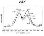
- Fig. 7 is a graph showing the results of FT-IR spectroscopy of five SiC films formed under different film forming conditions.
- the Si-C films were formed by using tetramethylsilane and CO 2 as source gasses. Numerical values affixed to curves shown in Fig. 7 represent ratios of flow rates of tetramethylsilane to flow rates of CO 2 .
- Fig. 8 is a graph showing a relation between a flow rate ratio between tetramethylsilane and CO 2 when SiC films are formed and an etching rate of each SiC film.
- the abscissa represents a ratio of a flow rate of tetramethylsilane to a flow rate of CO 2
- the ordinate represents an etching rate in the unit of "nm/min”.
- the etching conditions used were as follows.
- a flow rate of C 4 F 8 was 8 sccm, that of C 5 F 8 was 3 sccm, that of Ar was 320 sccm, that of CO was 190 sccm, and that of O 2 was 8 sccm.
- a pressure was about 4 Pa (30 mTorr), a source power was 1750 W, a bias power was 1400 W and a lower electrode temperature was 20 °C.
- the flow rate ratio is 0.2 or higher, the etching rates are scarcely influenced by the flow rates and distribute around 30 nm/min. It can be seen that the etching rate becomes fast in the range lower than 0.2. It is therefore preferable that the flow rate ratio between the source gasses is set to 0.2 or higher if the SiC film is utilized as an etching stopper film.
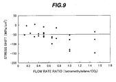
- Fig. 9 is a graph showing a relation between a flow rate ratio between tetramethylsilane and CO 2 when SiC films are formed and a stress shift.
- the abscissa represents a ratio of a flow rate of tetramethylsilane to a flow rate of CO 2
- the ordinate represents a stress shift in the unit of "MPa/cm 2 ".
- the stress shift was measured as a warp of each substrate after 10 to 12 days after the films were formed. It can be known that as the flow rate ratio is made large, the stress shift becomes large in the negative direction. Samples having large absolute values of stress shifts are found in a range particularly over a flow rate ratio of 0.6. A large stress shift means instability of the quality of an SiC film. It is therefore preferable to set the flow rate ratio to 0.6 or smaller.
- an etching rate under the etching conditions for an SiO 2 film is slow and if the stable quality of an SiC film is to be obtained, it is preferable to set the ratio of a flow rate of tetramethylsilane to a flow rate of CO 2 to a range from 0.2 to 0.6, or more preferably to a range from 0.3 to 0.5.
- a silicon substrate 51 has on its surface an element separation insulating region 52.
- the element separation insulating region 52 is formed by silicon local oxidation (LOCOS) or shallow trench isolation (STI).
- An active region surrounded by the element separation insulating region 52 has a MOSFET including a gate electrode 53G, a source region 53S and a drain region 53D.
- the upper surface of the gate electrode 53G has an upper insulating film 531 of SiO 2 .
- the sidewalls of the gate electrode 53G and upper insulating film 531 have sidewall spacers 53W.
- MOSFET 53 can be formed by repeating well-known photolithography, etching, ion implantation and the like.
- an etching stopper film 57 made of SiC is formed covering MOSFET 53.
- the etching stopper film 57 is formed under the preferable film forming conditions described with the fifth embodiment.
- an interlayer insulating film 60 of phosphosilicate glass (PSG) having a thickness of 500 nm is formed by chemical vapor deposition (CVD) and CMP.
- a resist mask 61 is formed on the surface of the interlayer insulating film 60. Openings are formed through the resist film 61 in the areas corresponding to the source region 53S and drain region 53D.
- the interlayer insulating film 60 is etched to form contact holes 62S and 62D in the areas corresponding to the source region 53S and drain region 53D. This etching stops at the etching stopper film 57. The resist film 61 is thereafter removed.
- the contact hole 62D partially overlaps the gate electrode 53G as viewed along a line parallel to the normal to the substrate surface.
- the etching stopper film 57 exposed on the bottom of the contact holes 62S and 62D is removed. This etching is performed under the preferable etching conditions described with the second embodiment. Partial surface areas of the source region 53S and drain region 53D are therefore exposed. Since the upper insulating film 531 is disposed on the gate electrode 53G, the gate electrode 53G is not exposed.
- a barrier metal layer of 30 nm in thickness is formed covering the inner surfaces of the contact holes 62S and 62D and the upper surface of the etching stopper film 57.
- the barrier metal layer 63 is made of Ti, TiN or TaN.
- a tungsten (W) layer is formed which has a thickness sufficient for burying the insides of the contact holes 62S and 62D with the tungsten layer.
- the barrier metal layer and W layer are formed by CVD.
- CMP is performed until the interlayer insulating film 60 is exposed to remove an unnecessary barrier metal layer and W layer. Conductive plugs 64 made of the barrier metal layer 63 and W layer are therefore left in the contact holes 62S and 62D.
- an etching stopper film 69 of SiC having a thickness of 50 nm is formed on the interlayer insulating film 60.
- a first wiring layer insulating film 70 of 250 nm in thickness is formed.
- the first wiring layer insulating film 70 is made of FSG.
- a cap film 71 of SiO 2 having a thickness of 150 nm is formed by plasma enhanced chemical vapor deposition.
- a resist pattern 74 is formed on the cap film 71.
- the resist pattern 74 has openings 76 formed therethrough and corresponding to wirings to be formed in the first wiring layer insulating film 70.
- the openings 76 are formed by usual photolithography.
- the cap layer 71 and first wiring layer insulating film 70 are etched.
- the cap layer 71 and first layer wiring film 70 are etched by RIE using mixture gas of C 4 F 8 , C 5 F 8 , Ar, CO and O 2 as etching gasses. This etching stops at the etching stopper film 69.
- Wiring grooves 75 corresponding to the openings 76 of the resist pattern 74 are therefore formed through the first wiring layer insulating film 70.
- the resist pattern 74 is removed. Thereafter, the etching stopper film 69 exposed on the bottoms of the wiring grooves 75 is removed.
- the upper surface of the conductive plug 64 is exposed on the bottom of the corresponding wiring groove 75.
- a barrier metal layer 72L of 25 nm in thickness is formed covering the inner surfaces of the wiring grooves 75 and the upper surface of the cap film 71.
- the barrier metal layer 72L is made of TiN or TaN and formed by sputtering.
- a conductive layer 73L of copper is formed on the surface of the barrier layer 72L.
- the conductive layer 73L is formed by covering the surface of the barrier metal layer 72L with a seed layer of Cu and then plating Cu, and has a thickness sufficient for burying the insides of the wiring grooves 75 with the conductive layer.
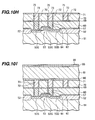
- a diffusion barrier film 80 of SiC having a thickness of 50 nm, an interlayer insulating film 81 of FSG having a thickness of 800 nm, a cap film 85 of SiO 2 having a thickness of 100 nm and a hard mask 86 of SiC having a thickness of 50 nm are sequentially deposited.
- the diffusion barrier film 80 is formed by the preferred film forming conditions described with the fifth embodiment, and the hard mask 86 is formed under the same conditions as those of forming the hard mask 5 of the first embodiment shown in Fig. 1A.
- the hard mask 86 is patterned to form openings 87.
- the openings 87 correspond to wiring patterns to be formed in the wiring layer insulating film 81.
- the hard mask 86 is patterned under the conditions similar to those of etching the hard mask 5 of the first embodiment shown in Fig. 1B.
- a resist pattern 90 is formed on the cap film 85 exposed on the bottoms of the openings 87 and on the hard mask 86.
- the resist pattern 90 has openings 91 corresponding to via holes to be formed through the interlayer insulating film 81. As viewed along a line parallel to the normal to the substrate surface, the openings 91 are included in the openings 87 formed through the hard mask 86.
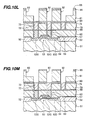
- the cap film 85 is etched and the interlayer insulating film 81 is etched to the intermediate depth thereof to form via holes 92.
- the resist pattern 90 is ashed and removed
- the interlayer insulating film 81 is etched from its upper surface to the intermediate depth to form wiring grooves 93.
- the bottom of the via hole 92 is further etched and the via hole 92 is eventually formed through the intermediate insulating film 81.
- This etching can be performed by RIE using mixture gas of C 4 F 8 , C 5 F 8 , Ar, CO and O 2 as etching gasses.
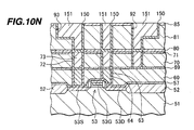
- the hard mask 86 and diffusion barrier film 80 exposed on the bottoms of the via holes 92 are etched. This etching is performed under the conditions similar to those of etching the etching stopper film 13 of the second embodiment described with Fig. 3D.
- the inner surfaces of the via holes 92 and the wiring grooves 93 are covered with a barrier metal layer 150 and the insides of the via holes and wiring grooves 93 are buried with a Cu wiring.
- the barrier metal layer 150 and Cu wiring 151 are formed by a method similar to that of forming the barrier metal layer 72 and Cu wiring 73 in the first wiring layer insulating film.
- an SiC film can be used as a hard mask or an etching stopper film.
- parasitic capacitance between wiring patterns can be reduced so that a high speed operation of a semiconductor integrated circuit device is possible.
Landscapes
- Internal Circuitry In Semiconductor Integrated Circuit Devices (AREA)
- Drying Of Semiconductors (AREA)
- Electrodes Of Semiconductors (AREA)
Abstract
Description
Claims (12)
- A method of manufacturing a semiconductor device, comprising steps of:forming a first film on a semiconductor substrate, the first film being made of material having a different etching resistance from silicon carbide;forming a second film on the first film, the second film being made of hydrogenated silicon carbide;forming a resist film with an opening on the second film;dry-etching the second film by using the resist mask as an etching mask and mixture gas of fluorocarbon gas added with at least one of SF6 and NF3; andetching the first film by using the second film as a mask.
- A method of manufacturing a semiconductor device, comprising steps of:preparing a substrate having a conductive region exposed on a partial area of an insulating surface of the substrate;forming a first film on the surface of the substrate, the first film being made of hydrogenated silicon carbide;forming a second film made of insulating material on the first film;forming a resist film with an opening on the second film;etching the second film by using the resist mask as an etching mask to form a recess and expose a partial surface area of the first film on the bottom of the recess;ashing and removing the resist film;dry-etching the first film exposed on the bottom of the recess by using mixture gas of fluorocarbon gas added with at least one of SF6 and NF3 to expose the conductive region of the substrate; and
- A method according to claim 2, wherein the conductive region exposed on the partial area of the insulating surface of the substrate is a copper wiring.
- A method according to claim 3, wherein an upper surface of the copper wiring is covered with a barrier metal layer made of material selected from a group consisting of Ta, TaN, Ti and TiN.
- A method according to claim 2, wherein the second film is a film selected from a group consisting of a silicon oxide film, a film of phosphosilicate glass, a film of borophosphosilicate glass, a film of fluorosilicate glass, a film of hydrogen silsesquioxane, a film deposited using tetraethylorthosilicate as a source, a film formed by spin-on-glass, a film of carbon-containing silicon oxide, a silicon-containing foaming porous film, and an insulating film of organic material.
- A method according to claim 2, wherein the step of forming the first film forms the first film by chemical vapor deposition using tetramethylsilane and carbon dioxide as source gasses and by setting a ratio of a flow rate of tetramethylsilane to a flow rate of carbon dioxide to a range from 0.2 to 0.6.
- A method of manufacturing a semiconductor device, comprising steps of:preparing a substrate having a conductive member exposed on a partial area of an insulating surface of the substrate;forming a first film on the surface of the substrate, the first film being made of hydrogenated silicon carbide;forming a second film made of insulating material on the first film, the insulating material having a different etching resistance from silicon carbide;forming a third film on the second film, the third film being made of hydrogenated silicon carbide;forming a resist film with an opening on the third film, the opening overlapping with a partial area of the conductive member as viewed along a line parallel to a normal to the substrate surface;etching the third film by using the resist mask as an etching mask and using mixture gas of fluorocarbon gas added with at least one of SF6 and NF3;etching the second film by using the resist mask as an etching mask under a condition that an etching rate of the second film is faster than an etching rate of the first film, to form a recess and expose a partial surface area of the first film on a bottom of the recess;ashing and removing the resist film; anddry-etching the first film exposed on the bottom of the recess by using mixture gas of fluorocarbon gas added with at least one of SF6 and NF3, to expose the conductive member of the substrate.
- A method according to claim 7, wherein the step of forming the first film the first film is formed by chemical vapor deposition using tetramethylsilane and carbon dioxide as source gasses and by setting a ratio of a flow rate of tetramethylsilane to a flow rate of carbon dioxide to a range from 0.2 to 0.6.
- A method of manufacturing a semiconductor device, comprising steps of:preparing a substrate having a wiring exposed on a partial area of an insulating surface of the substrate;forming a first film on the surface of the substrate, the first film being made of hydrogenated silicon carbide;forming a second film made of insulating material on the first film, the insulating material having a different etching resistance from silicon carbide;forming a third film on the second film, the third film being made of hydrogenated silicon carbide;forming a first resist film with a first opening on the third film, the first opening overlapping with a partial area of the conductive member as viewed along a line parallel to a normal to the substrate surface;etching the third film by using the resist mask as an etching mask and using mixture gas of fluorocarbon gas added with at least one of SF6 and NF3 to expose a partial surface of the second film;removing the first resist film;forming a second resist film with a second opening on surfaces of the etched third film and exposed second film, the second opening being included in an area of the first opening and partially overlapping with the wiring;etching the second film at least to an intermediate depth thereof by using the second resist mask as an etching mask;removing the second resist film;etching the third film by using the partially etched third film as a mask to form a via hole reaching the first film in an area where the second opening is formed, and to form a wiring groove to an intermediate depth of the second film in an area where the first opening is formed and the second opening is not formed;dry-etching the first film exposed on the bottom of the via hole by using mixture gas of fluorocarbon gas added with at least one of SF6 and NF3, to expose the wiring; andburying insides of the via hole and wiring groove with a conductive member.
- A method according to claim 9, wherein the step of forming the first film the first film is formed by chemical vapor deposition using tetramethylsilane and carbon dioxide as source gasses and by setting a ratio of a flow rate of tetramethylsilane to a flow rate of carbon dioxide to a range from 0.2 to 0.6.
- A method of manufacturing a semiconductor device, comprising steps of:forming a first film of silicon carbide on a surface of a semiconductor substrate by chemical vapor deposition using tetramethylsilane and carbon dioxide as source gasses and by setting a ratio of a flow rate of tetramethylsilane to a flow rate of carbon dioxide to a range from 0.2 to 0.6;forming a second film on the first film, the second film being made of insulating material having a different etching resistance from silicon carbide;forming a resist film with an opening; andetching the second film by using the resist film as an etching mask under a condition that an etching rate of the second film is faster than an etching rate of the first film to partially expose the first film.
- A method according to claim 11, wherein the second film is made of fluorosilicate glass.
Applications Claiming Priority (2)
| Application Number | Priority Date | Filing Date | Title |
|---|---|---|---|
| JP2001312883A JP2003124189A (en) | 2001-10-10 | 2001-10-10 | Method for manufacturing semiconductor device |
| JP2001312883 | 2001-10-10 |
Publications (2)
| Publication Number | Publication Date |
|---|---|
| EP1302981A2 true EP1302981A2 (en) | 2003-04-16 |
| EP1302981A3 EP1302981A3 (en) | 2004-06-02 |
Family
ID=19131463
Family Applications (1)
| Application Number | Title | Priority Date | Filing Date |
|---|---|---|---|
| EP02002111A Withdrawn EP1302981A3 (en) | 2001-10-10 | 2002-01-28 | Method of manufacturing semiconductor device having silicon carbide film |
Country Status (6)
| Country | Link |
|---|---|
| US (1) | US20030068582A1 (en) |
| EP (1) | EP1302981A3 (en) |
| JP (1) | JP2003124189A (en) |
| KR (1) | KR20030030838A (en) |
| CN (1) | CN1222030C (en) |
| TW (1) | TW522519B (en) |
Cited By (3)
| Publication number | Priority date | Publication date | Assignee | Title |
|---|---|---|---|---|
| WO2006025944A1 (en) * | 2004-08-26 | 2006-03-09 | Tokyo Electron Limited | Method and system for etching a gate stack |
| DE102004062835B4 (en) * | 2003-12-31 | 2006-12-21 | Dongbuanam Semiconductor Inc. | Method of forming a dual damascene structure |
| US10644039B2 (en) | 2014-10-01 | 2020-05-05 | Semiconductor Energy Laboratory Co., Ltd. | Wiring layer and manufacturing method therefor |
Families Citing this family (31)
| Publication number | Priority date | Publication date | Assignee | Title |
|---|---|---|---|---|
| US7687917B2 (en) * | 2002-05-08 | 2010-03-30 | Nec Electronics Corporation | Single damascene structure semiconductor device having silicon-diffused metal wiring layer |
| JP4071069B2 (en) * | 2002-08-28 | 2008-04-02 | 東京エレクトロン株式会社 | Insulating film etching method |
| JP2004296835A (en) * | 2003-03-27 | 2004-10-21 | Applied Materials Inc | Method of forming damascene structure |
| US6903011B2 (en) * | 2003-06-05 | 2005-06-07 | Taiwan Semiconductor Manufacturing Company, Ltd. | Displacement method to grow cu overburden |
| JP4057972B2 (en) | 2003-07-25 | 2008-03-05 | 富士通株式会社 | Manufacturing method of semiconductor device |
| JP3866694B2 (en) * | 2003-07-30 | 2007-01-10 | 株式会社日立ハイテクノロジーズ | LSI device etching method and apparatus |
| TWI250558B (en) * | 2003-10-23 | 2006-03-01 | Hynix Semiconductor Inc | Method for fabricating semiconductor device with fine patterns |
| US7517801B1 (en) * | 2003-12-23 | 2009-04-14 | Lam Research Corporation | Method for selectivity control in a plasma processing system |
| CN100433256C (en) * | 2004-03-18 | 2008-11-12 | 克里公司 | Sequential photolithography method to reduce stacking fault nucleation sites and structure with reduced stacking fault nucleation sites |
| US7173285B2 (en) * | 2004-03-18 | 2007-02-06 | Cree, Inc. | Lithographic methods to reduce stacking fault nucleation sites |
| US8222155B2 (en) | 2004-06-29 | 2012-07-17 | Lam Research Corporation | Selectivity control in a plasma processing system |
| JP4615290B2 (en) * | 2004-11-16 | 2011-01-19 | 東京エレクトロン株式会社 | Plasma etching method |
| US7915735B2 (en) * | 2005-08-05 | 2011-03-29 | Micron Technology, Inc. | Selective metal deposition over dielectric layers |
| US20070048991A1 (en) * | 2005-08-23 | 2007-03-01 | Taiwan Semiconductor Manufacturing Co., Ltd. | Copper interconnect structures and fabrication method thereof |
| US20070218699A1 (en) * | 2006-03-16 | 2007-09-20 | Tokyo Electron Limited | Plasma etching method and computer-readable storage medium |
| US7375021B2 (en) * | 2006-04-04 | 2008-05-20 | International Business Machines Corporation | Method and structure for eliminating aluminum terminal pad material in semiconductor devices |
| JP2008053507A (en) * | 2006-08-25 | 2008-03-06 | Matsushita Electric Ind Co Ltd | Dry etching method |
| JP4948278B2 (en) * | 2006-08-30 | 2012-06-06 | ルネサスエレクトロニクス株式会社 | Manufacturing method of semiconductor device |
| CN100533678C (en) * | 2006-11-09 | 2009-08-26 | 厦门大学 | Method for reducing surface damage of SiC etched by ICP |
| US7767578B2 (en) | 2007-01-11 | 2010-08-03 | United Microelectronics Corp. | Damascene interconnection structure and dual damascene process thereof |
| CN101231968B (en) * | 2007-01-26 | 2010-11-17 | 联华电子股份有限公司 | Damascene interconnect structure and dual damascene process |
| KR100924545B1 (en) * | 2007-03-15 | 2009-11-02 | 주식회사 하이닉스반도체 | Manufacturing method of semiconductor device |
| KR100862315B1 (en) | 2007-03-23 | 2008-10-13 | 주식회사 하이닉스반도체 | Mask rework method |
| CN101157569B (en) * | 2007-09-03 | 2010-06-02 | 中国电子科技集团公司第十三研究所 | A method for non-destructive etching of silicon carbide |
| JP6249815B2 (en) * | 2014-02-17 | 2017-12-20 | 株式会社Ihi | Manufacturing method and manufacturing apparatus for heat-resistant composite material |
| JP6310816B2 (en) * | 2014-08-26 | 2018-04-11 | ルネサスエレクトロニクス株式会社 | Manufacturing method of semiconductor device |
| US10453684B1 (en) * | 2018-05-09 | 2019-10-22 | Applied Materials, Inc. | Method for patterning a material layer with desired dimensions |
| JP7629594B2 (en) * | 2021-06-22 | 2025-02-14 | 東京エレクトロン株式会社 | Film forming method and film forming apparatus |
| JP7669310B2 (en) | 2022-03-16 | 2025-04-28 | 株式会社東芝 | Semiconductor device manufacturing method, semiconductor device, inverter circuit, drive device, vehicle, and elevator |
| KR20240162659A (en) * | 2023-05-09 | 2024-11-18 | 삼성전자주식회사 | Method for fabricating semiconductor device |
| WO2026078504A1 (en) * | 2024-10-10 | 2026-04-16 | 株式会社半導体エネルギー研究所 | Semiconductor device |
Family Cites Families (14)
| Publication number | Priority date | Publication date | Assignee | Title |
|---|---|---|---|---|
| DE2364989C3 (en) * | 1973-12-28 | 1979-10-18 | Consortium Fuer Elektrochemische Industrie Gmbh, 8000 Muenchen | Process for the production of layers of silicon carbide on a silicon substrate |
| JPS58141377A (en) * | 1982-02-16 | 1983-08-22 | Seiko Epson Corp | Plasma coating method |
| JP3229002B2 (en) * | 1992-04-24 | 2001-11-12 | キヤノン株式会社 | Light receiving member for electrophotography |
| US5433823A (en) * | 1993-09-30 | 1995-07-18 | Cain; John L. | Selective dry-etching of bi-layer passivation films |
| US6413583B1 (en) * | 1998-02-11 | 2002-07-02 | Applied Materials, Inc. | Formation of a liquid-like silica layer by reaction of an organosilicon compound and a hydroxyl forming compound |
| US6287959B1 (en) * | 1998-04-23 | 2001-09-11 | Advanced Micro Devices, Inc. | Deep submicron metallization using deep UV photoresist |
| KR20020028047A (en) * | 1999-05-03 | 2002-04-15 | 맥켈러 로버트 루이스 | METHOD FOR REMOVAL OF Sic |
| US6261157B1 (en) * | 1999-05-25 | 2001-07-17 | Applied Materials, Inc. | Selective damascene chemical mechanical polishing |
| FR2802336B1 (en) * | 1999-12-13 | 2002-03-01 | St Microelectronics Sa | DAMASCENE-TYPE INTERCONNECTION STRUCTURE AND ITS MANUFACTURING METHOD |
| US6475889B1 (en) * | 2000-04-11 | 2002-11-05 | Cree, Inc. | Method of forming vias in silicon carbide and resulting devices and circuits |
| US6730597B1 (en) * | 2000-08-03 | 2004-05-04 | Texas Instruments Incorporated | Pre-ECD wet surface modification to improve wettability and reduced void defect |
| US6362094B1 (en) * | 2000-08-16 | 2002-03-26 | Agere Systems Guardian Corp. | Hydrogenated silicon carbide as a liner for self-aligning contact vias |
| US6670278B2 (en) * | 2001-03-30 | 2003-12-30 | Lam Research Corporation | Method of plasma etching of silicon carbide |
| US6717194B2 (en) * | 2001-10-30 | 2004-04-06 | Micron Technology, Inc. | Magneto-resistive bit structure and method of manufacture therefor |
-
2001
- 2001-10-10 JP JP2001312883A patent/JP2003124189A/en active Pending
-
2002
- 2002-01-28 EP EP02002111A patent/EP1302981A3/en not_active Withdrawn
- 2002-01-29 TW TW091101468A patent/TW522519B/en not_active IP Right Cessation
- 2002-01-30 US US10/058,426 patent/US20030068582A1/en not_active Abandoned
- 2002-04-10 CN CNB021062994A patent/CN1222030C/en not_active Expired - Fee Related
- 2002-06-29 KR KR1020020037574A patent/KR20030030838A/en not_active Withdrawn
Cited By (8)
| Publication number | Priority date | Publication date | Assignee | Title |
|---|---|---|---|---|
| DE102004062835B4 (en) * | 2003-12-31 | 2006-12-21 | Dongbuanam Semiconductor Inc. | Method of forming a dual damascene structure |
| US7179734B2 (en) | 2003-12-31 | 2007-02-20 | Dongbu Electronics Co., Ltd. | Method for forming dual damascene pattern |
| WO2006025944A1 (en) * | 2004-08-26 | 2006-03-09 | Tokyo Electron Limited | Method and system for etching a gate stack |
| US10644039B2 (en) | 2014-10-01 | 2020-05-05 | Semiconductor Energy Laboratory Co., Ltd. | Wiring layer and manufacturing method therefor |
| US11211408B2 (en) | 2014-10-01 | 2021-12-28 | Semiconductor Energy Laboratory Co., Ltd. | Wiring layer and manufacturing method therefor |
| US11616085B2 (en) | 2014-10-01 | 2023-03-28 | Semiconductor Energy Laboratory Co., Ltd. | Wiring layer and manufacturing method therefor |
| US11901372B2 (en) | 2014-10-01 | 2024-02-13 | Semiconductor Energy Laboratory Co., Ltd. | Wiring layer and manufacturing method therefor |
| US12183747B2 (en) | 2014-10-01 | 2024-12-31 | Semiconductor Energy Laboratory Co., Ltd. | Wiring layer and manufacturing method therefor |
Also Published As
| Publication number | Publication date |
|---|---|
| CN1222030C (en) | 2005-10-05 |
| TW522519B (en) | 2003-03-01 |
| EP1302981A3 (en) | 2004-06-02 |
| JP2003124189A (en) | 2003-04-25 |
| KR20030030838A (en) | 2003-04-18 |
| CN1411050A (en) | 2003-04-16 |
| US20030068582A1 (en) | 2003-04-10 |
Similar Documents
| Publication | Publication Date | Title |
|---|---|---|
| EP1302981A2 (en) | Method of manufacturing semiconductor device having silicon carbide film | |
| US6905968B2 (en) | Process for selectively etching dielectric layers | |
| US6815823B2 (en) | Copper metal structure for the reduction of intra-metal capacitance | |
| US6380096B2 (en) | In-situ integrated oxide etch process particularly useful for copper dual damascene | |
| US6265321B1 (en) | Air bridge process for forming air gaps | |
| US6291334B1 (en) | Etch stop layer for dual damascene process | |
| US6337282B2 (en) | Method for forming a dielectric layer | |
| US6599830B2 (en) | Semiconductor device and manufacturing method thereof | |
| US6849539B2 (en) | Semiconductor device and method of fabricating the same | |
| US6566283B1 (en) | Silane treatment of low dielectric constant materials in semiconductor device manufacturing | |
| US7564136B2 (en) | Integration scheme for Cu/low-k interconnects | |
| JP4005431B2 (en) | Wiring formation method using dual damascene process | |
| US6191028B1 (en) | Method of patterning dielectric | |
| US20080207000A1 (en) | Method of making high-aspect ratio contact hole | |
| US6232237B1 (en) | Method for fabricating semiconductor device | |
| US6265315B1 (en) | Method for improving chemical/mechanical polish uniformity over rough topography for semiconductor integrated circuits | |
| US5880030A (en) | Unlanded via structure and method for making same | |
| US20020033486A1 (en) | Method for forming an interconnection line using a hydrosilsesquioxane (HSQ) layer as an interlayer insulating layer | |
| US6787474B2 (en) | Manufacture method for semiconductor device having silicon-containing insulating film | |
| US6881661B2 (en) | Manufacturing method of semiconductor device | |
| TWI235455B (en) | Method for manufacturing semiconductor device | |
| US7488687B2 (en) | Methods of forming electrical interconnect structures using polymer residues to increase etching selectivity through dielectric layers | |
| KR100483838B1 (en) | Dual damascene process of metal wire | |
| US20020009893A1 (en) | Method of forming a conductor in a fluoride silicate glass (FSG) layer | |
| KR20010025972A (en) | Method of forming interconnection layer in semiconductor device |
Legal Events
| Date | Code | Title | Description |
|---|---|---|---|
| PUAI | Public reference made under article 153(3) epc to a published international application that has entered the european phase |
Free format text: ORIGINAL CODE: 0009012 |
|
| AK | Designated contracting states |
Designated state(s): AT BE CH CY DE DK ES FI FR GB GR IE IT LI LU MC NL PT SE TR |
|
| AX | Request for extension of the european patent |
Extension state: AL LT LV MK RO SI |
|
| 17P | Request for examination filed |
Effective date: 20040204 |
|
| PUAL | Search report despatched |
Free format text: ORIGINAL CODE: 0009013 |
|
| AK | Designated contracting states |
Kind code of ref document: A3 Designated state(s): AT BE CH CY DE DK ES FI FR GB GR IE IT LI LU MC NL PT SE TR |
|
| AX | Request for extension of the european patent |
Extension state: AL LT LV MK RO SI |
|
| AKX | Designation fees paid | ||
| RBV | Designated contracting states (corrected) |
Designated state(s): DE FR IT |
|
| REG | Reference to a national code |
Ref country code: DE Ref legal event code: 8566 |
|
| RBV | Designated contracting states (corrected) |
Designated state(s): DE FR IT |
|
| STAA | Information on the status of an ep patent application or granted ep patent |
Free format text: STATUS: THE APPLICATION IS DEEMED TO BE WITHDRAWN |
|
| 18D | Application deemed to be withdrawn |
Effective date: 20060801 |