EP1302976A1 - Single crystal wafer and solar battery cell - Google Patents
Single crystal wafer and solar battery cell Download PDFInfo
- Publication number
- EP1302976A1 EP1302976A1 EP01947892A EP01947892A EP1302976A1 EP 1302976 A1 EP1302976 A1 EP 1302976A1 EP 01947892 A EP01947892 A EP 01947892A EP 01947892 A EP01947892 A EP 01947892A EP 1302976 A1 EP1302976 A1 EP 1302976A1
- Authority
- EP
- European Patent Office
- Prior art keywords
- single crystal
- plane
- wafer
- silicon
- oxide film
- Prior art date
- Legal status (The legal status is an assumption and is not a legal conclusion. Google has not performed a legal analysis and makes no representation as to the accuracy of the status listed.)
- Granted
Links
Images

Classifications
-
- H—ELECTRICITY
- H10—SEMICONDUCTOR DEVICES; ELECTRIC SOLID-STATE DEVICES NOT OTHERWISE PROVIDED FOR
- H10P—GENERIC PROCESSES OR APPARATUS FOR THE MANUFACTURE OR TREATMENT OF DEVICES COVERED BY CLASS H10
- H10P95/00—Generic processes or apparatus for manufacture or treatments not covered by the other groups of this subclass
-
- H—ELECTRICITY
- H10—SEMICONDUCTOR DEVICES; ELECTRIC SOLID-STATE DEVICES NOT OTHERWISE PROVIDED FOR
- H10D—INORGANIC ELECTRIC SEMICONDUCTOR DEVICES
- H10D64/00—Electrodes of devices having potential barriers
- H10D64/01—Manufacture or treatment
- H10D64/013—Manufacture or treatment of electrodes having a conductor capacitively coupled to a semiconductor by an insulator
- H10D64/01302—Manufacture or treatment of electrodes having a conductor capacitively coupled to a semiconductor by an insulator the insulator being formed after the semiconductor body, the semiconductor being silicon
- H10D64/01332—Making the insulator
- H10D64/01336—Making the insulator on single crystalline silicon, e.g. chemical oxidation using a liquid
- H10D64/01346—Making the insulator on single crystalline silicon, e.g. chemical oxidation using a liquid in a gaseous ambient using an oxygen or a water vapour, e.g. oxidation through a layer
-
- C—CHEMISTRY; METALLURGY
- C30—CRYSTAL GROWTH
- C30B—SINGLE-CRYSTAL GROWTH; UNIDIRECTIONAL SOLIDIFICATION OF EUTECTIC MATERIAL OR UNIDIRECTIONAL DEMIXING OF EUTECTOID MATERIAL; REFINING BY ZONE-MELTING OF MATERIAL; PRODUCTION OF A HOMOGENEOUS POLYCRYSTALLINE MATERIAL WITH DEFINED STRUCTURE; SINGLE CRYSTALS OR HOMOGENEOUS POLYCRYSTALLINE MATERIAL WITH DEFINED STRUCTURE; AFTER-TREATMENT OF SINGLE CRYSTALS OR A HOMOGENEOUS POLYCRYSTALLINE MATERIAL WITH DEFINED STRUCTURE; APPARATUS THEREFOR
- C30B15/00—Single-crystal growth by pulling from a melt, e.g. Czochralski method
-
- C—CHEMISTRY; METALLURGY
- C30—CRYSTAL GROWTH
- C30B—SINGLE-CRYSTAL GROWTH; UNIDIRECTIONAL SOLIDIFICATION OF EUTECTIC MATERIAL OR UNIDIRECTIONAL DEMIXING OF EUTECTOID MATERIAL; REFINING BY ZONE-MELTING OF MATERIAL; PRODUCTION OF A HOMOGENEOUS POLYCRYSTALLINE MATERIAL WITH DEFINED STRUCTURE; SINGLE CRYSTALS OR HOMOGENEOUS POLYCRYSTALLINE MATERIAL WITH DEFINED STRUCTURE; AFTER-TREATMENT OF SINGLE CRYSTALS OR A HOMOGENEOUS POLYCRYSTALLINE MATERIAL WITH DEFINED STRUCTURE; APPARATUS THEREFOR
- C30B29/00—Single crystals or homogeneous polycrystalline material with defined structure characterised by the material or by their shape
- C30B29/02—Elements
- C30B29/06—Silicon
-
- H—ELECTRICITY
- H10—SEMICONDUCTOR DEVICES; ELECTRIC SOLID-STATE DEVICES NOT OTHERWISE PROVIDED FOR
- H10F—INORGANIC SEMICONDUCTOR DEVICES SENSITIVE TO INFRARED RADIATION, LIGHT, ELECTROMAGNETIC RADIATION OF SHORTER WAVELENGTH OR CORPUSCULAR RADIATION
- H10F10/00—Individual photovoltaic cells, e.g. solar cells
-
- H—ELECTRICITY
- H10—SEMICONDUCTOR DEVICES; ELECTRIC SOLID-STATE DEVICES NOT OTHERWISE PROVIDED FOR
- H10F—INORGANIC SEMICONDUCTOR DEVICES SENSITIVE TO INFRARED RADIATION, LIGHT, ELECTROMAGNETIC RADIATION OF SHORTER WAVELENGTH OR CORPUSCULAR RADIATION
- H10F77/00—Constructional details of devices covered by this subclass
- H10F77/10—Semiconductor bodies
- H10F77/12—Active materials
- H10F77/122—Active materials comprising only Group IV materials
-
- H—ELECTRICITY
- H10—SEMICONDUCTOR DEVICES; ELECTRIC SOLID-STATE DEVICES NOT OTHERWISE PROVIDED FOR
- H10F—INORGANIC SEMICONDUCTOR DEVICES SENSITIVE TO INFRARED RADIATION, LIGHT, ELECTROMAGNETIC RADIATION OF SHORTER WAVELENGTH OR CORPUSCULAR RADIATION
- H10F77/00—Constructional details of devices covered by this subclass
- H10F77/10—Semiconductor bodies
- H10F77/16—Material structures, e.g. crystalline structures, film structures or crystal plane orientations
-
- H—ELECTRICITY
- H10—SEMICONDUCTOR DEVICES; ELECTRIC SOLID-STATE DEVICES NOT OTHERWISE PROVIDED FOR
- H10D—INORGANIC ELECTRIC SEMICONDUCTOR DEVICES
- H10D64/00—Electrodes of devices having potential barriers
- H10D64/60—Electrodes characterised by their materials
- H10D64/66—Electrodes having a conductor capacitively coupled to a semiconductor by an insulator, e.g. MIS electrodes
- H10D64/68—Electrodes having a conductor capacitively coupled to a semiconductor by an insulator, e.g. MIS electrodes characterised by the insulator, e.g. by the gate insulator
- H10D64/693—Electrodes having a conductor capacitively coupled to a semiconductor by an insulator, e.g. MIS electrodes characterised by the insulator, e.g. by the gate insulator the insulator comprising nitrogen, e.g. nitrides, oxynitrides or nitrogen-doped materials
-
- Y—GENERAL TAGGING OF NEW TECHNOLOGICAL DEVELOPMENTS; GENERAL TAGGING OF CROSS-SECTIONAL TECHNOLOGIES SPANNING OVER SEVERAL SECTIONS OF THE IPC; TECHNICAL SUBJECTS COVERED BY FORMER USPC CROSS-REFERENCE ART COLLECTIONS [XRACs] AND DIGESTS
- Y02—TECHNOLOGIES OR APPLICATIONS FOR MITIGATION OR ADAPTATION AGAINST CLIMATE CHANGE
- Y02E—REDUCTION OF GREENHOUSE GAS [GHG] EMISSIONS, RELATED TO ENERGY GENERATION, TRANSMISSION OR DISTRIBUTION
- Y02E10/00—Energy generation through renewable energy sources
- Y02E10/50—Photovoltaic [PV] energy
- Y02E10/547—Monocrystalline silicon PV cells
-
- Y—GENERAL TAGGING OF NEW TECHNOLOGICAL DEVELOPMENTS; GENERAL TAGGING OF CROSS-SECTIONAL TECHNOLOGIES SPANNING OVER SEVERAL SECTIONS OF THE IPC; TECHNICAL SUBJECTS COVERED BY FORMER USPC CROSS-REFERENCE ART COLLECTIONS [XRACs] AND DIGESTS
- Y02—TECHNOLOGIES OR APPLICATIONS FOR MITIGATION OR ADAPTATION AGAINST CLIMATE CHANGE
- Y02P—CLIMATE CHANGE MITIGATION TECHNOLOGIES IN THE PRODUCTION OR PROCESSING OF GOODS
- Y02P80/00—Climate change mitigation technologies for sector-wide applications
- Y02P80/30—Reducing waste in manufacturing processes; Calculations of released waste quantities
Definitions
- the present invention relates to a single crystal wafer used for device production processes, which can have a smaller thickness compared withy conventional wafers, a MIS type semiconductor device and solar cell utilizing the wafer.
- Single crystal wafers of which typical examples are those of silicon (Si) and gallium arsenide (GaAs), are obtained by slicing a single crystal ingot produced by the Czochralski method (CZ method) or the floating zone method (FZ method) into wafers. Therefore, it is desired to obtain wafers as many as possible from one ingot by making thickness of wafer as small as possible or reducing the stock removal for slicing. That is, desirability of reducing thickness of wafers or processing loss in the production of wafers to reduce waste of the raw material and thereby reduce production cost of wafers has hitherto been widely recognized.
- CZ method Czochralski method
- FZ method floating zone method
- wafers must have a certain thickness (for example, about 700 to 800 ⁇ m in the case of a silicon wafer having a diameter of 200 mm). Further, since a limitation is imposed on the reduction of stock removal for slicing by slicing apparatus, the reduction of stock removal for slicing suffers from a certain limit.
- a gate insulator film of MIS (metal/insulator film/silicon) type transistor mainly produced by using a silicon single crystal wafer is required to have highly efficient electric characteristics and high reliability such as low leakage current characteristic, low interface state density and high carrier injection resistance.
- MIS metal/insulator film/silicon
- As a technique for forming a gate insulator film satisfying these requirements there has conventionally been utilized the thermal oxidation technique using oxygen molecules or water molecules at 800°C or higher.
- a gate oxide film is formed on a silicon wafer having a plane orientation other than those mentioned above by using the thermal oxidation technique, electric characteristics are degraded, that is, the interface state density of oxide film/silicon interface becomes high, the oxide dielectric breakdown voltage characteristic and leakage current characteristic are degraded and so forth. Therefore, as a silicon wafer on which semiconductor devices such as MIS type transistors are formed, a silicon wafer having a ⁇ 100 ⁇ plane for the surface or a silicon wafer having a plane orientation tilting by about 4° from a ⁇ 100 ⁇ plane of a single crystal has conventionally been used.
- a usually used silicon wafer having a ⁇ 100 ⁇ plane for the surface has a thickness of about 700 to 800 ⁇ m for a diameter of 200 mm or a thickness of about 600 to 700 ⁇ m for a diameter of 150 mm, and the same shall apply to a silicon wafer having a plane orientation tilting by about 4° from a ⁇ 100 ⁇ plane of a single crystal.
- an object of the present invention is to provide a single crystal wafer that can bear the device production process to a degree comparable to those attained conventional wafers even with a smaller thickness of the water compared with those of the conventional wafers on the basis of relationship between plane orientation and likeliness of breakage, and thereby reduce loss of single crystal.
- Another object of the present invention is to provide an MIS type semiconductor device or a solar cell, of which major problem is reduction of production cost, at a low cost by utilizing a silicon wafer having such a plane orientation unlikely to cause breakage.
- the present invention that achieves the aforementioned objects provides a single crystal wafer, wherein the main surface has a plane or a plane equivalent to a plane tilting with respect to a [100] axis of single crystal by angles of ⁇ (0° ⁇ ⁇ ⁇ 90°) for the [011] direction, ⁇ (0° ⁇ ⁇ ⁇ 90°) for the [01-1] direction and ⁇ (0° ⁇ ⁇ ⁇ 45°) for the [10-1] or [101] direction.
- the single crystal wafer of the present invention may consist of semiconductor silicon.
- the single crystal wafer consists of semiconductor silicon as described above, the effect of the reduction of production cost become extremely significant, since semiconductor silicon is the most widely used semiconductor at present.
- the aforementioned single crystal wafer may satisfy a relationship of thickness of wafer ( ⁇ m)/diameter of wafer (mm) ⁇ 3.
- the single crystal wafer of the present invention can have excellent mechanical strength as described above, it can be such an wafer having an extremely thin wafer thickness relative to diameter of the wafer that it should satisfy the relationship of thickness of wafer ( ⁇ m)/diameter of wafer (mm) ⁇ 3, which cannot be realized by the conventional techniques. Therefore, the effect provided by the reduction of production cost becomes more significant.
- an insulator film is preferably formed on the surface of the single crystal wafer.
- an insulator film is formed on at least one surface of the single crystal wafer of the present invention as described above, cleavage of the wafer can be suppressed. If the insulator film is formed all over the wafer, the effect of suppressing the cleavage becomes more significant. Further, MIS semiconductor devices, for example, can be produced by using such a wafer, and thus the devices can be produced on a thin wafer that is unlikely to break at a low cost.
- the aforementioned insulator film is preferably a silicon oxide film containing Kr, or the aforementioned insulator film is preferably a silicon nitride film containing Ar or Kr and hydrogen.
- the insulator film is a silicon oxide film containing Kr or a silicon nitride film containing Ar or Kr and hydrogen as described above, an insulator film of good quality can be obtained irrespective of the plane orientation.
- a solar cell can be produced by using the single crystal wafer of the present invention described above.
- the single crystal wafer of the present invention can be a single crystal wafer that can bear the device production process to a degree comparable to those attained by conventional wafers even with a smaller thickness of the water compared with those of the conventional wafers. Therefore, loss of the single crystal raw material can be markedly reduced compared with conventional techniques, and by using such a silicon wafer, an MIS type semiconductor device or a solar cell, of which major problem is reduction of production cost, can be provided at a low cost.
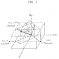
- Fig. 1 is an explanatory diagram for explaining plane orientation of the single crystal wafer of the present invention.
- Fig. 2 shows an exemplary apparatus utilizing a radial line slot antenna for forming an oxide film on the single crystal wafer of the present invention.
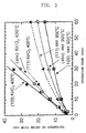
- Fig. 3 is a graph showing a relationship between oxide film thickness containing Kr and oxidation time during oxidation of silicon wafer surface using Kr/O 2 high density plasma.
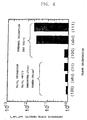
- Fig. 4 is a graph showing the results of low frequency C-V measurement for interface state density of oxide film.
- the inventors of the present invention noted the relationship between the plane orientation and likeliness of breakage of wafer in order to utilize the technique. That is, since it became unnecessary to limit the plane orientation for the device characteristics, they conceived that, if a plane orientation providing strength as high as possible was selected, wafers causing breakage or chipping at a level comparable to those attained by conventional wafers could be obtained even if the wafers were produced with a smaller thickness compared with those of the conventional wafers, and as a result, number of wafers obtainable from one ingot could be increased.
- Japanese Patent Laid-open Publication No. 9-262825 discloses that, as for the relationship between the plane orientation and likeliness of breakage of wafer, when a single crystal is sliced with a wire saw, wafers are likely to suffer from breakage if a saw mark conforms to the cleavage direction.
- the cleavage plane considered in this reference is only the ⁇ 110 ⁇ plane orthogonal to the ⁇ 100 ⁇ plane, and the ⁇ 110 ⁇ plane having an angle of 45° with respect to the ⁇ 100 ⁇ plane is not considered at all.
- all the sliced wafers are wafers having a low index plane such as ⁇ 100 ⁇ plane.
- the inventors of the present invention conceived that, in order to produce a wafer unlikely to break, consideration of only the ⁇ 110 ⁇ plane perpendicular to the ⁇ 100 ⁇ plane was insufficient, and it was necessary to consider the ⁇ 110 ⁇ plane having an angle of 45° with respect to the ⁇ 100 ⁇ plane. Thus, the present invention was accomplished.
- Fig. 1 is a diagram for explaining plane orientation of the single crystal wafer of the present invention.
- the arrowhead (vector) represented by the bold line in Fig. 1 indicates the plane orientation of the single crystal wafer of the present invention (orientation of the normal of the wafer surface). It has, with respect to the [100] axis (X-axis), tilting angles of ⁇ (0° ⁇ ⁇ ⁇ 90°) for the [011] direction, ⁇ (0° ⁇ ⁇ ⁇ 90°) for the [01-1] direction and ⁇ (0° ⁇ ⁇ ⁇ 45°) for the [10-1] direction.
- the single crystal wafer having this plane orientation will have a plane tilting by angles of ⁇ , ⁇ and ⁇ from the cleavage planes, (011) plane, (01-1) plane and (10-1) plane, respectively, and thus mechanical strength of the wafer with respect to an external stress is increased compared with conventional wafers having a low index plane orientation.
- the numbers of effective bonds in the case of silicon single crystal are 11.8 x 10 14 numbers/cm 2 , 9.6 x 10 14 numbers/cm 2 and 6.8 x 10 14 numbers/cm 2 for the (111), (110) and (100) planes, respectively.
- ⁇ does not mean an tilting angle for the [10-1] direction shown in Fig. 1, but means a tilting angle for the [101] direction.
- a single crystal ingot produced under ordinary condition can be sliced with a predetermined angle.
- ingots ordinarily produced have a crystal orientation of ⁇ 100> or ⁇ 111>, and ⁇ 110> and ⁇ 511> are known as crystal orientations that enable crystal production without causing unacceptable deformation of crystal.
- a seed crystal preliminarily provided with an off angle of several degrees or so as a seed crystal used at the time of pulling a single crystal a crystal having an off angle can be pulled. Therefore, by using such a crystal, adjustment of the orientation at the time of slicing can also be simplified.
- the surface of the single crystal wafer of the present invention described above has a plane orientation tilting from all of the ⁇ 110 ⁇ planes along which cleavage is likely to occur, a wafer that is more unlikely to break with an external stress and has a smaller thickness compared with conventional wafers having ⁇ 100 ⁇ planes can be produced.
- the thickness can be made thinner than the above, and it is also possible to obtain a thickness of less than 600 ⁇ m in the case of a silicon wafer having a diameter of 200 mm, for example. Therefore, number of wafers that can be produced from one single crystal ingot is increased, and it becomes possible to reduce the production cost.
- an insulator film having characteristics as a gate insulator film comparable to those of conventional films and showing no dependency on the plane orientation can surely be formed.
- Fig. 2 shows an exemplary apparatus utilizing a radial line slot antenna for forming an oxide film on the single crystal wafer of the present invention.
- This embodiment has a novel characteristic that Kr is used as plasma excitation gas for the oxide film formation.
- Kr gas and O 2 gas are introduced from a shower plate 2 to adjust the pressure in the processing chamber to be about 1 Torr (about 133 Pa).
- a circular substrate 3 such as a silicon wafer is placed on a sample stand 4 having a heating mechanism, and temperature is adjusted so that the temperature of the sample should become 400°C. This temperature may be in the range of 200 to 550°C.
- a microwave of 2.45 GHz is supplied to the processing chamber via a radial line slot antenna 6 and a dielectric plate 7 to generate high density plasma in the processing chamber. Further, any frequency of the supplied microwave may be selected so long as it is in the range of 900 MHz to 10 GHz.
- a spacing between the shower plate 2 and the substrate 3 is adjusted to 6 cm in this embodiment.
- a narrower spacing enables film formation with a higher rate.
- a microwave may be introduced into the processing chamber by using another method.
- the substrate surface is oxidized with this atomic oxygen.
- the conventional oxidation of silicon surface is attained by H 2 O molecules and/or O 2 molecules, and the treatment temperature is extremely high, i.e., 800°C or higher.
- the oxidation by atomic oxygen according to the present invention may be realized at a sufficiently low temperature, i.e., 550°C or lower.
- the inventors of the present invention measured thickness of oxide film grown by oxidation treatment of 10 minutes at a silicon substrate temperature of 400°C with keeping pressure ratios of 97% for Kr and 3% for oxygen in the processing chamber and a varying gas pressure in the processing chamber. As a result, the thickness of oxide film became the largest when the gas pressure in the processing chamber was 1 Torr, and thus it was found that oxidation condition of that pressure or pressure around that was preferred. It was found that this pressure condition was similarly preferred for the (abc) plane as well as the (100) plane and the (111) plane.
- Fig. 3 shows a relationship between oxide film thickness containing Kr and oxidation time during oxidation of silicon wafer surface using Kr/O 2 high density plasma.
- the graph shows the results for silicon substrates having a plane orientation of (100) plane, (111) plane or (abc) plane.
- Fig. 3 also shows oxidation time dependency in conventional dry thermal oxidation at 900°C. It is evident that the oxidation rate in the Kr/O 2 high density plasma oxidation at a substrate temperature of 400°C and a processing chamber pressure of 1 Torr is higher than the oxidation rate in the dry O 2 oxidation at a substrate temperature of 900°C and atmospheric pressure.
- the productivity of surface oxidation technique can also be markedly improved.
- O 2 molecules or H 2 O molecules pass through an oxide film formed on a surface by diffusion and reach the interface of silicon/silicon oxide film to contribute to the oxidation. Therefore, it is a common knowledge that the oxidation rate is rate-determined by the diffusion rates of O 2 molecules or H 2 O molecules through the oxide film, and it increases with a factor of t 1/2 as a function of oxidation time t.
- the oxidation rate is linear until the oxide film thickness reaches 35 nm. This means that the diffusion rate of atomic oxygen in the silicon oxide film is extremely high, and atomic oxygen can freely pass through the silicon oxide film.
- Kr density distribution along the depth direction in a silicon oxide film formed by the aforementioned procedure was investigated by using a total reflection X-ray fluorescence spectrophotometer.
- Kr density decreased in a region having a thinner oxide film thickness, and Kr existed at a density of about 2 x 10 11 cm -2 at a silicon oxide film surface. That is, in this silicon film, the Kr concentration in the film is constant for the film thickness of 4 nm or more, and the Kr concentration decreases towards the silicon/silicon oxide film interface.
- Fig. 4 shows the results of low frequency C-V measurement for interface state density of an oxide film.
- the silicon oxide film was formed at a substrate temperature of 400°C by using the apparatus shown in Fig. 2.
- the partial pressure of oxygen in rare gas was fixed to 3%, and the pressure in the processing chamber was fixed to 1 Torr.
- the interface state density of a thermal oxide film formed at 900°C in an atmosphere of 100% oxygen is also shown.
- the interface state density of the oxide film formed by using Kr gas was low for all of the (100) plane, (111) plane and (abc) plane and equivalent to the interface state density of the thermal oxide film formed at 900°C in a dry oxidation atmosphere so as to have a (100) plane.
- the interface state density of the thermal oxide film formed with the (111) plane is larger by 1 digit order compared with them.
- the interface state density referred to in the present invention means interface trap density (Dit) in the mid gap, and it is obtained by the quasi-static C-V technique (quasi-static capacitance-voltage technique) .
- the oxide film obtained by the silicon substrate surface oxidation using Kr/O 2 high density plasma showed favorable characteristics comparable to those obtained for the oxide film obtained by the thermal oxidation at 900°C.
- the oxide film grown with the Kr/O 2 high density plasma was oxidized at a low temperature of 400°C, it showed characteristics comparable to or superior to those shown by the conventional oxide film of a (100) plane obtained by the high temperature thermal oxidation, even for the (abc) plane, without being influenced by the plane orientation.
- Kr contained in the oxide film It is considered that when Kr is contained in the oxide film, stress in the film or at the Si/SiO 2 interface is relaxed, charges in the film and the interface state density are reduced, and thereby the electric characteristics of the silicon oxide film are markedly improved. It is considered that, in particular, Kr contained at a level of 5 x 10 11 cm -2 or less in the concentration of the surface contributes to the improvements of the electric characteristics and reliability characteristics of the silicon oxide film.
- the MIS transistor utilizing this gate oxide film shows favorable characteristics in any plane orientation, and characteristics equivalent to those obtained with the (100) plane can be obtained even with the (abc) plane.
- an apparatus for plasma process that enables low temperature oxide film formation using plasma may also be used.
- an oxide film can also be formed by a two-stage shower plate type plasma process apparatus having first gas discharging means for discharging Kr gas for exciting plasma by a microwave and second gas discharging means for discharging oxygen gas, which is different from the first gas discharging means.
- a nitride film forming apparatus is almost the same as the apparatus shown in Fig. 2.
- Ar or Kr is used as plasma excitation gas for the nitride film formation.
- Inside of the vacuum chamber (processing chamber) 1 is made vacuum, and Ar gas and NH 3 gas are introduced from the shower plate 2 to adjust the pressure in the processing chamber to be about 100 mTorr.
- a circular substrate 3 such as a silicon wafer is placed on the sample stand 4 having a heating mechanism, and temperature is adjusted so that the temperature of the sample should become 500°C. This temperature may be adjusted to be in the range of about 200 to 550°C.
- a microwave of 2.45 GHz is supplied to the processing chamber via the radial line slot antenna 6 and the dielectric plate 7 to generate high density plasma in the processing chamber.
- the frequency of the supplied microwave may be in the range of 900 MHz to 10 GHz.
- a spacing between the shower plate 2 and the substrate 3 is adjusted to 6 cm in this example. A narrower spacing enables film formation with a higher rate.
- a microwave may be introduced into the processing chamber by using another method.
- Ar is used as the plasma excitation gas
- Kr can also provide similar results.
- NH 3 is used as the plasma process gas
- a mixed gas of N 2 and H 2 or the like may also be used.
- NH* radicals are efficiently generated by Ar* or Kr* in an intermediate excited state.
- the substrate surface is nitrided.
- Such nitriding of silicon enables formation of nitride film of high quality at a low temperature without limitation of the plane orientation of silicon.
- one of the important requirements is the presence of hydrogen.
- hydrogen exists in the plasma, dangling bonds in the silicon nitride film or at the interface form Si-H and N-H bonds to cause termination, and as a result, electronic traps in the silicon nitride film and at the interface are eliminated.
- the presence of the Si-H bonds and N-H bonds in the nitride film of the present invention has been confirmed by infrared absorption spectrometry and X-ray photoelectron spectrometry of the film.
- the presence of hydrogen also eliminates the hysteresis of CV characteristics and suppresses the silicon/silicon nitride interface state density as low as 3 x 10 10 eV -1 cm -2 .
- a rare gas Ar or Kr
- a mixed gas of N 2 /H 2 if the hydrogen gas is used at a partial pressure of 0.5% or more, electron and hole traps in the film are sharply decreased.
- Relative dielectric constant of the silicon nitride film of this embodiment was 7.9, which is twice as large as that of the silicon oxide film.
- the nitride film of the present invention can also be used.
- the nitride film can also be formed by a two-stage shower plate type plasma process apparatus having first gas discharging means for discharging Ar or Kr gas for exciting plasma by a microwave and second gas discharging means for discharging NH 3 (or N 2 /H 2 gas) gas, which is different from the first gas discharging means.
- a silicon wafer having an (abc) plane as the main surface shows high mechanical strength. Therefore, it becomes possible to slice a silicon single crystal ingot for solar cells with a thickness smaller than the thickness used in the slicing of conventional silicon single crystal ingot for solar cells (about 400 to 600 ⁇ m for a diameter of 100 to 150 mm), and the thickness can be, for example, 300 to 450 ⁇ m or less than the foregoing range for a diameter of 100 to 150 mm. Therefore, the yield of wafers is improved for the thickness made thinner, and thus it becomes possible to reduce the cost.
- the slicing is performed by using a wire saw or an inner diameter slicer, and damage is generated in a crystal by mechanical impact at the time of the slicing. Such damage degrades electric characteristics of wafers and also affect characteristic of the cell. Therefore, in order to eliminate such a damage layer, chemical etching is performed for about 10 to 20 ⁇ m. Such etching is usually performed by using a mixed acid of HF and HNO 3 , and several tens of wafers are put into a carrier for etching to perform the etching with rotating the carrier in order to attain uniform etching over the surfaces. Therefore, higher wafer strength is advantageous for such an etching process, since wafers are unlikely to break even with a small thickness. Further, etching with an alkali for increasing conversion efficiency, called texture treatment, is also performed.
- n-type impurities are diffused in the wafer to form a pn junction, and the wafer is subjected to formation of electrodes and formation of antireflection film to produce a solar cell.
- a conversion efficiency of 20% or more and an output voltage of 1.5 V can be attained.
- the wafer of the present invention having the (abc) plane as the main surface can sufficiently bear the production steps of devices and solar cells even with a smaller thickness, and thus it enables marked reduction of the production cost.
Landscapes
- Chemical & Material Sciences (AREA)
- Engineering & Computer Science (AREA)
- Crystallography & Structural Chemistry (AREA)
- Materials Engineering (AREA)
- Metallurgy (AREA)
- Organic Chemistry (AREA)
- Formation Of Insulating Films (AREA)
- Crystals, And After-Treatments Of Crystals (AREA)
- Photovoltaic Devices (AREA)
- Insulated Gate Type Field-Effect Transistor (AREA)
Abstract
Description
Claims (7)
- A single crystal wafer, wherein the main surface has a plane or a plane equivalent to a plane tilting with respect to a [100] axis of single crystal by angles of α (0° < α < 90°) for the [011] direction, β (0° < β < 90°) for the [01-1] direction and γ (0° ≦ γ < 45°) for the [10-1] or [101] direction.
- The single crystal wafer according to Claim 1, which consists of semiconductor silicon.
- The single crystal wafer according to Claim 1 or 2, which satisfies a relationship of thickness of wafer (µm)/diameter of wafer (mm) ≦ 3.
- A single crystal wafer, wherein an insulator film is formed on a surface of the single crystal wafer according to Claim 2 or 3.
- The single crystal wafer according to Claim 4, wherein the insulator film is a silicon oxide film containing Kr.
- The single crystal wafer according to Claim 4, wherein the insulator film is a silicon nitride film containing Ar or Kr and hydrogen.
- A solar cell produced by using the single crystal wafer according to any one of Claims 1 to 6.
Applications Claiming Priority (3)
| Application Number | Priority Date | Filing Date | Title |
|---|---|---|---|
| JP2000208870 | 2000-07-10 | ||
| JP2000208870A JP3910004B2 (en) | 2000-07-10 | 2000-07-10 | Semiconductor silicon single crystal wafer |
| PCT/JP2001/005892 WO2002005335A1 (en) | 2000-07-10 | 2001-07-06 | Single crystal wafer and solar battery cell |
Publications (3)
| Publication Number | Publication Date |
|---|---|
| EP1302976A1 true EP1302976A1 (en) | 2003-04-16 |
| EP1302976A4 EP1302976A4 (en) | 2007-09-12 |
| EP1302976B1 EP1302976B1 (en) | 2009-07-15 |
Family
ID=18705372
Family Applications (1)
| Application Number | Title | Priority Date | Filing Date |
|---|---|---|---|
| EP01947892A Expired - Lifetime EP1302976B1 (en) | 2000-07-10 | 2001-07-06 | Single crystal wafer and solar battery cell |
Country Status (9)
| Country | Link |
|---|---|
| US (1) | US7459720B2 (en) |
| EP (1) | EP1302976B1 (en) |
| JP (1) | JP3910004B2 (en) |
| KR (1) | KR100804247B1 (en) |
| CN (1) | CN1217380C (en) |
| AU (2) | AU2001269469B2 (en) |
| DE (1) | DE60139258D1 (en) |
| TW (1) | TW527635B (en) |
| WO (1) | WO2002005335A1 (en) |
Families Citing this family (12)
| Publication number | Priority date | Publication date | Assignee | Title |
|---|---|---|---|---|
| JPWO2003056622A1 (en) * | 2001-12-26 | 2005-05-12 | 東京エレクトロン株式会社 | Substrate processing method and semiconductor device manufacturing method |
| JP2003257984A (en) * | 2002-03-05 | 2003-09-12 | Sumitomo Mitsubishi Silicon Corp | Silicon wafer and its manufacturing method |
| JP2004319909A (en) * | 2003-04-18 | 2004-11-11 | Tadahiro Omi | Electron beam exposure mask and method of manufacturing the same |
| JP4407188B2 (en) | 2003-07-23 | 2010-02-03 | 信越半導体株式会社 | Silicon wafer manufacturing method and silicon wafer |
| JP5124189B2 (en) * | 2007-07-11 | 2013-01-23 | シャープ株式会社 | Method for manufacturing photoelectric conversion element |
| JP2010251667A (en) * | 2009-04-20 | 2010-11-04 | Sanyo Electric Co Ltd | Solar cell |
| JP5485060B2 (en) * | 2010-07-28 | 2014-05-07 | 三洋電機株式会社 | Manufacturing method of solar cell |
| JP6091108B2 (en) * | 2012-08-03 | 2017-03-08 | アズビル株式会社 | Silicon tube manufacturing method |
| JP6502399B2 (en) | 2017-02-06 | 2019-04-17 | Jx金属株式会社 | Single crystal silicon sputtering target |
| JP6546953B2 (en) | 2017-03-31 | 2019-07-17 | Jx金属株式会社 | Sputtering target-backing plate assembly and method for manufacturing the same |
| CN111364097A (en) * | 2020-04-15 | 2020-07-03 | 晶科能源有限公司 | Monocrystalline silicon seed crystal, silicon ingot, silicon block and silicon wafer of directionally solidified ingot casting, and preparation method and application thereof |
| DE102020209092A1 (en) * | 2020-07-21 | 2022-01-27 | Sicrystal Gmbh | Crystal structure orientation in semiconductor semi-finished products and semiconductor substrates to reduce cracks and method for adjusting them |
Family Cites Families (35)
| Publication number | Priority date | Publication date | Assignee | Title |
|---|---|---|---|---|
| US3925107A (en) * | 1974-11-11 | 1975-12-09 | Ibm | Method of stabilizing mos devices |
| JPS5389367A (en) | 1977-01-18 | 1978-08-05 | Hitachi Cable Ltd | Substrate crystal for semiconductor epitaxial growth |
| US4255212A (en) * | 1979-07-02 | 1981-03-10 | The Regents Of The University Of California | Method of fabricating photovoltaic cells |
| JPS56109896A (en) | 1980-02-01 | 1981-08-31 | Hitachi Ltd | Semiconductor single crystal and its growing method |
| JPS58128775A (en) * | 1982-01-28 | 1983-08-01 | Toshiba Corp | Solar cell and its manufacture |
| JPS6265996A (en) | 1985-09-18 | 1987-03-25 | Toshiba Corp | Production of compound semiconductor crystal |
| JPS62226891A (en) | 1986-03-28 | 1987-10-05 | Shin Etsu Handotai Co Ltd | Substrate for semiconductor device |
| US4824489A (en) * | 1988-02-02 | 1989-04-25 | Sera Solar Corporation | Ultra-thin solar cell and method |
| JPH02180796A (en) | 1988-12-29 | 1990-07-13 | Sharp Corp | Production of silicon carbide single crystal |
| JPH02133926A (en) | 1988-11-15 | 1990-05-23 | Sanyo Electric Co Ltd | Manufacture of semiconductor device |
| JPH0355822A (en) * | 1989-07-25 | 1991-03-11 | Shin Etsu Handotai Co Ltd | Manufacture of substrate for forming semiconductor element |
| JPH0361634A (en) | 1989-07-27 | 1991-03-18 | Honda Motor Co Ltd | Automotive engine control valve control method |
| US5067985A (en) * | 1990-06-08 | 1991-11-26 | The United States Of America As Represented By The Secretary Of The Air Force | Back-contact vertical-junction solar cell and method |
| JPH08760B2 (en) * | 1991-03-14 | 1996-01-10 | 信越半導体株式会社 | Quality inspection method for silicon wafers |
| JPH0590117A (en) * | 1991-09-27 | 1993-04-09 | Toshiba Corp | Single crystal thin film semiconductor device |
| JPH05343321A (en) | 1992-06-08 | 1993-12-24 | Nippon Telegr & Teleph Corp <Ntt> | Compound semiconductor substrate and manufacturing method thereof |
| JP3081706B2 (en) * | 1992-06-12 | 2000-08-28 | 株式会社東芝 | Substrate for semiconductor device |
| JPH06265996A (en) * | 1993-03-12 | 1994-09-22 | Canon Inc | Camera |
| JP3634400B2 (en) * | 1994-04-18 | 2005-03-30 | セイコーエプソン株式会社 | Balloon fluid discharge device and method for manufacturing the same |
| JP2789301B2 (en) | 1994-07-21 | 1998-08-20 | 住友シチックス株式会社 | Semiconductor substrate and manufacturing method thereof |
| JPH0888272A (en) * | 1994-09-19 | 1996-04-02 | Shin Etsu Handotai Co Ltd | Method for manufacturing substrate for semiconductor integrated circuit |
| DE19611043B4 (en) * | 1995-03-20 | 2006-02-16 | Toshiba Ceramics Co., Ltd. | A method of producing a silicon wafer, a method of forming a silicon wafer, and a method of manufacturing a semiconductor device |
| CN1089486C (en) * | 1995-06-26 | 2002-08-21 | 精工爱普生株式会社 | Method for forming crystalline semiconductor film |
| JP3397968B2 (en) | 1996-03-29 | 2003-04-21 | 信越半導体株式会社 | Slicing method of semiconductor single crystal ingot |
| JP3351679B2 (en) * | 1996-05-22 | 2002-12-03 | 株式会社リコー | Method for manufacturing polycrystalline silicon thin film laminate and silicon thin film solar cell |
| JP3813740B2 (en) * | 1997-07-11 | 2006-08-23 | Tdk株式会社 | Substrates for electronic devices |
| FR2769640B1 (en) * | 1997-10-15 | 1999-12-17 | Sgs Thomson Microelectronics | IMPROVING THE MECHANICAL STRENGTH OF A MONOCRYSTALLINE SILICON WAFER |
| JPH11162859A (en) * | 1997-11-28 | 1999-06-18 | Canon Inc | Liquid crystal growth method of silicon crystal and method of manufacturing solar cell using the same |
| JPH11162973A (en) * | 1997-11-28 | 1999-06-18 | Nec Corp | Method for manufacturing semiconductor device |
| JP2000150512A (en) * | 1998-04-06 | 2000-05-30 | Tadahiro Omi | Silicon nitride film, formation method therefor, and semiconductor device |
| JP3456143B2 (en) * | 1998-05-01 | 2003-10-14 | 信越半導体株式会社 | Laminated materials and optical functional devices |
| JP3255114B2 (en) * | 1998-06-18 | 2002-02-12 | 信越半導体株式会社 | Method for producing nitrogen-doped low defect silicon single crystal |
| JP4397491B2 (en) * | 1999-11-30 | 2010-01-13 | 財団法人国際科学振興財団 | Semiconductor device using silicon having 111 plane orientation on surface and method of forming the same |
| JP4084916B2 (en) * | 2000-06-21 | 2008-04-30 | 株式会社東洋新薬 | Antihypertensive food containing raw material derived from wheat |
| DE10047346B4 (en) * | 2000-09-25 | 2007-07-12 | Mitsubishi Materials Silicon Corp. | Method for producing a silicon wafer for depositing an epitaxial layer and epitaxial wafer |
-
2000
- 2000-07-10 JP JP2000208870A patent/JP3910004B2/en not_active Expired - Fee Related
-
2001
- 2001-07-06 AU AU2001269469A patent/AU2001269469B2/en not_active Expired
- 2001-07-06 DE DE60139258T patent/DE60139258D1/en not_active Expired - Lifetime
- 2001-07-06 US US10/332,434 patent/US7459720B2/en not_active Expired - Lifetime
- 2001-07-06 EP EP01947892A patent/EP1302976B1/en not_active Expired - Lifetime
- 2001-07-06 AU AU6946901A patent/AU6946901A/en active Pending
- 2001-07-06 WO PCT/JP2001/005892 patent/WO2002005335A1/en not_active Ceased
- 2001-07-06 CN CN018124992A patent/CN1217380C/en not_active Expired - Lifetime
- 2001-07-06 KR KR1020037000322A patent/KR100804247B1/en not_active Expired - Fee Related
- 2001-07-09 TW TW090116779A patent/TW527635B/en not_active IP Right Cessation
Also Published As
| Publication number | Publication date |
|---|---|
| US20030160304A1 (en) | 2003-08-28 |
| DE60139258D1 (en) | 2009-08-27 |
| CN1217380C (en) | 2005-08-31 |
| KR20030026969A (en) | 2003-04-03 |
| EP1302976A4 (en) | 2007-09-12 |
| JP3910004B2 (en) | 2007-04-25 |
| AU6946901A (en) | 2002-01-21 |
| KR100804247B1 (en) | 2008-02-20 |
| WO2002005335A1 (en) | 2002-01-17 |
| AU2001269469B2 (en) | 2006-11-02 |
| EP1302976B1 (en) | 2009-07-15 |
| CN1440565A (en) | 2003-09-03 |
| TW527635B (en) | 2003-04-11 |
| JP2002025874A (en) | 2002-01-25 |
| US7459720B2 (en) | 2008-12-02 |
Similar Documents
| Publication | Publication Date | Title |
|---|---|---|
| Fletcher et al. | GaAs light‐emitting diodes fabricated on Ge‐coated Si substrates | |
| EP0887843B1 (en) | Method of manufacturing a transistor with a silicon-germanium gate | |
| KR100352368B1 (en) | Semiconductor substrate and method for producing the same | |
| US5773355A (en) | Method for manufacturing semiconductor substrate | |
| EP0779666A2 (en) | Semiconductor device and method of fabricating semiconductor device | |
| US7459720B2 (en) | Single crystal wafer and solar battery cell | |
| US6995077B2 (en) | Epitaxially coated semiconductor wafer and process for producing it | |
| US20200126847A1 (en) | High resistivity silicon-on-insulator substrate having enhanced charge trapping efficiency | |
| US4435447A (en) | Method for forming an insulating film on a semiconductor substrate surface | |
| Wong et al. | The poly‐single crystalline silicon interface | |
| EP1130634B1 (en) | Semiconductor device and method for forming silicon oxide film | |
| EP0510858A1 (en) | Method of selectively forming a TiNx layer by MOCVD, on a semi-conductor device | |
| US20240258155A1 (en) | Methods of manufacturing semiconductor-on-insulator wafers having charge trapping layers with controlled stress | |
| JPH1064917A (en) | Silicon wafer and manufacturing method thereof | |
| US7122865B2 (en) | SOI wafer and process for producing it | |
| EP3993018B1 (en) | Method of manufacture of a semiconductor on insulator structure | |
| US5548136A (en) | Substrate with a compound semiconductor surface layer and method for preparing the same | |
| US5970365A (en) | Silicon wafer including amorphous silicon layer formed by PCVD and method of manufacturing wafer | |
| EP4407657A1 (en) | Nitride semiconductor substrate and method for producing same | |
| Rogers et al. | Low‐temperature homoepitaxial growth of Si by electron cyclotron resonance plasma enhanced chemical vapor deposition | |
| JP2560038B2 (en) | Method for manufacturing semiconductor device | |
| KR100676521B1 (en) | Low temperature oxide back seal forming method and wafer manufactured using the same | |
| JPH1197439A (en) | Semiconductor device and manufacturing method thereof | |
| Copel et al. | IBM-TJ Watson Research Center, Yorktown Heights., NY 10598, USA* IBM East Fishkill, Hopewell Jct., NY 12533, USA Silicon (oxy) nitride films used in the semiconductor fabrication process continue to be | |
| Copel | CP D'Emic, EP Gusev, K. Chan, T. Zabel, M. Copel, R. Murphy*, P. Kozlowski, J. Newbury IBM-TJ Watson Research Center, Yorktown Heights., NY 10598, USA* IBM East Fishkill, Hopewell Jct., NY 12533, USA Silicon (oxy) nitride films used in the semiconductor fabrication process continue to be |
Legal Events
| Date | Code | Title | Description |
|---|---|---|---|
| PUAI | Public reference made under article 153(3) epc to a published international application that has entered the european phase |
Free format text: ORIGINAL CODE: 0009012 |
|
| 17P | Request for examination filed |
Effective date: 20030123 |
|
| AK | Designated contracting states |
Designated state(s): AT BE CH CY DE DK ES FI FR GB GR IE IT LI LU MC NL PT SE TR |
|
| RBV | Designated contracting states (corrected) |
Designated state(s): AT BE CH CY DE FR GB IT LI NL |
|
| A4 | Supplementary search report drawn up and despatched |
Effective date: 20070814 |
|
| 17Q | First examination report despatched |
Effective date: 20080304 |
|
| GRAP | Despatch of communication of intention to grant a patent |
Free format text: ORIGINAL CODE: EPIDOSNIGR1 |
|
| RBV | Designated contracting states (corrected) |
Designated state(s): DE FR GB IT NL |
|
| RAP1 | Party data changed (applicant data changed or rights of an application transferred) |
Owner name: SHIN-ETSU HANDOTAI CO., LTD. |
|
| GRAS | Grant fee paid |
Free format text: ORIGINAL CODE: EPIDOSNIGR3 |
|
| GRAA | (expected) grant |
Free format text: ORIGINAL CODE: 0009210 |
|
| AK | Designated contracting states |
Kind code of ref document: B1 Designated state(s): DE FR GB IT NL |
|
| REG | Reference to a national code |
Ref country code: GB Ref legal event code: FG4D |
|
| REF | Corresponds to: |
Ref document number: 60139258 Country of ref document: DE Date of ref document: 20090827 Kind code of ref document: P |
|
| PLBE | No opposition filed within time limit |
Free format text: ORIGINAL CODE: 0009261 |
|
| STAA | Information on the status of an ep patent application or granted ep patent |
Free format text: STATUS: NO OPPOSITION FILED WITHIN TIME LIMIT |
|
| 26N | No opposition filed |
Effective date: 20100416 |
|
| PG25 | Lapsed in a contracting state [announced via postgrant information from national office to epo] |
Ref country code: IT Free format text: LAPSE BECAUSE OF FAILURE TO SUBMIT A TRANSLATION OF THE DESCRIPTION OR TO PAY THE FEE WITHIN THE PRESCRIBED TIME-LIMIT Effective date: 20090715 |
|
| REG | Reference to a national code |
Ref country code: FR Ref legal event code: PLFP Year of fee payment: 16 |
|
| REG | Reference to a national code |
Ref country code: FR Ref legal event code: PLFP Year of fee payment: 17 |
|
| REG | Reference to a national code |
Ref country code: FR Ref legal event code: PLFP Year of fee payment: 18 |
|
| PGFP | Annual fee paid to national office [announced via postgrant information from national office to epo] |
Ref country code: FR Payment date: 20200611 Year of fee payment: 20 |
|
| PGFP | Annual fee paid to national office [announced via postgrant information from national office to epo] |
Ref country code: GB Payment date: 20200624 Year of fee payment: 20 Ref country code: NL Payment date: 20200615 Year of fee payment: 20 |
|
| PGFP | Annual fee paid to national office [announced via postgrant information from national office to epo] |
Ref country code: DE Payment date: 20200624 Year of fee payment: 20 |
|
| REG | Reference to a national code |
Ref country code: DE Ref legal event code: R071 Ref document number: 60139258 Country of ref document: DE |
|
| REG | Reference to a national code |
Ref country code: NL Ref legal event code: MK Effective date: 20210705 |
|
| REG | Reference to a national code |
Ref country code: GB Ref legal event code: PE20 Expiry date: 20210705 |
|
| PG25 | Lapsed in a contracting state [announced via postgrant information from national office to epo] |
Ref country code: GB Free format text: LAPSE BECAUSE OF EXPIRATION OF PROTECTION Effective date: 20210705 |