EP1302972A2 - Method and scanning electron microscope for measuring width of material on sample - Google Patents
Method and scanning electron microscope for measuring width of material on sample Download PDFInfo
- Publication number
- EP1302972A2 EP1302972A2 EP02021294A EP02021294A EP1302972A2 EP 1302972 A2 EP1302972 A2 EP 1302972A2 EP 02021294 A EP02021294 A EP 02021294A EP 02021294 A EP02021294 A EP 02021294A EP 1302972 A2 EP1302972 A2 EP 1302972A2
- Authority
- EP
- European Patent Office
- Prior art keywords
- width
- sample
- measured
- dimension
- value
- Prior art date
- Legal status (The legal status is an assumption and is not a legal conclusion. Google has not performed a legal analysis and makes no representation as to the accuracy of the status listed.)
- Withdrawn
Links
Images




Classifications
-
- G—PHYSICS
- G01—MEASURING; TESTING
- G01B—MEASURING LENGTH, THICKNESS OR SIMILAR LINEAR DIMENSIONS; MEASURING ANGLES; MEASURING AREAS; MEASURING IRREGULARITIES OF SURFACES OR CONTOURS
- G01B15/00—Measuring arrangements characterised by the use of electromagnetic waves or particle radiation, e.g. by the use of microwaves, X-rays, gamma rays or electrons
-
- H—ELECTRICITY
- H01—ELECTRIC ELEMENTS
- H01J—ELECTRIC DISCHARGE TUBES OR DISCHARGE LAMPS
- H01J37/00—Discharge tubes with provision for introducing objects or material to be exposed to the discharge, e.g. for the purpose of examination or processing thereof
- H01J37/26—Electron or ion microscopes; Electron or ion diffraction tubes
- H01J37/28—Electron or ion microscopes; Electron or ion diffraction tubes with scanning beams
-
- H—ELECTRICITY
- H01—ELECTRIC ELEMENTS
- H01J—ELECTRIC DISCHARGE TUBES OR DISCHARGE LAMPS
- H01J2237/00—Discharge tubes exposing object to beam, e.g. for analysis treatment, etching, imaging
- H01J2237/26—Electron or ion microscopes
- H01J2237/28—Scanning microscopes
- H01J2237/2813—Scanning microscopes characterised by the application
- H01J2237/2814—Measurement of surface topography
Definitions
- the present invention relates to a method and a system for when measuring the dimension of a fine pattern shape of an LSI or the like, measuring the dimension of an object to be width-measured with accuracy.
- a cursor is adjusted to either a luminance leading part or a luminance trailing part of an object to be measured either on the secondary electron image or on the reflected electron image and the dimension between both sides of the cursor is, as a result, decided as the dimension of the object to be measured.
- JP-A-6-347246 an electron beam is applied to an object to be measured while scanning the object with the electron beam being applied, and a sample image is formed depending on a quantity of secondary electrons and reflected electrons which have been emitted and generated therefrom, respectively, to measure the width of the object.
- the diameter of the applied electron beam e.g., several nano meters
- the diameter of the applied electron beam is so large as to be non-negligible against the size of such semiconductor devices.
- the present invention has been made in order to solve the above-mentioned problems associated with the prior art, and it is, therefore, an object of the present invention to provide a method and a scanning electron microscope for measuring a width of an object on a sample which are capable of reducing or removing an error in width measurement resulting from the influence of the dimension of an electron beam diameter to obtain an accurate value of a measured width.
- a method of measuring a width of an object on a sample in which the sample is scanned with a beam to measure the width of an object to be width-measured on the sample on the basis of a secondary signal obtained from the sample wherein the width-measured value of the object of the width measurement obtained on the basis of the secondary signal is corrected with a value with respect to a dimension value of the beam diameter.
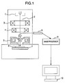
- Fig. 1 is a schematic cross sectional view, partly in block diagram, showing construction of a scanning electron microscope according to an embodiment of the present invention.
- a suitable voltage is applied from a high-voltage control power source which is controlled by a microprocessor (CPU (not shown)) to an electrode gun 1, and an electron beam 2 is drawn from the electrode gun 1 with a predetermined emission current.
- the electron beam 2 is then condensed by an electromagnetic lens 3 which is controlled by a lens control power source (not shown) to be applied in the form of a small spot onto a sample 6 through an objective lens 5 which is similarly controlled by the lens control power source.
- the various forms such as the in-lens system in which a sample is arranged between magnetic poles, the out-lens system in which a sample is arranged at the height different from that of objective lens magnetic poles, or the snorkel system (semi-in-lens system).
- the retarding system in which a magnetic voltage is applied onto a sample to decelerate a primary electron beam may also be adopted.
- each of the various lenses may be constructed by the electrostatic type lens which is constituted by a plurality of electrodes.
- an acceleration cylinder to which a positive voltage is applied may be provided.
- the sample 6 which is arranged on a sample holder 7 is scanned through a deflecting lens 4 with the electron beam 2 either in a two-dimensional manner or in a three-dimensional manner containing the direction of application of the electron beam.
- the sample holder 7 is arranged on a sample stage (not shown) and is provided with the function of being moved to move the sample 6 in a direction (X - Y direction) perpendicular to an optical axis of the electron beam 2.
- the present invention is not intended to be limited thereto. For example, there may be added a rotation function of rotating the sample 6 or the inclination function of inclining the sample with respect to the optical axis of the electron beam 2.
- a secondary signal obtained from the secondary electrons, the reflected electrons and the like which have been respectively emitted from the sample 6 through the application of the electron beam 2 onto the sample 6 is detected by a secondary electron detector 8.
- the secondary signal detected by the secondary electron detector 8 has been amplified by a signal amplifier (not shown), it is transferred to an image processor 9 to be displayed in the form of a sample image on an image display monitor 10.
- the various kinds of operation buttons through which instructions for the setting of the electronic optical system, the setting of the scanning conditions and the like are issued can be displayed in addition to the sample image on the image display monitor 10.
- the system according to the present embodiment of the invention is provided with the function of forming and displaying a beam profile on the basis of either a quantity of generated secondary electrons, or luminance information of the sample image displayed on the image display monitor 10.
- the width-measurement for a pattern of a semiconductor wafer for example, is carried out on the basis of this beam profile.
- the calculation of a dimension value based on the beam profile is carried out on the basis of a magnification value of the scanning electron microscope and a distance between the beam profiles.
- the present invention is not intended to be limited thereto. That is to say, the processings as will hereinbelow be described may be executed by a computer which is provided separately from the scanning electron microscope. In this case, there are required a transmission medium through which a detection signal detected by the secondary electron detector 8 is transmitted to the above-mentioned computer from which a signal is in turn transmitted to the lenses, the deflecting system and the like of the scanning electron microscope, and an I/O terminal through which the signals which are transmitted via that transmission medium is inputted or outputted.
- a program by which the processings as will hereinbelow described are executed may be registered in a storage medium and also this program may be executed by a control processor having an image memory for supplying a signal(s) necessary to the scanning electron microscope.
- the subject matter of the present invention is that the diameter of an applied electron beam, the diameter of an X-ray, the diameter of a laser beam, and the diameter of an ion beam are respectively measured to carry out the plus or minus correction only for the dimension so as to be fitted to a shape of an object to be measured, or when the beam profiles of the secondary electrons or the reflected electrons overlap each other to carry out the correction for the overlapping to display an image having the actual dimension.
- the diameter of the electron beam to be applied is previously measured with a cross section of a multi-layer film made of a material Ru and a material C, the electron beam is adjusted to the measurement position of an object to be measured using this electron beam diameter thus measured, and a plus or minus correction is carried out for one half the diameter of the electron beam every left and right cursors, or when the dimensions of the electron beam overlap each other, a quantity of overlapping of the electron beam profiles is calculated from the beam profiles of the overlapping electron beams and the luminance therebetween to correct the dimension, thereby displaying the desired image.
- the plus or minus correction is decided as being minus when carrying out the measurement from the leading part of the luminance, while is decided as being plus when carrying out the measurement from the trailing part of the luminance to correct the dimension for one half the beam diameter or for the overlapping of the electron beams, respectively.
- the width-measured value which is obtained on the basis of the beam profile is corrected with the value with respect to the dimension value of the beam diameter to allow the accurate width-measurement value to be obtained.
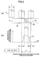
- Fig. 2 is a schematic view useful in explaining the principles on the basis of which a width of a pattern or the like is measured on the basis of the secondary electrons and the like emitted from the sample 6.
- the description will hereinbelow be given with respect to an example in which the width of a sample made of a material C and a material Ru is measured.
- the electron beam 2 has a beam diameter d, and the sample 6 is scanned with the electron beam from the left-hand side to the right-hand side in a part (a) of Fig. 2.
- a quantity of generated secondary electrons is less.
- the beam intensity shows about zero.
- the electron beam 2 comes near to a material Ru part 6b, a large number of secondary electrons begin to be emitted from the material Ru having a higher efficiency of generation of secondary electrons.
- the intensity is displayed in the form of a beam profile 12. That is to say, the beam intensity for the material Ru part 6b starts to be displayed on the image display monitor from the boundary between the material C part 6a and the material Ru part 6b by a distance corresponding to one half the electron beam diameter d, and similarly, after the scanning with the electron beam has passed the material Ru part 6b made of the material Ru, the beam intensity is displayed so widely by one half the electron beam diameter d.
- the width of the material Ru part 6b is, as a result, measured in a larger size than that of the actual dimension.
- the material Ru part 6b having an actual dimension L is measured as having the dimension Ls of the beam profile which is larger than the actual diameter L by the electron beam diameter d. Then, the diameter different from the actual diameter is measured.
- the proper measured value is obtained by subtracting the electron beam diameter d from the dimension Ls of the beam profile. According to this method, it is possible to suppress or eliminate the measurement error due to the influence of the dimension of the beam diameter.
- the evaluation of the dimension of the beam diameter is carried out using a sample for evaluation used to evaluate the dimension of the beam diameter d whenever changing the optical conditions, whenever exchanging a semiconductor wafer as an object to be measured for another one, or at arbitrary timing.
- Fig. 8A is a schematic view showing structure of an example of a sample for evaluation.
- a sample 30 for evaluation is attached to the sample holder 7, a sample stage on which the sample holder 7 is to be arranged, or an arbitrary position within a sample room self-containing a sample which is to be irradiated with the electron beam and the sample stage, and the like.
- a sequence for carrying out the evaluation of the dimension of the beam diameter at various kinds of timing as has already been described is incorporated in the system.
- Fig. 8B is a perspective view showing structure of a sample stage having a recess part 33 on which the sample 30 for evaluation is to be placed.
- the sample 30 for evaluation is made of combination of materials such as ruthenium 31 (Ru), and carbon 32 (C), or tungsten (W) and carbon (C) between the atomic numbers of which are large in difference.
- ruthenium 31 Ru
- C carbon 32
- W tungsten
- C carbon
- the sequence is incorporated therein in which when the evaluation different from that for a predetermined beam diameter is made during the evaluation of the dimension of the beam diameter, a sequence for changing predetermined optical conditions is carried out to evaluate the dimension of the beam diameter again.
- the error display may be, as a result, made or the message to urge the exchange of a sample for evaluation for another one or to urge the cleaning may be displayed on the image display monitor 10.
- the cause due to which a predetermined beam diameter can not be obtained is present in an electron microscope of the scanning electron microscope, that effect may also be displayed on the image display monitor 10.
- JP-A-11-224640 and JP-A-11-25898 may also be applied to the present invention.
- the width measurement method according to the present invention is particularly effective for a sample in which there is no difference in height between a certain device as an object to be width-measured and any of other devices, and hence no increase in a quantity of secondary electrons due to the edge effect can be expected.
- Fig. 3 is a schematic view useful in explaining the width measurement method which is adapted to measure the width between members each having a high efficiency of generation of secondary electrons. Also, Fig. 3, similarly to the example shown in Fig. 2, shows the relationship between a quantity of generated secondary electrons when scanning the member with the electron beam from the left-hand side to the right-hand side in the figure and the actual dimension.
- the actual diameter L2 can be calculated by adding the electron beam diameter d to the beam profile dimension Ln.
- the corresponding value for the beam diameter is not only added or subtracted to or from the beam profile dimension, but the arithmetic operation method and the necessity or unnecessity of the arithmetic operation should be suitably selected in correspondence to the situation of a sample.
- the value corresponding to one half the beam diameter needs to be added to the width-measured value on the side having a larger efficiency of generation of secondary electron beams, while the value corresponding to one half the beam diameter needs to be subtracted from the width-measured value on the side having a lower efficiency of generation of secondary electrons. That is to say, a quantity of correction becomes zero in total and hence the value which is obtained in the beam profile can be applied in its entirety.
- Such selection of the arithmetic operation methods and the necessity or unnecessity of the arithmetic operation is previously set on the basis of the setting by the recipe, which makes it possible to carry out the automatic inspection. That recipe is set in a recipe setting screen displayed on the image display monitor 10.
- the choices of setting an object to be width-measured there may be provided the choices of the information with respect to the arrangement of the materials adjacent to an object to be width-measured such as Rn - C - Ru or C - Ru - C.
- the correction based on the value with respect to the dimension value of the beam diameter as has already been described may also be adapted to be automatically carried out on the basis of the choices. According to the system in which such setting can be carried out, even if an operator has not especially the knowledge with respect to the present invention, he/she can automatically correct an error in width measurement on the basis of a dimension value of a beam diameter.
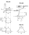
- Figs. 4A to 4C are respectively schematic views useful in explaining an example in which the dimension of a sample is measured using the applied beam with a certain beam diameter.
- the description will hereinbelow be given with respect to an example in which as shown in a part (a) of Fig. 4A, a sample 18 made of a material C part 18a and a material W part 18b is measured.
- a material W similarly to a material Ru, has a higher efficiency of generation of secondary electrons than that of a material C.
- a profile of the beam diameter as shown in a part (b) of Fig. 4A is obtained. While in the present embodiment according to the invention, a certain level of the beam profile is set as a slice level to obtain the width-measurement value on the basis of the profile of the part of interest, since the width-measured value thus obtained is different from the actual dimension, it is necessary to carry out the correction therefor.
- a profile 20 of the beam diameter when the sample 18 is irradiated with an electron beam with a beam diameter d2 is shown in a part (c) of Fig. 4A. Since the secondary electron profile changes depending on the dimension of a beam diameter, a quantity of correction becomes the function of the slice level and the beam diameter. The relationship between the slice level and the measured dimension is shown in Fig. 4B. From this figure, it is estimated that a quantity of correction is proportional to the change in slice level and the beam diameter.
- Fig. 5 is a graphical representation useful in explaining the phenomenon in which an SEM image of the width-measured value spreads depending on the dimension of the beam diameter on the basis of an actual example in which a pattern width of 0.65 ⁇ m was measured.
- an objective lens current is 1,195 mA
- the beam is condensed most slenderly to provide the width-measured value of 0.655 ⁇ m.
- the resultant width-measured value is measured so large as to be about 0.665 ⁇ m in both of the directions so that the measured pattern width becomes large depending on the dimension of the beam diameter.
- the fluctuation value of the focus may be detected to correct the dimension value of the beam diameter or the width-measured value on the basis of the fluctuation value thus detected.
- the focus When a sample, for example, is charged with electricity, the focus may be deviated due to the electrification in some cases.
- the situation of the electrification may be measured with an electrostatic measuring instrument or the like to correct the dimension value of the beam diameter or the width-measured value on the basis of the value corresponding to that situation.
- the evaluation value for a focal point is calculated in the form of a differentiated value of the intensity of the secondary electrons or the reflected electrons.
- a part in which the signal intensity changes largely in the scanning area may be judged as the position of the focal point so that the focus can not be adjusted to a bottom part or a upper surface of an irregularity in some cases. That is to say, when an object to be width-measured is a upper part of a convex pattern or the internal part of a contact hole, the width of an object to be width-measured is measured with the electron beam being out of focus.
- a quantity of correction for a beam diameter or a quantity of correction for a width-measured value is previously stored every object to be observed, and when an object to be observed of interest is selected, such a quantity of correction is added or subtracted, which makes it possible to obtain the accurate dimension value of the beam diameter or the accurate width-measured value.
- a quantity of correction to be changed is stored in the form of a correction coefficiency and a beam diameter or a width-measured value is multiplied or divided by this correction efficiency to obtain the accurate dimension value of a beam diameter or an accurate width-measured value.
- Fig. 6A is a schematic diagram useful in explaining the phenomenon in which the SEM image of the width-measured value spreads depending on the dimension of a beam diameter using a sample 22 in which the dimension of a multi-layer film is known.
- the sample 22 is a multi-layer film and is made of a material C part 22a and a material W part 22b.
- the width of the material C part 22a is 11.1 nm and the width of the material W part 22b is 5.6 nm.
- the width-measured value of the material W part 22b was, as a result, 9.4 nm and the with-measured value of the material C part 22a was 7.3 nm at the acceleration voltage of 1 kV.
- the measured width of the material W part 22b was larger than the actual dimension by 3.8 nm.
- the measured width of the material W part 22b was larger than the actual dimension by 1.8 nm.
- a displayed image corresponding to the dimension value of the measured width is larger than the actual dimension by the corresponding quantity for the beam diameter.
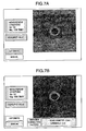
- Figs. 7A and 7B show an example of the display on the image display monitor.
- Fig. 7A shows the case where the width of an object to be width-measured is measured with an automatic mode.
- Fig. 7B shows the case where the width of an object to be width-measured is measured with a manual mode. Then, in the case of the manual mode, dimension correction factors and their values are adapted to be displayed and hence the grounds of the dimension correction are clearly demonstrated.
- the present embodiment when a pattern having a pitch of 30 nm, for example, is measured with a beam with a diameter of 3 nm, though the pattern is formed at pitch of 30 nm, and at pitch of 30 nm in real dimension, the measured dimension of the pattern are respectively at pitch of 33 nm and at pitch of 27 nm in accordance with the conventional method, the difference from other systems (TEM (Transmission Electron Microscope) and the like) becomes a problem.
- TEM Transmission Electron Microscope
- the measurement result is corrected with a correction value from the beam profile which is previously measured, whereby it is possible to solve the present problem.
- a scanning electron microscope for measuring the dimension of a pattern on a semiconductor wafer is adapted to measure a plurality of places to be width-measured on the same semiconductor wafer. Then, if the dimension of an electron beam diameter is measured at timing which does not permit predetermined throughput to be reduced in terms of a semiconductor inspection system, and the resultant dimension of the beam diameter is corrected every width-measured place in accordance with the situation of charge-up of a semiconductor wafer, the kind of object to be width-measured and the like to be used, then it is possible to carry out the width measurement of a pattern with high accuracy while maintaining the throughput.
- the present invention is not intended to be limited thereto. That is to say, the present invention may also be applied to all of systems for detecting a secondary signal (secondary electrons, reflected electrons, light, X-rays or the like) obtained by scanning a sample with a beam to measure the dimension of a pattern on the sample.
- a scanning ion microscope for scanning a sample with an ion beam to detect the resultant secondary electrons or secondary ions
- a laser microscope using a laser beam an X-ray microscope for applying X-rays, and the like.
- the error resulting from the diameter of the beam is reduced or eliminated in the present method by correcting the measured value with a value relating to the beam diameter.
Landscapes
- Chemical & Material Sciences (AREA)
- Analytical Chemistry (AREA)
- Physics & Mathematics (AREA)
- Electromagnetism (AREA)
- General Physics & Mathematics (AREA)
- Length-Measuring Devices Using Wave Or Particle Radiation (AREA)
- Testing Or Measuring Of Semiconductors Or The Like (AREA)
Abstract
Description
Claims (7)
- A width-measurement method of scanning a sample (6, 14, 18, 22, 30) with a beam (2) to measure a width of an object (6b, 14a, 18b, 22a, 22b) to be width-measured on said sample on the basis of a secondary signal obtained from said sample,
wherein a width-measured value of said object to be width-measured which has been obtained on the basis of the secondary signal is corrected with a dimension value of the beam diameter (d). - A width-measurement method of scanning a sample (6, 14, 18, 22, 30) with a beam (2) to measure a width of an object (6b, 14a, 18b, 22a, 22b) to be width-measured on said sample on the basis of a secondary signal obtained from said sample,
wherein the dimension of a beam diameter (d) of said beam is previously measured; a beam profile (12, 16, 19, 20) of said beam is formed on the basis of the secondary signal which has been obtained from said sample by scanning said sample with said beam; the width-measurement of said object to be width-measured is made on the basis of said beam profile; and a value with respect to the dimension value of the beam diameter, or a value which is obtained by correcting the value with respect to the dimension value of the beam diameter is either added or subtracted to or from the width-measured value of said object to be width-measured. - A width-measurement method according to claim 2, wherein the dimension of the beam diameter is corrected in accordance with the degree of focus of the beam.
- A width-measurement method according to claim 2, wherein when a width of a sample part (6b, 18b, 22b) having a higher efficiency of generation of a secondary signal is measured with respect to parts adjacent to each other, the value with respect to the dimension of the beam diameter is subtracted from the width-measured value, while when a width of a sample part (14a, 22a) having a lower efficiency of generation of a secondary signal is measured with respect to parts adjacent to each other, the value with respect to the dimension of the beam diameter is added to the width-measured value.
- A scanning electron microscope for scanning a sample (6, 14, 22, 30) with a beam (2) to measure a width of an object (6b, 14a, 18b, 22a, 22b) to be width-measured on said sample on the basis of a secondary signal obtained from said sample,
wherein a width-measured value of said object to be width-measured which has been obtained on the basis of the secondary signal is corrected with a value with respect to the dimension value of the beam diameter. - A scanning charged particle microscope including: a charged particle gun (1); a lens (3) for condensing a charged particle beam (2) drawn from said charged particle gun; a deflecting system (4) for scanning a sample (6, 14, 18, 22, 30) with the charged particle beam; a detector (8) for detecting a secondary signal emitted from said sample by irradiating said sample with the charged particle beam; and a function of measuring a width of an object (6b, 14a, 18b, 22a, 22b) to be width-measured on said sample on the basis of the secondary signal detected by said detector, said microscope comprising:means (9, 10) for forming a beam profile (12, 16, 19, 20) on the basis of the secondary signal detected by said detector;means (9, 10) for measuring the dimension of said object to be width-measured on the basis of the beam profile; andmeans (9, 10) for correcting the dimension-measured value obtained by said measurement means with a value with respect to the dimension value of the charged particle beam diameter (d).
- A scanning charged particle microscope according to claim 9, wherein a sample room in which a sample to be irradiated with the charged particle beam is to be arranged is provided with a sample for evaluation used to evaluate the diameter of the charged particle beam.
Applications Claiming Priority (2)
| Application Number | Priority Date | Filing Date | Title |
|---|---|---|---|
| JP2001314695A JP3944373B2 (en) | 2001-10-12 | 2001-10-12 | Sample length measuring method and scanning microscope |
| JP2001314695 | 2001-10-12 |
Publications (2)
| Publication Number | Publication Date |
|---|---|
| EP1302972A2 true EP1302972A2 (en) | 2003-04-16 |
| EP1302972A3 EP1302972A3 (en) | 2005-02-02 |
Family
ID=19132961
Family Applications (1)
| Application Number | Title | Priority Date | Filing Date |
|---|---|---|---|
| EP02021294A Withdrawn EP1302972A3 (en) | 2001-10-12 | 2002-09-19 | Method and scanning electron microscope for measuring width of material on sample |
Country Status (4)
| Country | Link |
|---|---|
| US (2) | US6791084B2 (en) |
| EP (1) | EP1302972A3 (en) |
| JP (1) | JP3944373B2 (en) |
| KR (1) | KR100893910B1 (en) |
Families Citing this family (36)
| Publication number | Priority date | Publication date | Assignee | Title |
|---|---|---|---|---|
| US20070228287A1 (en) * | 2006-03-20 | 2007-10-04 | Alis Technology Corporation | Systems and methods for a gas field ionization source |
| US7786452B2 (en) | 2003-10-16 | 2010-08-31 | Alis Corporation | Ion sources, systems and methods |
| US7557360B2 (en) * | 2003-10-16 | 2009-07-07 | Alis Corporation | Ion sources, systems and methods |
| US7368727B2 (en) * | 2003-10-16 | 2008-05-06 | Alis Technology Corporation | Atomic level ion source and method of manufacture and operation |
| US7786451B2 (en) * | 2003-10-16 | 2010-08-31 | Alis Corporation | Ion sources, systems and methods |
| US7554096B2 (en) * | 2003-10-16 | 2009-06-30 | Alis Corporation | Ion sources, systems and methods |
| US7557361B2 (en) * | 2003-10-16 | 2009-07-07 | Alis Corporation | Ion sources, systems and methods |
| US7601953B2 (en) * | 2006-03-20 | 2009-10-13 | Alis Corporation | Systems and methods for a gas field ion microscope |
| US7554097B2 (en) * | 2003-10-16 | 2009-06-30 | Alis Corporation | Ion sources, systems and methods |
| US7521693B2 (en) * | 2003-10-16 | 2009-04-21 | Alis Corporation | Ion sources, systems and methods |
| US7495232B2 (en) * | 2003-10-16 | 2009-02-24 | Alis Corporation | Ion sources, systems and methods |
| US7504639B2 (en) * | 2003-10-16 | 2009-03-17 | Alis Corporation | Ion sources, systems and methods |
| US7485873B2 (en) * | 2003-10-16 | 2009-02-03 | Alis Corporation | Ion sources, systems and methods |
| US8110814B2 (en) | 2003-10-16 | 2012-02-07 | Alis Corporation | Ion sources, systems and methods |
| US7518122B2 (en) | 2003-10-16 | 2009-04-14 | Alis Corporation | Ion sources, systems and methods |
| US7557359B2 (en) * | 2003-10-16 | 2009-07-07 | Alis Corporation | Ion sources, systems and methods |
| US7557358B2 (en) | 2003-10-16 | 2009-07-07 | Alis Corporation | Ion sources, systems and methods |
| US7511279B2 (en) * | 2003-10-16 | 2009-03-31 | Alis Corporation | Ion sources, systems and methods |
| US7488952B2 (en) * | 2003-10-16 | 2009-02-10 | Alis Corporation | Ion sources, systems and methods |
| US7511280B2 (en) * | 2003-10-16 | 2009-03-31 | Alis Corporation | Ion sources, systems and methods |
| US7321118B2 (en) * | 2005-06-07 | 2008-01-22 | Alis Corporation | Scanning transmission ion microscope |
| US9159527B2 (en) | 2003-10-16 | 2015-10-13 | Carl Zeiss Microscopy, Llc | Systems and methods for a gas field ionization source |
| US7414243B2 (en) * | 2005-06-07 | 2008-08-19 | Alis Corporation | Transmission ion microscope |
| JP4500099B2 (en) * | 2004-05-06 | 2010-07-14 | 株式会社日立ハイテクノロジーズ | Electron microscope apparatus system and dimension measuring method using electron microscope apparatus system |
| JP4338627B2 (en) * | 2004-12-17 | 2009-10-07 | 株式会社日立ハイテクノロジーズ | Charged particle beam apparatus and charged particle beam microscopic method |
| JP4719554B2 (en) * | 2005-11-10 | 2011-07-06 | 株式会社日立ハイテクノロジーズ | Focused ion beam device |
| US20070116373A1 (en) * | 2005-11-23 | 2007-05-24 | Sonosite, Inc. | Multi-resolution adaptive filtering |
| JP5099291B2 (en) * | 2006-02-14 | 2012-12-19 | エスアイアイ・ナノテクノロジー株式会社 | Focused ion beam apparatus and sample cross-section processing and observation method |
| WO2007109666A2 (en) * | 2006-03-20 | 2007-09-27 | Alis Corporation | Systems and methods for a helium ion pump |
| KR100822791B1 (en) * | 2006-07-28 | 2008-04-17 | 장동영 | Compact Electronic Scanning Microscope |
| US7804068B2 (en) | 2006-11-15 | 2010-09-28 | Alis Corporation | Determining dopant information |
| US7791022B2 (en) * | 2007-03-13 | 2010-09-07 | Advantest Corp. | Scanning electron microscope with length measurement function and dimension length measurement method |
| JP4764436B2 (en) * | 2008-02-14 | 2011-09-07 | 株式会社日立ハイテクノロジーズ | Appearance inspection method and inspection apparatus |
| DE112008004172T5 (en) | 2008-12-26 | 2012-03-15 | Advantest Corporation | Structural measuring device and structural measuring method |
| JP4929296B2 (en) | 2009-01-28 | 2012-05-09 | 株式会社日立ハイテクノロジーズ | Charged particle beam equipment |
| EP3571531A4 (en) * | 2017-01-23 | 2020-08-05 | Shenzhen Xpectvision Technology Co., Ltd. | X-RAY DETECTORS WITH THE ABILITY TO IDENTIFY AND MANAGE CHARGE SHARING |
Citations (1)
| Publication number | Priority date | Publication date | Assignee | Title |
|---|---|---|---|---|
| EP0877409A2 (en) * | 1997-05-08 | 1998-11-11 | Hitachi, Ltd. | Resolving power evaluation method and specimen for electron microscope |
Family Cites Families (7)
| Publication number | Priority date | Publication date | Assignee | Title |
|---|---|---|---|---|
| JPS6342407A (en) | 1986-08-07 | 1988-02-23 | Matsushita Electric Ind Co Ltd | Measuring method for pattern line width |
| JPH0690017B2 (en) | 1989-01-20 | 1994-11-14 | 日本電子株式会社 | Charged particle beam length measurement method |
| JP2647732B2 (en) * | 1990-06-27 | 1997-08-27 | 株式会社日立製作所 | Electron beam size measurement device |
| JPH06347246A (en) | 1993-06-07 | 1994-12-20 | Hitachi Ltd | Scanning electron microscope with length measurement function |
| JPH09184714A (en) * | 1995-12-28 | 1997-07-15 | Hitachi Ltd | Pattern dimension measurement method |
| JPH11224640A (en) | 1998-02-10 | 1999-08-17 | Hitachi Ltd | Electron microscope, resolution evaluation method thereof, and semiconductor manufacturing method using the same |
| US6396059B1 (en) * | 2000-07-10 | 2002-05-28 | Advanced Micro Devices, Inc. | Using a crystallographic etched silicon sample to measure and control the electron beam width of a SEM |
-
2001
- 2001-10-12 JP JP2001314695A patent/JP3944373B2/en not_active Expired - Fee Related
-
2002
- 2002-09-19 EP EP02021294A patent/EP1302972A3/en not_active Withdrawn
- 2002-09-19 US US10/246,453 patent/US6791084B2/en not_active Expired - Lifetime
- 2002-10-11 KR KR1020020062036A patent/KR100893910B1/en not_active Expired - Fee Related
-
2004
- 2004-08-05 US US10/911,480 patent/US7385196B2/en not_active Expired - Fee Related
Patent Citations (1)
| Publication number | Priority date | Publication date | Assignee | Title |
|---|---|---|---|---|
| EP0877409A2 (en) * | 1997-05-08 | 1998-11-11 | Hitachi, Ltd. | Resolving power evaluation method and specimen for electron microscope |
Also Published As
| Publication number | Publication date |
|---|---|
| US7385196B2 (en) | 2008-06-10 |
| US20030071214A1 (en) | 2003-04-17 |
| JP3944373B2 (en) | 2007-07-11 |
| US20050006581A1 (en) | 2005-01-13 |
| KR100893910B1 (en) | 2009-04-21 |
| JP2003121132A (en) | 2003-04-23 |
| US6791084B2 (en) | 2004-09-14 |
| KR20030030972A (en) | 2003-04-18 |
| EP1302972A3 (en) | 2005-02-02 |
Similar Documents
| Publication | Publication Date | Title |
|---|---|---|
| US6791084B2 (en) | Method and scanning electron microscope for measuring dimension of material on sample | |
| KR101438068B1 (en) | High electron energy based overlay error measurement methods and systems | |
| US8487250B2 (en) | Method for detecting information of an electronic potential on a sample and charged particle beam apparatus | |
| US6265719B1 (en) | Inspection method and apparatus using electron beam | |
| US8080789B2 (en) | Sample dimension measuring method and scanning electron microscope | |
| JP5357889B2 (en) | Charged particle beam equipment | |
| EP1238405B1 (en) | Method and system for the examination of specimen using a charged particle beam | |
| US8080790B2 (en) | Scanning electron microscope | |
| US20080017797A1 (en) | Pattern inspection and measurement apparatus | |
| WO2011013342A1 (en) | Pattern evaluation method, device therefor, and electron beam device | |
| US7521678B2 (en) | Charged particle beam apparatus, charged particle beam focusing method, microstructure measuring method, microstructure inspecting method, semiconductor device manufacturing method, and program | |
| JP2000123768A (en) | Charged particle beam apparatus, method of adjusting charged particle beam apparatus, and method of manufacturing semiconductor device | |
| JP2007187538A (en) | Charged particle beam apparatus and image acquisition method using the same | |
| JP2001052642A (en) | Scanning electron microscope and fine pattern measurement method | |
| JP3836735B2 (en) | Circuit pattern inspection device | |
| JP4298938B2 (en) | Charged particle beam equipment | |
| JP2008084823A (en) | Charged particle beam adjustment method and charged particle beam apparatus | |
| JP4141785B2 (en) | Pattern width measuring apparatus, pattern width measuring method, and electron beam exposure apparatus | |
| JP2000077019A (en) | electronic microscope | |
| JPH10269982A (en) | Lens voltage setting method of inspection device and inspection device | |
| TW202042272A (en) | Method for determining observation conditions in charged particle beam system and charged particle beam device | |
| JP5470360B2 (en) | Sample potential information detection method and charged particle beam apparatus | |
| JP5174483B2 (en) | Charged particle beam apparatus and method for knowing charged state of sample surface | |
| JP2013178877A (en) | Charged particle beam device | |
| JP2009016361A (en) | Charged particle beam equipment |
Legal Events
| Date | Code | Title | Description |
|---|---|---|---|
| PUAI | Public reference made under article 153(3) epc to a published international application that has entered the european phase |
Free format text: ORIGINAL CODE: 0009012 |
|
| AK | Designated contracting states |
Designated state(s): AT BE BG CH CY CZ DE DK EE ES FI FR GB GR IE IT LI LU MC NL PT SE SK TR |
|
| AX | Request for extension of the european patent |
Extension state: AL LT LV MK RO SI |
|
| PUAL | Search report despatched |
Free format text: ORIGINAL CODE: 0009013 |
|
| AK | Designated contracting states |
Kind code of ref document: A3 Designated state(s): AT BE BG CH CY CZ DE DK EE ES FI FR GB GR IE IT LI LU MC NL PT SE SK TR |
|
| AX | Request for extension of the european patent |
Extension state: AL LT LV MK RO SI |
|
| 17P | Request for examination filed |
Effective date: 20050217 |
|
| 17Q | First examination report despatched |
Effective date: 20050609 |
|
| AKX | Designation fees paid |
Designated state(s): DE FR GB |
|
| GRAP | Despatch of communication of intention to grant a patent |
Free format text: ORIGINAL CODE: EPIDOSNIGR1 |
|
| INTG | Intention to grant announced |
Effective date: 20160413 |
|
| STAA | Information on the status of an ep patent application or granted ep patent |
Free format text: STATUS: THE APPLICATION IS DEEMED TO BE WITHDRAWN |
|
| 18D | Application deemed to be withdrawn |
Effective date: 20160824 |