EP1302787A2 - Optical sheet and display device having the optical sheet - Google Patents
Optical sheet and display device having the optical sheet Download PDFInfo
- Publication number
- EP1302787A2 EP1302787A2 EP02022929A EP02022929A EP1302787A2 EP 1302787 A2 EP1302787 A2 EP 1302787A2 EP 02022929 A EP02022929 A EP 02022929A EP 02022929 A EP02022929 A EP 02022929A EP 1302787 A2 EP1302787 A2 EP 1302787A2
- Authority
- EP
- European Patent Office
- Prior art keywords
- transparent
- light
- fine
- optical sheet
- diffusing layer
- Prior art date
- Legal status (The legal status is an assumption and is not a legal conclusion. Google has not performed a legal analysis and makes no representation as to the accuracy of the status listed.)
- Ceased
Links
Images








Classifications
-
- G—PHYSICS
- G02—OPTICS
- G02F—OPTICAL DEVICES OR ARRANGEMENTS FOR THE CONTROL OF LIGHT BY MODIFICATION OF THE OPTICAL PROPERTIES OF THE MEDIA OF THE ELEMENTS INVOLVED THEREIN; NON-LINEAR OPTICS; FREQUENCY-CHANGING OF LIGHT; OPTICAL LOGIC ELEMENTS; OPTICAL ANALOGUE/DIGITAL CONVERTERS
- G02F1/00—Devices or arrangements for the control of the intensity, colour, phase, polarisation or direction of light arriving from an independent light source, e.g. switching, gating or modulating; Non-linear optics
- G02F1/01—Devices or arrangements for the control of the intensity, colour, phase, polarisation or direction of light arriving from an independent light source, e.g. switching, gating or modulating; Non-linear optics for the control of the intensity, phase, polarisation or colour
- G02F1/13—Devices or arrangements for the control of the intensity, colour, phase, polarisation or direction of light arriving from an independent light source, e.g. switching, gating or modulating; Non-linear optics for the control of the intensity, phase, polarisation or colour based on liquid crystals, e.g. single liquid crystal display cells
- G02F1/133—Constructional arrangements; Operation of liquid crystal cells; Circuit arrangements
- G02F1/1333—Constructional arrangements; Manufacturing methods
- G02F1/1335—Structural association of cells with optical devices, e.g. polarisers or reflectors
-
- G—PHYSICS
- G03—PHOTOGRAPHY; CINEMATOGRAPHY; ANALOGOUS TECHNIQUES USING WAVES OTHER THAN OPTICAL WAVES; ELECTROGRAPHY; HOLOGRAPHY
- G03B—APPARATUS OR ARRANGEMENTS FOR TAKING PHOTOGRAPHS OR FOR PROJECTING OR VIEWING THEM; APPARATUS OR ARRANGEMENTS EMPLOYING ANALOGOUS TECHNIQUES USING WAVES OTHER THAN OPTICAL WAVES; ACCESSORIES THEREFOR
- G03B21/00—Projectors or projection-type viewers; Accessories therefor
- G03B21/54—Accessories
- G03B21/56—Projection screens
-
- G—PHYSICS
- G02—OPTICS
- G02B—OPTICAL ELEMENTS, SYSTEMS OR APPARATUS
- G02B3/00—Simple or compound lenses
- G02B3/0006—Arrays
- G02B3/0012—Arrays characterised by the manufacturing method
- G02B3/0031—Replication or moulding, e.g. hot embossing, UV-casting, injection moulding
-
- G—PHYSICS
- G02—OPTICS
- G02B—OPTICAL ELEMENTS, SYSTEMS OR APPARATUS
- G02B3/00—Simple or compound lenses
- G02B3/0006—Arrays
- G02B3/0037—Arrays characterized by the distribution or form of lenses
- G02B3/0056—Arrays characterized by the distribution or form of lenses arranged along two different directions in a plane, e.g. honeycomb arrangement of lenses
-
- G—PHYSICS
- G02—OPTICS
- G02B—OPTICAL ELEMENTS, SYSTEMS OR APPARATUS
- G02B5/00—Optical elements other than lenses
- G02B5/02—Diffusing elements; Afocal elements
- G02B5/0205—Diffusing elements; Afocal elements characterised by the diffusing properties
- G02B5/0236—Diffusing elements; Afocal elements characterised by the diffusing properties the diffusion taking place within the volume of the element
- G02B5/0242—Diffusing elements; Afocal elements characterised by the diffusing properties the diffusion taking place within the volume of the element by means of dispersed particles
-
- G—PHYSICS
- G02—OPTICS
- G02B—OPTICAL ELEMENTS, SYSTEMS OR APPARATUS
- G02B5/00—Optical elements other than lenses
- G02B5/02—Diffusing elements; Afocal elements
- G02B5/0273—Diffusing elements; Afocal elements characterized by the use
- G02B5/0278—Diffusing elements; Afocal elements characterized by the use used in transmission
-
- G—PHYSICS
- G02—OPTICS
- G02F—OPTICAL DEVICES OR ARRANGEMENTS FOR THE CONTROL OF LIGHT BY MODIFICATION OF THE OPTICAL PROPERTIES OF THE MEDIA OF THE ELEMENTS INVOLVED THEREIN; NON-LINEAR OPTICS; FREQUENCY-CHANGING OF LIGHT; OPTICAL LOGIC ELEMENTS; OPTICAL ANALOGUE/DIGITAL CONVERTERS
- G02F1/00—Devices or arrangements for the control of the intensity, colour, phase, polarisation or direction of light arriving from an independent light source, e.g. switching, gating or modulating; Non-linear optics
- G02F1/01—Devices or arrangements for the control of the intensity, colour, phase, polarisation or direction of light arriving from an independent light source, e.g. switching, gating or modulating; Non-linear optics for the control of the intensity, phase, polarisation or colour
- G02F1/13—Devices or arrangements for the control of the intensity, colour, phase, polarisation or direction of light arriving from an independent light source, e.g. switching, gating or modulating; Non-linear optics for the control of the intensity, phase, polarisation or colour based on liquid crystals, e.g. single liquid crystal display cells
- G02F1/133—Constructional arrangements; Operation of liquid crystal cells; Circuit arrangements
- G02F1/1333—Constructional arrangements; Manufacturing methods
- G02F1/1335—Structural association of cells with optical devices, e.g. polarisers or reflectors
- G02F1/133504—Diffusing, scattering, diffracting elements
-
- G—PHYSICS
- G02—OPTICS
- G02F—OPTICAL DEVICES OR ARRANGEMENTS FOR THE CONTROL OF LIGHT BY MODIFICATION OF THE OPTICAL PROPERTIES OF THE MEDIA OF THE ELEMENTS INVOLVED THEREIN; NON-LINEAR OPTICS; FREQUENCY-CHANGING OF LIGHT; OPTICAL LOGIC ELEMENTS; OPTICAL ANALOGUE/DIGITAL CONVERTERS
- G02F1/00—Devices or arrangements for the control of the intensity, colour, phase, polarisation or direction of light arriving from an independent light source, e.g. switching, gating or modulating; Non-linear optics
- G02F1/01—Devices or arrangements for the control of the intensity, colour, phase, polarisation or direction of light arriving from an independent light source, e.g. switching, gating or modulating; Non-linear optics for the control of the intensity, phase, polarisation or colour
- G02F1/13—Devices or arrangements for the control of the intensity, colour, phase, polarisation or direction of light arriving from an independent light source, e.g. switching, gating or modulating; Non-linear optics for the control of the intensity, phase, polarisation or colour based on liquid crystals, e.g. single liquid crystal display cells
- G02F1/133—Constructional arrangements; Operation of liquid crystal cells; Circuit arrangements
- G02F1/1333—Constructional arrangements; Manufacturing methods
- G02F1/1335—Structural association of cells with optical devices, e.g. polarisers or reflectors
- G02F1/133526—Lenses, e.g. microlenses or Fresnel lenses
-
- G—PHYSICS
- G02—OPTICS
- G02B—OPTICAL ELEMENTS, SYSTEMS OR APPARATUS
- G02B3/00—Simple or compound lenses
- G02B3/0006—Arrays
- G02B3/0037—Arrays characterized by the distribution or form of lenses
- G02B3/005—Arrays characterized by the distribution or form of lenses arranged along a single direction only, e.g. lenticular sheets
Definitions
- the present invention relates to an optical sheet used as a transmission type screen member in a back projection type display device or as a viewing angle enlarging member in a liquid-crystal display device, and a display device using the optical sheet.
- a back projection type display device using a liquid-crystal display element or a dot matrix display element such as a digital mirror device has a projector for outputting image light formed through a display element, a reflectingmirror having a function of reflecting the image light outputted from the projector to change the direction of movement of the image light, and a transmission type screen for spreading the incident image light moderately to the observer side to display an image.
- the transmission type screen includes a Fresnel lens sheet, and a lenticular lens sheet.
- the Fresnel lens sheet is an optical component having the same function as that of a convex lens. That is, the Fresnel lens sheet has a function of changing the direction of the image light outputted from the projector to the observer side to enlarge an optimal viewing range.
- the lenticular lens sheet has a function of distributing the limited image light outputted from the projector into an observer's observation range effectively.
- the lenticular lens sheet includes a plurality of cylindrical lenses arrayed in one direction, and a light absorbing layer disposed in other regions than light-condensing regions through the lenses for absorbing light inputted from the environment surrounding the lenticular lens sheet (hereinafter, the light being referred to as "external light”) .
- the light being referred to as "external light”
- focal points of the lenses are located on an observation surface of the screen, reflection of the external light is reduced without any loss of the image light ideally to thereby suppress lowering of contrast ratio under the bright environment.
- Unexamined Japanese Patent Publication No. Hei. 10-260638 has disclosed a lenticular lens sheet having a transparent resin formed as lenses for achieving a wide viewing angle and a bright image, a light absorbing layer patterned, and a diffusing layer having a thickness of from 20 to 500 ⁇ m and laminated between the transparent resin and the light absorbing layer.
- a direct-vision liquid-crystal display device using TN (Twisted Nematic) liquid crystal or the like generally has viewing angle dependence in which luminance or chromaticity varies in accordance with the direction of observation.
- Unexamined Japanese Patent Publication No. Hei. 10-39769 has described an optical member which can eliminate the view angle dependence and reduce reflection of external light to thereby suppress lowering of contrast ratio under the bright environment when the optical member is disposed in front of a liquid-crystal display device.
- the optical member is provided as a micro lens array sheet having a transparent substrate, a plurality of micro lenses constituted by fine convex surfaces and arrayed planarly on one surface of the transparent substrate, and a light absorbing layer disposed on the other surface of the transparent substrate and having opening portions located in places corresponding to apices of convex portions of the micro lenses.
- Examples of the method for producing lenses of an optical member such as a lenticular lens sheet or a micro lens array sheet applied to a display device include: a method using a mold such as a metal mold, a resin mold or a stamper for transferring the shape of the mold; and a method of forming patterns from a resist material at intervals of a required pitch by photolithography and hot-melting the patterns.
- a method using a metal mold for transferring the shape of the mold is most preferred as the method for producing a large-area lens array inexpensively.
- a transparent resin such as an ultraviolet-setting resin, a thermosetting resin or a thermoplastic resin is used as the lens material.
- the refractive index of the practical lens material is in a range of from about 1.48 to about 1.66.
- Fig. 21 is a graph showing the relation between luminance and viewing angle characteristic in accordance with the refractive index n of a lens.
- Fig. 21 shows results of calculation in the case where rays of parallel light are incident on a hemispherical lens.
- the horizontal axis shows an emission angle (viewing angle)
- the vertical axis shows a relative value of luminance.
- the difference between luminance in a frontal direction (at an emission angle of 0 degrees) and luminance in an oblique direction decreases so that the viewing angle is widened.
- TCO 99 cannot be satisfied even in the case where the refractive index of a lens is 1.7, in accordance with the estimation. That is, an optical member capable of achieving a sufficient viewing angle cannot be obtained by use of only the refracting function of a lens using a practical lens material. It is therefore necessary to provide a diffusing layer for enlarging the viewing angle.
- a lenticular lens sheet having a transparent substrate including lenses formed on one surface, a light absorbing layer, and a diffusing layer laminated between the transparent substrate and the light absorbing layer.
- the thickness of the diffusing layer is defined to be in a range of from 20 to 500 ⁇ m from the point of view of preventing generation of a hot band and suppressing lowering of light transmittance but there is no particular consideration for display of a high-precision image.
- the resolution of an image displayed on a general optical sheet such as a lenticular lens sheet or a micro lens array sheet depends on the pitch of lenses arrayed. As the pitch of lenses decreases, a higher-precision image can be displayed. It is therefore necessary that the pitch of lenses constituting an optical member is selected to be not larger than tens of microns in order to meet higher resolution of an image advanced with the popularization of HDTV (High Definition Television) in the future.
- HDTV High Definition Television
- Fig. 22 is a partly schematic sectional view of an optical sheet for explaining a problem in the case where the thickness d of the diffusing layer is not sufficiently small compared with the lens pitch.
- Image light 2101 incident on an optical sheet is refracted by lenses 2000 so as to be condensed into a diffusing layer 2001. If the diffusing layer is not sufficiently thin, a part 2100 of light scattered by the diffusing layer is absorbed to a light absorbing layer 2002 to thereby cause a problem that transmittance is reduced.
- opening portions 2003 of the light absorbing layer are widened in order to suppress the reduction of transmittance.
- opening portions 2003 of the light absorbing layer are widened in order to suppress the reduction of transmittance.
- the diffusing characteristic of the diffusing layer is reduced in order to suppress the reduction of transmittance. In this case, however, there arises a problem that the viewing angle is narrowed.
- the thickness of the diffusing layer is selected to be not smaller than 20 ⁇ m in the condition that the pitch of lenses is selected to be 50 ⁇ m in order to satisfy high-precision image display, there arises a problem that transmittance is reduced or contrast ratio is lowered.
- an object of the invention is to provide an optical sheet which can exhibit high transmittance and have a viewing angle even in the case where the pitch of lenses is not larger than tens of microns in order to support high-precision image display and which can achieve high-contrast-ratio display even under the bright environment; and to provide a display device using the optical sheet.
- an optical sheet has: a transparent base material; a fine lens array constituted by a plurality of fine unit lenses formed on a front surface of the transparent base material; a diffusing layer formed on a rear surface of the transparent base material opposite to the surface on which the fine lens array is formed; and a light absorbing layer formed on the diffusing layer and including fine opening portions substantially located at focal points of the unit lenses; wherein: the diffusing layer is made of a transparent medium containing transparent fine particles different in refractive index from the transparent medium; and the transparent fine particles have a mean particle size in a particle size range for maximizing a value of Q/R at each of wavelengths in a visible region when Q is a scattering sectional area per transparent fine particle, and R is a radius of each of the transparent fine particles.
- the transparent fine particles contained in the diffusing layer have a mean particle size in a particle size range for maximizing the value of Q/R at each of wavelengths in a visible region, or in a range which is near the particle size range and in which variation in the value of Q/R due to the wavelengths in the visible region is reduced.
- the diffusing layer As the value of Q/R increases, the light scattering characteristic of the diffusing layer increases exponentially. Hence, when the diffusing layer is formed in these conditions, required light scattering characteristic can be achieved though the diffusing layer is thinner.
- the value of Q/R with respect to particle sizes of the transparent fine particles varies in accordance with wavelengths.
- the mean particle size of the transparent fine particles is selected from a particle size range for maximizing the value of Q/R at wavelengths in a visible region, required light scattering characteristic can be achieved though the diffusing layer is thinner.
- transparent fine particles are used to have a mean particle size set as a particle size for maximizing the value of Q/R in a wavelength range of from 525 to 575 nm high in relative luminous efficiency, preferably at a wavelength of 550 nm, required scattering characteristic can be achieved by the diffusing layer smaller in thickness because light scattering characteristic actually sensed by the human being increases apparently.
- Variation in the value of Q/R in accordance with wavelengths means variation in scattering characteristic in accordance with colors. That is, if a particle size in which the value of Q/R varies widely in accordance with wavelengths is used, there is the possibility that image quality may deteriorate because of variation in color in accordance with the angle of observation.
- the mean particle size of the transparent fine particles is selected to be in a particle size range for maximizing the value of Q/R or in a range which is near the particle size range and in which variation in the value of Q/R in accordance with wavelengths in a visible region is reduced, variation in color in accordance with the angle of observation can be suppressed.
- the diffusing layer When the diffusing layer is thin, there can be achieved an optical sheet which is high in transmittance, small in size of the opening portions of the light absorbing layer and small in reflection of external light even in the case where the pitch of lenses in the fine lens array is reduced in order to satisfy high-precision image display.
- the bottom surface of each of the unit lenses constituting the fine lens array is basically shaped like a hexagon so that the unit lenses are arranged so as to be closest packed. Hence, the area occupied by the unit lenses in the surface of formation of the fine lens array can be increased to thereby achieve higher transmittance.
- interior angles of the shape of the bottom surface of each of the unit lenses are all selected to be not lower than 90 degrees, preferably not lower than 100 degrees. Hence, the curvature of lens surfaces in corners of each unit lens and in regions near the corners is prevented from varying widely. Accordingly, the region effectively functioning as a lens can be widened to the utmost to thereby improve transmittance more greatly.
- the longitudinal length of the shape of the bottom surface in each of the unit lenses is selected to be larger than the transverse length thereof.
- a high-contrast-ratio high-quality image can be obtained with high precision and high luminance at a wide viewing angle because of achievement of low-luminance black display even under the bright environment.
- the optical sheet according to the invention is disposed on the front surface of a direct-vision liquid-crystal display element while a backlight unit for outputting substantially parallel light rays is disposed on the rear surface side of the direct-vision liquid-crystal display element, only light in a limited range near the front of the liquid-crystal display element and permitting good image quality to be obtained can be spread isotropically by the optical sheet.
- a liquid-crystal display device for displaying a high-contrast-ratio image in a wide viewing angle range without variation in color tone and without inversion in gradation.
- Figs. 1 and 2 are a partly perspective view and a partly sectional view showing an example of an optical sheet according to the invention.
- the optical sheet 30 has a planar transparent base material 200, a micro lens array 100 formed on a front surface of the transparent base material 200, a diffusing layer 500 formed on a rear surface of the transparent base material 200, and a light absorbing layer 300 laminated to the diffusing layer 500.
- the light absorbing layer 300 has opening portions 400 located in positions corresponding to apices of convex portions of the micro lens array 100.
- the transparent base material 200 is not particularly limited if it is a material transmitting at least visible light.
- glass or any kind of plastics can be used as the transparent base material 200.
- a plastic material is preferred from the point of view of mechanical strength, reduction in thickness and weight, processability, etc.
- the plastic material may include acrylic-based resin, polycarbonate, polyethylene terephthalate, and triacetyl cellulose.
- the micro lens array 100 is constituted by fine convex portions (hereinafter referred to as "unit lenses 110") having lens functions and arranged cyclically on the transparent base material 200.
- the micro lens array 100 include: a so-called one-dimensional lens array having unit lenses each of which is constituted by a curved surface expressed in a locus of parallel translation of a curve such as a circular arc as used in a lenticular lens sheet and which are arranged in one direction; and a two-dimensional lens array having unit lenses each of which has a bottom surface shaped like a circle, a rectangle or a hexagon and is constituted by a dome-like curved surface and which are arranged in a plane.
- the unit lenses 110 are formed to have focal points located in the diffusing layer 500 so that image light 1001 incident on the unit lenses 110 is condensed into the diffusing layer 500.
- each unit lens has a shape based on a hexagonal shape.
- the lens pitch p of the unit lenses 110 is determined on the basis of resolution of the image display device using the optical sheet 30. That is, the lens pitch p of the unit lenses 110 is preferably selected to be not larger than the pitch of pixels in a displayed image, preferably not larger than 1/4 of the pitch of pixels in a displayed image in order to keep the resolution of the displayed image high which is supposed to be.
- a known method can be used as the method for forming the micro lens array 100.
- Examples of the method include: a method of transferring a shape of a metal mold having a rough surface corresponding to the shape of the array of unit lenses or transferring a shape of an Ni stamper; and a method of forming patterns at intervals of a required pitch from a resist material by photolithography and hot-melting the patterns to thereby form lenses.
- the method using a metal mold or a stamper is preferred from the point of view of productivity. Specifically, there is a method using the transparent base material for forming a micro lens array shape directly on a surface of the transparent base material by a hot pressing method, an extrusion molding method or a roll molding method, that is, a method of integrally molding the micro lens array 100 and the transparent base material 200.
- a material selected suitably from an ultraviolet-setting resin, a thermosetting resin and a thermoplastic resin is packed between a metal mold or a stamper and the transparent base material 200 and cured.
- a corona discharge treatment or a plasma discharge treatment may be applied to a surface of the transparent base material in order to enhance the adhesion between the transparent base material 200 and the lens material.
- each of the unit lenses 110 in the micro lens array 100 will be described below.
- a rectangular shape, a circular shape, an elliptical shape, a hexagonal shape or the like can be used as the shape of the bottom surface of each unit lens 110 .
- a shape such as a circular shape, an elliptical shape, a hexagonal shape, or a rectangular shape may be preferably used because the bottom surfaces of the unit lenses 110 can be arranged two-dimensionally.
- the bottom surface of each unit lens 110 may be preferably shaped like a circle or an equilateral hexagon.
- FIG. 3 is a partly front view of the micro lens array 100 in the case where the bottom surface of each unit lens 110 is shaped like an equilateral hexagon.
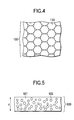
- Fig. 4 is a partly front view of the micro lens array 100 in the case where the bottom surface of each unit lens 110 is shaped like a circle.
- the transmittance of the optical sheet is reduced for the following reason.
- each unit lens 110 is a hexagonal shape rather than a circular shape. This is because in the case of a hexagonal shape, the unit lenses can be arranged to be closest packed without any gap so that the ratio of the area occupied by the unit lenses to the area of the surface for formation of the micro lens array can be made 100 % at maximum ideally.
- each unit lens when the shape of the bottom surface of each unit lens is a circular shape, the ratio of the area occupied by the unit lenses to the area of the surface for formation of the micro lens array is reduced to 90.7 % even in the case where the unit lenses are arranged to be closest packed without any gap, so that transmittance is reduced correspondingly by the reduction of the area ratio.
- the shape of the bottom surface of each unit lens is preferably a hexagonal shape from the point of view of increasing the ratio of the area occupied by the unit lenses to the area of the surface for formation of the micro lens array.
- Fig. 5 is a partly sectional view showing an example of the diffusing layer 500.
- the diffusing layer 500 contains a transparent medium 501 such as a transparent resin, and transparent fine particles 502 mixed with and dispersed into the transparent medium 501.
- the transparent medium 501 at least exhibits transparency to visible light.
- the transparent fine particles 502 are different in refractive index from the transparent medium 501 and at least exhibit transparency to visible light.
- thermoplastic transparent resin or a transparent resin having the function of an adhesive agent added to itself can be used as the transparent medium 501.
- an acrylic-based resin may be used preferably in terms of high transparency and durability.
- the transparent fine particles 502 are fine particles which are different in refractive index from the transparent medium 501 and which are transparent. Glass fine particles, silica fine particles, melamine-based fine particles, styrene-based fine particles, benzoguanamine-based fine particles or the like can be used as the transparent fine particles. Any shape such as a spherical shape, a ball gravel shape or a rectangular parallelepiped shape can be used as the shape of each of the transparent fine particles 502. Particularly, spherical fine particles capable of scattering light isotropically may be used preferably.
- the diffusing layer 500 has a function of scattering light incident on the diffusing layer 500 to thereby enlarge the viewing angle. There is however the possibility that the diffusing layer 500 may cause reduction of transmittance by disturbing the conformation of the positions of the opening portions 400 in the light absorbing layer to light condensed by the unit lenses 110 constituting the micro lens array 100.
- selecting the thickness d of the diffusing layer 500 to be as small as possible to eliminate the positional unconformity as sufficiently as possible is very effective in improving transmittance and minimizing the opening portions 400 in the light absorbing layer to suppress reflection of external light to thereby achieve high-contrast ratio display under the bright environment.
- the scattering sectional area ⁇ of the diffusing layer 500 is given by the expression (1): in which R is the particle radius of the transparent fine particles, N is the number density of the transparent fine particles, d is the thickness of the diffusing layer, and ⁇ n is the refractive index difference between the transparent medium and the transparent fine particles.
- ⁇ is the wavelength of light made incident on the diffusing layer 500.
- the strength of scattering is proportional to e ⁇ Nd
- the strength of scattering by the diffusing layer independently of the thickness d of the diffusing layer may be evaluated on the basis of the value of Q/R given by the expression (5).
- N is the number density of the transparent fine particles.
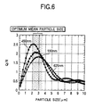
- Fig. 6 is a graph showing the relation between the particle size of the transparent fine particles in the diffusing layer of the optical sheet according to the invention and scattering characteristic.
- the light scattering characteristic of the diffusing layer increases exponentially as the value of Q/R increases.
- the reason why only the mean particle size is a subject of definition is that preparation of all fine particles having a predetermined particle size is not realistic because the particle size of the fine particles generally varies.
- the value of Q/R varies cyclically in accordance with the particle size and takes the maximum value at a first peak viewed in the increasing direction of the particle size.
- the values of Q/R vary in accordance with wavelengths and the particle size for maximizing the value of Q/R at wavelengths in a visible region has a certain range.
- transparent fine particles having a mean particle size in this range may be used preferably.
- Transparent fine particles having, as its mean particle size, a particle size for maximizing the value of Q/R in accordance with a wavelength range of from 525 to 575 nm high in relative luminous efficiency and preferably in accordance with a wavelength of 550 nm may be particularly preferably used because higher scattering characteristic can be obtained when observed by the human being.
- variation in the value of Q/R in accordance with wavelengths means variation in light scattering characteristic in accordance with colors. That is, in the particle size in which the value of Q/R varies widely in accordance with wavelengths, there is the possibility that image quality may be deteriorated by variation in color in accordance with angles of observation. Therefore, the mean particle size of the transparent fine particles is preferably selected from a particle size range which is as near a particle size for maximizing the value of Q/R as possible and in which variation in the value of Q/R in accordance with wavelengths is reduced in order to prevent image quality from being deteriorated by variation in color.
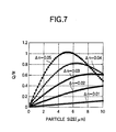
- Figs. 7 and 8 are graphs showing the relation between the particle size of the transparent fine particles and the scattering characteristic of the diffusing layer in the optical sheet according to the invention.
- Fig. 7 shows the relation between the particle size of the transparent fine particles and the value of Q/R in the case where ⁇ n changes in a range of from 0.01 to 0.05 with respect to light with a wavelength of 550 nm.
- Fig. 8 shows the relation between the particle size of the transparent fine particles and the value of Q/R in the case where ⁇ n changes in a range of from 0.05 to 0.20 with respect to light with a wavelength of 550 nm.
- the maximum value of Q/R doest not exist when the particle size range of the transparent fine particles is not larger than 10 ⁇ m.
- the value of Q/R is maximized when the particle size of the transparent fine particles is about 5 ⁇ m.
- the pitch of lenses in the micro lens array is preferably selected to be not larger than 100 ⁇ m, more preferably not larger than 50 ⁇ m.
- the thickness of the diffusing layer is as thin as possible compared with the lens pitch.
- the thickness of the diffusing layer is preferably selected to be not larger than 1/5 of the lens pitch.
- the thickness of the diffusing layer may be selected to be smaller than 20 ⁇ m, particularly not larger than 10 ⁇ m under the condition that sufficient scattering characteristic can be obtained in spite of the thickness of the diffusing layer.
- ⁇ n must be larger than 0.02.
- ⁇ n is preferably selected to be not smaller than 0.05 because the particle size of the transparent fine particles needs to be not larger than 5 ⁇ m.
- ⁇ n is preferably selected to be not smaller than 0.03 because the particle size of the transparent fine particles needs to be not larger than 10 ⁇ m.
- ⁇ n is advantageous because a thinner diffusing layer can be achieved and, at the same time, higher scattering characteristic can be obtained when transparent fine particles having a smaller particle size are used. Reduction in transmittance due to increase in reflection is, however, conspicuous if ⁇ n is larger than 0.2. Therefore, ⁇ n is preferably selected to be not larger than 0.2.
- a light absorbing layer 300 is formed on the diffusing layer 500.
- the light absorbing layer 300 has opening portions 400 located at focal points of the unit lenses 110 constituting the micro lens array 100 and located in corresponding positions near the focal points.
- the light absorbing layer 300 at least absorbs light with wavelengths in a visible region. That is, the light absorbing layer 300 has a function of absorbing external light incident on the optical sheet 30 from the environment to reduce reflection of the external light.
- the light absorbing layer 300 is preferably black.
- the light absorbing layer 300 can be made of a resin composition containing a known pigment or dye as an additive.
- fine opening portions 400 which are aligned with the unit lenses 110 constituting the micro lens array 100.
- a suitable technique selected from the various techniques in the related art can be used. Examples of the method for forming such fine patterns include: various kinds of printing techniques such as a screen printing method and an offset printing method; a photolithography technique using a light-sensitive resin such as a resist or a colored resist and a technique using the photolithography technique; and a technique using silver salt, diazo dye or the like.
- the unit lenses 110 constituting the micro lens array 100 need to be respectively, optically and accurately aligned with the opening portions 400 formed in the light absorbing layer in accordance with the unit lenses 110.
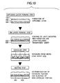
- Fig. 9 is an explanatory view showing an example of the method for producing the light absorbing layer in the optical sheet and the opening portions in the light absorbing layer.
- a diffusing layer 500 is formed on a rear surface of the transparent base material 200 having the micro lens array 100 formed on its front surface, by any one of these methods.
- the light-sensitive layer 310 containing a pigment or dye and functioning as a light absorbing layer is formed on the diffusing layer 500.
- the light-sensitive layer 310 may be made of a positive light-sensitive resin or may be made of a laminate of a light absorbing layer-forming material and a positive light-sensitive resin.
- the light-sensitive layer 310 is irradiated with light supposed to have a spread equal to that of image light incident on the optical sheet in practical use, or irradiated with substantially parallel light rays similar to the light in the condition that the micro lens array 100 is used as a substitute for a photomask, the light-sensitive layer 310 is exposed. On this occasion, portions of the light-sensitive layer 310 corresponding to the focal points of the unit lenses and their vicinity are selectively exposed on the basis of the light-condensing function of the unit lenses constituting the micro lens array 100.
- the selectively exposed portions are removed by development to thereby form opening portions 400.
- the other portions function as a light absorbing layer 300.
- a diffusing layer 500 is formed on a rear surface of the transparent base material 200 having the micro lens array 100 formed on its front surface, by any one of these methods.
- another transparent sheet 600 on which a light-sensitive and heat-sensitive layer 320 made of light-sensitive and heat-sensitive dye is formed in advance is stuck onto the diffusing layer 5.00 so that a surface of the transparent sheet 600 having the light-sensitive and heat-sensitive layer 320 formed thereon is brought into contact with the diffusing layer 500.
- the exposed portions of the light-sensitive and heat-sensitive layer 320 are achromatized to exhibit high transmittance.
- the non-exposed portions of the light-sensitive and heat-sensitive layer 320 are blacked when heated, so that the non-exposed portions function as a light absorbing layer.
- Diazo-based dye can be used as the material of the light-sensitive and heat-sensitive layer 320.
- the contrast ratio under the bright environment is reduced because of reduction in transmittance and increase in reflection of external light due to enlargement of the opening portions in the light absorbing layer in the same manner as in the case where the diffusing layer is made thick by the thickness of the unnecessary layer.
- an acrylic-based adhesive agent is used as the transparent medium contained in the diffusing layer 500 so that the diffusing layer 500 itself can function as an adhesive agent through which the diffusing layer 500 and the light-sensitive and heat-sensitive layer 320 are directly stuck onto each other.
- the light-sensitive and heat-sensitive layer 320 is irradiated with light supposed to have a spread equal to that of image light incident on the optical sheet in practical use, or irradiated with substantially parallel light rays similar to the light in the condition that the micro lens array 100 is used as a substitute for a photomask
- the light-sensitive and heat sensitive layer 320 is exposed.
- portions of the light-sensitive and heat-sensitive layer 320 corresponding to the focal points of the unit lenses and their vicinity are selectively exposed on the basis of the light-condensing function of the unit lenses constituting the micro lens array 100. Then, the light-sensitive and heat-sensitive layer 320 is heated.
- the non-exposed portions of the light-sensitive and heat-sensitive layer 320 are blacked so as to function as a light absorbing layer 300 whereas the selectively exposed portions of the light-sensitive and heat-sensitive layer 320 are achromatized and improved in transmittance so as to function as opening portions 400.
- unreacted nitrogen gas contained in the light-sensitive and heat-sensitive layer may be expanded as gas bubbles with a diameter of several millimeters to cause reduction in transmittance.
- generation of gas bubbles can be prevented when the heating process is carried out, for example, under a high pressure of from 2 X 10 5 to 5 X 10 5 Pa.
- this step it is unnecessary to use any developer. That is, this step is entirely performed in a dry process. Hence, there is an effect that productivity is high.
- Fig. 11 is a partly front view, from the light absorbing layer 300 side, of the optical sheet 30 in which the light absorbing layer having fine opening portions is formed by these methods.
- Fig. 11 corresponds to the case where the shape of the bottom surface of each of the unit lenses 110 is a hexagonal shape as shown in Fig. 3.
- the opening portions 400 in the light absorbing layer are arranged two-dimensionally in accordance with the arrangement of the unit lenses.
- the ratio of the longitudinal length h of the bottom surface of each unit lens 110 to the transverse length w thereof may be changed so that the longitudinal length h is larger than the transverse length w .
- each unit lens may be preferably shaped like a hexagon in order to increase the area occupied by the unit lenses in the surface for formation of the micro lens array.
- the interior angle ⁇ of a corner having the lowest interior angle in all corners in the shape of the bottom surface of each unit lens is not lower than 90 degrees, preferably not lower than 100 degrees. This is because transmittance is reduced if a corner having a low interior angle is present in each unit lens. That is, if a corner having a low interior angle is present in each unit lens, the curvature of the lens surface in the region of the corner and its vicinity is largely different from that in the other region. As a result, focal points are displaced, so that the unit lenses cannot function effectively.
- the ratio of the area occupied by the unit lenses to the area of the surface for formation of the micro lens array can be made 100 % theoretically in the same manner as in the case of a hexagonal shape.
- the interior angle in the shape of the bottom surface of each unit lens is not higher than 90 degrees, so that each unit lens has a portion not functioning as a lens effectively.
- the shape of the bottom surface in each of the unit lenses constituting the micro lens array is preferably selected as a hexagonal shape in order to maximize the ratio of the area occupied by the unit lenses to the area of the surface for formation of the micro lens array.
- the unit lens is deformed by pulling its side portions in order not to reduce the interior angle in the shape of the bottom surface of the unit lens as much as possible.
- the corner portions may be slightly rounded so that the shape of the bottom surface of each unit lens is not accurately a hexagonal shape.
- hexagonal shape used herein means a basically hexagonal shape, for example, including a hexagonal shape having rounded corners.
- a transparent sheet 600 may be further stuck onto the light absorbing layer 300 of the optical sheet 30 through a transparent adhesive agent so that the surface can be protected by the transparent sheet 600.
- a high-molecular film at least exhibiting transparency to visible light can be used as the transparent sheet 600.
- An acrylic plate having a thickness of several millimeters maybe used as the transparent sheet 600 so as to make the optical sheet itself have stiffness.
- An anti-reflection film may be further formed on the transparent sheet 600 in order to suppress reflection on the surface of the transparent sheet 600.
- a known technique may be used for forming the anti-reflection film. For example, there may be used a method of performing multi-coating with some kinds of metal oxides optically designed to be different in refractive index by vapor deposition or a method of applying a low-refractive-index material such as a fluorine compound.
- the optical sheet according to the invention is an optical sheet which can be used as a transmission type screen member in a back projection type display device or as a viewing angle enlarging member in a liquid-crystal display device and which is a member of the display device directly observed by the observer.
- the optical sheet is an important member whose performance has influence on the image quality of the display device.
- image light 1001 is incident on the surface of the optical sheet 30 where the micro lens array 100 is formed.
- the light incident on the micro lens array 100 suffers the refracting function of the unit lenses constituting the micro lens array 100, so that the light is made incident on the diffusing layer 500 while converged into positions corresponding to the opening portions 400 of the light absorbing layer 300.
- the light incident on the diffusing layer 500 passes through the diffusing layer 500 while scattered, and further passes through the opening portions 400 of the light absorbing layer 300 to the observer's side.
- the image light 1001 passing through the optical sheet 30 suffers the scattering function of the diffusing layer 500 as well as the refracting function of the unit lenses, so that a wider viewing angle can be achieved.
- the diffusing layer 500 has a small thickness of about several microns, sufficient scattering characteristic can be obtained.
- the lens pitch of the micro lens array has a small value of tens of microns to meet high-precision display, the size of each of the opening portions 400 in the light absorbing layer 300 can be made small without sacrifice of transmittance.
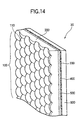
- Fig. 14 is a partly perspective view of an optical sheet according to this embodiment.
- a photo resist is applied on a planar substrate and exposed and developed through a photomask having patterns formed correspondingly to the shapes of the bottom surfaces of the unit lenses to thereby obtain a photo resist pattern in which fine equilateral hexagonal columns are arrayed.
- the photo resist pattern is heated to thereby obtain a photo resist pattern in which substantially dome-like fine lens shapes each having a bottom surface shaped like an equilateral hexagon are arrayed on the basis of surface tension at melting.
- an Ni film as an undercoat film is first formed on a surface of the photo resist pattern by sputtering and further plated with Ni by about 0.3 mm, the Ni layer is released from the photo resist pattern to thereby obtain an Ni stamper.
- a micro lens array shape is directly formed on the transparent base material 200 of a triacetyl cellulose film 50 ⁇ m thick initially by a vacuum hot pressing method using the Ni stamper.
- an integrally molded piece of the micro lens array 100 and the transparent base material 200 is obtained.
- a diffusing layer about 8 ⁇ m thick is formed on a rear surface of the transparent base material 200 opposite to the surface for formation of the micro lens array.
- Amixture of a transparent medium made of an acrylic-based transparent adhesive agent having a refractive index of 1.47 with benzoguanamine-based transparent fine particles having a mean particle size of 2.5 ⁇ m and a refractive index of 1.57 is used as the material of the diffusing layer 500.
- the adhesive property of the transparent medium is used so that the diffusing layer 500 adheres to the transparent base material 200.
- the particle size of the transparent fine particles is in a particle size range for maximizing the value of Q/R in accordance with wavelengths in a visible region, so that high light scattering can be obtained even in the case where the diffusing layer 500 is thin.
- a light-sensitive material is applied on the diffusing layer 500.
- the light-sensitive material is exposed to and processed by light supposed to have a spread equal to that of image light incident on the optical sheet in practical use or exposed to substantially parallel light rays similar to the light in the condition that the micro lens array 100 is used as a substitute for a photomask.
- a light absorbing layer 300 having opening portions 400 which are formed so as to be self-aligned at focal points of the unit lenses 110 and in positions near the focal points.
- the transparent sheet 600 made of a triacetyl cellulose film is bonded as a protective member onto the light absorbing layer 300 through an acrylic-based transparent adhesive agent.
- the diffusing layer 500 has a small thickness of 8 ⁇ m, sufficient scattering characteristic can be obtained.
- an optical sheet which has such a wide viewing angle that the angle for reducing luminance both in the horizontal direction and in the vertical direction to a half of frontal luminance is 60 degrees.
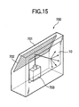
- Fig. 15 is a schematic perspective view of a back projection type display device using the optical sheet according to the invention.
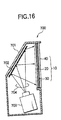
- Fig. 16 is a schematic sectional view of the back projection type display device.
- the projection type display device 700 according to the invention has a housing 701, a projector 703 disposed in the housing 701, a reflecting mirror 702 disposed in the housing 701, and a transmission type screen 10. Image light 704 emitted from the projector 703 is projected onto the transmission type screen 10 through the reflecting mirror 702, so that an image is displayed.
- Amirror obtained by vapor-depositing a reflective metal such as silver or aluminum on optically isotropic transparent glass can be used as the reflecting mirror 702.
- a liquid-crystal projector can be used as the projector 703.
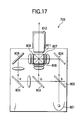
- Fig. 17 is a schematic sectional view of a liquid-crystal projector used in the back projection type display device according to this embodiment.
- the liquid-crystal projector has a light source 801, liquid-crystal display elements 807, 808 and 809 as two-dimensional optical switching elements, color-separating dichroic mirrors 802 and 803, a color-synchronizing cross-dichroicprism 811, total reflection mirrors 804, 805 and 806, and a projecting lens set 810.
- the light source 801 has a reflector shaped like a paraboloid of revolution or an ellipsoid of revolution, and a white light source such as a xenon lamp or a metal halide lamp.
- a white light source such as a xenon lamp or a metal halide lamp.
- the white light incident on the color-separating dichroic mirror 802 is separated into blue light (B) and other light by the color-separating dichroic mirror 802.
- the blue light (B) is reflected by the total reflection mirror 804 and then reaches the liquid-crystal display element 807.
- the other reflected light than the blue light (B) is further separated into green light (G) and red light (R) by the color-separating dichroic mirror 803.
- the green light (G) reaches the liquid-crystal display element 808.
- the red light (R) is reflected by the total reflection mirrors 805 and 806 and then reaches the liquid-crystal display element 809.
- TN liquid-crystal display elements can be used as the liquid-crystal display elements 807, 808 and 809.
- the color light beams incident on the liquid-crystal display devices respectively are spatially modulated in accordance with image information and then emitted from the liquid-crystal display devices respectively.
- the color light beams modulated by the liquid-crystal display elements respectively enter the color-synchronizing cross-dichroic prism 811. After synchronization, the-resulting light is projected onto the transmission type screen 10 through the projecting lens set 810.
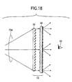
- the transmission type screen 10 has an optical sheet 30, and a Fresnel lens sheet 20.
- the optical sheet 30 and the Fresnel lens sheet 20 are arranged in order of view from the side of the observer 50.
- a transparent acrylic plate 40 about 2 mm thick may be disposed on a front surface side of the optical sheet 30 so that the optical sheet 30 can be protected by the transparent acrylic plate 40.
- the Fresnel lens sheet 20 is an optical component which has the same function as that of a convex lens. That is, the Fresnel lens sheet 20 has a function of collimating image light 704 emitted from the projector 703 to thereby change the incidence angle of light incident on the optical sheet 30 to zero degrees or its vicinity.
- Fig. 19 is a graph showing an example of the relation of luminance and viewing angle characteristic in the back projection type display device according to the invention.
- Fig. 19 shows results of measurement in terms of the relation of luminance and viewing angle characteristic both in the horizontal direction and in the vertical direction.
- the vertical axis shows relative luminance standardizedwith reference to frontal luminance (at an emission angle of 0 degrees), and the horizontal axis shows an emission angle both in the vertical direction and in the horizontal direction.
- results of measurement in the case where a related-art lenticular lens sheet is used are also shown in Fig. 19.
- a wide viewing angle both in the horizontal direction and in the vertical direction can be obtained on the basis of the function of the diffusing layer of the optical sheet compared with the case where the related-art lenticular lens sheet is used.
- the viewing angle in the vertical direction becomes as wide as the viewing angle in the horizontal direction because of use of the unit lenses each having a bottom surface shaped like an equilateral hexagon whereas the viewing angle in the vertical direction is narrow in the related-art lenticular lens sheet.
- low-luminance black display can be achieved even under the bright environment because a large part of external light incident on the transmission type screen 10 is absorbed to the light absorbing layer of the optical sheet 30.
- high-resolution high-quality display can be achieved because the lens pitch of the micro lens array has a small value of tens of microns to display pixels clearly.
- the back projection type display device has wide viewing angle characteristic because the lens-pitch of the-optical sheet 30 used as the transmission type screen 10 has a small value of tens of microns, so that the display device is bright even when viewed from any angle.
- the back projection type display device further has high-precision, high-luminance wide viewing angle characteristic because it has a high effect in reducing unnecessary external light.
- the back projection type display device further has high-contrast-ratio high-quality image display characteristic because low-luminance black display can be achieved even under the bright environment.
- Fig. 20 is a partly schematic sectional view of a direct-vision liquid-crystal display device according to this embodiment.
- the direct-vision liquid-crystal display device has a liquid-crystal display element 910, a backlight unit 900 provided on the back of the liquid-crystal display element 910, and an optical sheet 30 provided in front of a polarizer 914 in the liquid-crystal display element 910.
- the backlight unit 900 can output substantially parallel light rays efficiently.
- a "backlight assembly for electronic optical display" described in International Unexamined Japanese Patent Publication No. Hei. 9-505412 and International Patent Publication WO95/14255 can be used as the backlight unit 900.
- the backlight unit 900 used herein has a light source 901 made of a cold-cathode tube, a light pipe 902 made of a transparent acrylic resin, and a collimator element 903.
- a known element can be used as the collimator element 903.
- a combination of a quadrangular pyramid-shaped micro tapered rod array and a lens array optically coupled with the micro tapered rod array can be used as the collimator element 903 on the light pipe 902.
- light guided by the light pipe 902 is propagated through micro tapered rods while totally reflected once or a plurality of times by wall surfaces of the micro tapered rods. After the light is collimated by the refracting function of the lens array, the light emits as substantially parallel light rays from the lens array.
- any other element such as a micro prism sheet or a micro lens array may be used as the collimator element 903.
- illumination light rays which are made substantially parallel in a half-value angle range of ⁇ 10 degrees can be obtained.
- the liquid-crystal display element 910 has a first transparent substrate 918, a second transparent substrate 912, and a liquid-crystal layer 916.
- the first transparent substrate 918 has a transparent electrode 917 of ITO (Indium Tin Oxide), and an oriented film of a polyimide-based high-molecular compound.
- the second transparent substrate 912 has an oriented film not shown, transparent electrodes 915 for forming pixels, and switching elements such as wiring and thin-film transistors not shown but connected to the transparent electrodes 915.
- the liquid-crystal layer 916 is made of nematic liquid crystal which is enclosed between the two transparent substrates 912 and 918 connected to each other through a sealing agent 913 and which is positive in induced anisotropy.
- liquid-crystal display element 910 the oriented films applied on the two transparent substrates 912 and 918 respectively are rubbed to form a so-called TN liquid-crystal display element in which the major axes of liquid-crystal molecules in the liquid-crystal layer 916 are continuously twisted by 90 degrees between the two transparent substrates.
- Polarizers 911 and 914 are disposed on the rear surface side of the second transparent substrate 912 and on the front surface side of the first transparent substrate 918 respectively in the liquid-crystal display element 910 so that linearly polarized light beams perpendicular to each other are transmitted through the polarizers 911 and 914 respectively.
- a plate having a stretched film of polyvinyl alcohol formed to have a polarizing function by absorbing iodine to the stretched film, andTAC (TriAcetyl Cellulose) protective layers applied on opposite surfaces of the stretched film is used as each of the polarizers 911 and 914.
- Each of the polarizers 911 and 914 is bonded to corresponding one of the transparent substrates 912 and 918 through an acrylic-based adhesive agent.
- An optical sheet 30 is disposed on the front surface of the liquid-crystal display element 910.
- An optical sheet described in the "Embodiment of Optical Sheet” is used as the optical sheet.
- the bonding of the optical sheet 30 and the liquid-crystal display element 910 may be fixed by an adhesive agent 35 applied in a frame shape to surround the circumferential edge portion of the liquid-crystal display element 910.
- the liquid-crystal display element 910 and the optical sheet 30 may be pressed by a frame not shown so as to be fixed to each other without bonding.
- the operation of the direct-vision liquid-crystal display device will be described below.
- linearly polarized light transmitted through the polarizer 911 is transmitted through the liquid-crystal layer 916 so as to be made incident on the polarizer 914.
- the state of polarization of light passing through the liquid-crystal layer 916 varies in accordance with the electric field applied on the liquid-crystal layer 916. Therefore, voltages corresponding to image information are applied to electrodes corresponding to pixels so that an image is formed while the quantity of light transmitted through the polarizer 914 is controlled.
- the image light transmitted through the polarizer 914 is made incident on the optical sheet 30.
- a large part of the light incident on the optical sheet 30 is made incident on the unit lenses constituting the micro lens array.
- the light incident on the unit lenses is made incident on the diffusing layer while the light is converged into positions corresponding to the opening portions of the light absorbing layer by the refracting function of the unit lenses.
- the light incident on the diffusing layer passes through the diffusing layer while scattered, and further passes through the opening portions of the light absorbing layer to the observer 50 side.
- the TN liquid-crystal display device has viewing angle dependence.
- lowering of contrast ratio, inversion of gradation and change of chromaticity occur. Accordingly, good image quality can be obtained only in a limited angle range near the front direction.
- the percentage of light in an angle range allowing good image quality to be obtained in the liquid-crystal display element 910 is high because substantially parallel light rays are emitted from the backlight unit 900 toward the liquid-crystal display element 910.
- light-utilizing efficiency is high because light loss in the optical sheet 30 is reduced. Hence, a high-luminance image can be obtained.
- a high-luminance high-contrast image can be obtained without change of chromaticity and without inversion of gradation in a wide viewing angle range.
- the optical sheet 30 has a high effect in reducing external light, low-luminance black display can be achieved even under the bright environment so that a high-contrast-ratio image can be obtained.
- the liquid-crystal display device according to the invention When the liquid-crystal display device according to the invention is evaluated, the liquid-crystal display device having a contrast ratio of 80:1 or higher, isotropy and a wide viewing angle is obtained without change of chromaticity and without inversion of gradation in a viewing angle range of ⁇ 80 degrees.
- the display mode is not limited to the TN mode.
- a VA Vertical Aligned
- an ECB Electro Mechanical Controlled Birefringence
- an OCB Optically Compensated Bend
- STN Super Twisted Nematic
- a passive matrix drive method as well as an active matrix drive method using switching elements such as thin-film transistors may be used as the drive method.
- the lens pitch of the micro lens array can be reduced to a small value of tens of microns so that high-precision image display can be achieved.
- a diffusing layer can be provided so that sufficient light scattering performance can be obtained even in the case where the diffusing layer is thin.
- the optical sheet can be obtained as an optical sheet wide in viewing angle, high in transmittance, small in size of opening portions of the light absorbing layer and low in external light reflectance.
- the image display device using the optical sheet according to the invention is high in precision, high in luminance and wide in viewing angle. Low-luminance black display can be achieved even under the bright environment. Hence, a high-contrast-ratio high-quality image can be obtained.
- the lens pitch in the optical sheet used as a transmission type screen has a small value of tens of microns.
- the display device has such wide viewing angle characteristic that it is bright even when viewed from any angle.
- reflection of external light is low, high precision, high luminance and wide viewing angle can be obtained.
- Low-luminances black display can be achieved even under the bright environment.
- a high-contrast-ratio high-quality image can be obtained.
- the optical sheet is disposed in front so that display having no change of chromaticity and no inversion of gradation can be obtained in a wide viewing angle range. Because the optical sheet used is highly effective in reducing reflection of external light, low-luminance black display can be achieved even under the bright environment. Hence, a high-contrast-ratio image can be obtained.
Landscapes
- Physics & Mathematics (AREA)
- General Physics & Mathematics (AREA)
- Optics & Photonics (AREA)
- Nonlinear Science (AREA)
- Chemical & Material Sciences (AREA)
- Mathematical Physics (AREA)
- Crystallography & Structural Chemistry (AREA)
- Engineering & Computer Science (AREA)
- Dispersion Chemistry (AREA)
- Manufacturing & Machinery (AREA)
- Optical Elements Other Than Lenses (AREA)
- Liquid Crystal (AREA)
- Overhead Projectors And Projection Screens (AREA)
- Devices For Indicating Variable Information By Combining Individual Elements (AREA)
- Projection Apparatus (AREA)
- Transforming Electric Information Into Light Information (AREA)
Abstract
Description

Claims (9)
- An optical sheet comprising:wherein said diffusing layer is made of a transparent medium containing transparent fine particles different in refractive index from said transparent medium, anda transparent base material;a fine lens array constituted by a plurality of fine unit lenses formed on a front surface of said transparent base material;a diffusing layer formed on a rear surface of said transparent base material opposite to said surface on which said fine lens array is formed; anda light absorbing layer formed on said diffusing layer and including fine opening portions substantially located at focal points of said unit lenses;said transparent fine particles have a mean particle size in a particle size range for maximizing a value of Q/R at each of wavelengths in a visible region when Q is a scattering sectional area per transparent fine particle, and R is a radius of each of said transparent fine particles.
- An optical sheet according to claim 1, wherein said transparent fine particles have a mean particle size in a particle size range for maximizing a value of Q/R in a wavelength range of from 525 to 575 nm.
- An optical sheet comprising:wherein said diffusing layer is made of a transparent medium containing transparent fine particles different in refractive index from said transparent medium, anda transparent base material;a fine lens array constituted by a plurality of fine unit lenses formed on a front surface of said transparent base material;a diffusing layer formed on a rear surface of said transparent base material opposite to said surface on which said fine lens array is formed; anda light absorbing layer formed on said diffusing layer and including fine opening portions substantially located at focal points of said unit lenses;said transparent fine particles have a mean particle size in one range selected from a particle size range for maximizing a value of Q/R at each of wavelengths in a visible region and a range which is near said particle size range and in which variation in the value of Q/R due to the wavelengths in the visible region is reduced, when Q is a scattering sectional area per transparent fine particle, and R is a radius of each of said transparent fine particles.
- An optical sheet according to claim 1, wherein said unit lenses constituting said fine lens array are arranged at intervals of a pitch of not larger than 10 µm, Δn is in a range of from 0.03 to 0.2 when Δn is the refractive index difference between said transparent medium and said transparent fine particles, and said diffusing layer has a thickness smaller than 20 µm.
- An optical sheet comprising:wherein each of bottom surfaces of said unit lenses constituting said fine lens array is basically shaped like a hexagon so that said unit lenses are arranged so as to be closest packed.a transparent base material;a fine lens array constituted by a plurality of fine unit lenses formed on a front surface of said transparent base material; anda light absorbing layer formed on a rear surface of said transparent base material opposite to said surface on which said fine lens array is formed, said light absorbing layer. including fine opening portions substantially located at focal points of said unit lenses;
- An optical sheet according to claim 5, wherein interior angles of the shape of said bottom surface in each of said unit lenses are all not lower than 90 degrees.
- An optical sheet according to claim 5, wherein a longitudinal length of the shape of said bottom surface in each of said unit lenses is longer than a transverse length thereof.
- A back projection type display device comprising:wherein said diffusing layer of said optical sheet is made of a transparent medium containing transparent fine particles different in refractive index from said transparent medium, and said transparent fine particles have a mean particle size in one range selected from a particle size range for maximizing a value of Q/R at each of wavelengths in a visible region and a range which is near said particle size range and in which variation in the value of Q/R due to the wavelengths in the visible region is reduced, when Q is a scattering sectional area per transparent fine particle, and R is a radius of each of said transparent fine particles.a projector including a light source, a two-dimensional optical switching element for modulating light emitted from said light source in accordance with image information to form an optical image, and a projection lens for projecting said optical image while magnifying said optical image; anda transmission type screen having a back surface for receiving light projected from said projector, and a front surface for displaying said light, said transmission type screen including an optical sheet, and a Fresnel lens sheet provided on a projection light incidence side of said optical sheet, said optical sheet having a transparent base material, a fine lens array constituted by a plurality of fine unit lenses formed on a front surface of said transparent base material, a diffusing layer formed on a rear surface of said transparent base material opposite to said surface on which said fine lens array is formed, and a light absorbing layer formed on said diffusing layer and having fine opening portions substantially located at focal points of said unit lenses;
- A liquid-crystal display device comprising:wherein said liquid-crystal display device further comprises a backlight unit disposed on a back surface side of said pair of transparent substrates for outputting substantially parallel light rays, and an optical sheet disposed on a light emitting surface side of said pair of transparent substrates, said optical sheet including a transparent base material, a fine lens array constituted by a plurality of fine unit lenses formed on a front surface of said transparent base material, a diffusing layer formed on a rear surface of said transparent base material opposite to said surface on which said fine lens array is formed, and a light absorbing layer formed on said diffusing layer and having fine opening portions substantially located at focal points of said unit lenses;a pair of transparent substrates each of which is constituted by a laminate of a transparent electrode and an oriented film and which are bonded to each other through a predetermined gap so that surfaces on which said oriented films are formed are opposite to each other;a liquid-crystal layer held between said pair of transparent substrates;a unit for applying a voltage corresponding to an image signal between said transparent electrodes; andpolarizers arranged on a light incidence surface side and a light emitting surface side of said pair of transparent substrates respectively;said diffusing layer of said optical sheet is made of a transparent medium containing transparent fine particles different in refractive index from said transparent medium; andsaid transparent fine particles have a mean particle size in one range selected from a particle size range for maximizing a value of Q/R at each of wavelengths in a visible region and a range which is near said particle size range and in which variation in the value of Q/R due to the wavelengths in the visible region is reduced, when Q is a scattering sectional area per transparent fine particle, and R is a radius of each of said transparent fine particles.
Priority Applications (1)
| Application Number | Priority Date | Filing Date | Title |
|---|---|---|---|
| EP08016475A EP1998191A3 (en) | 2001-10-11 | 2002-10-10 | Optical sheet and display device having the optical sheet |
Applications Claiming Priority (2)
| Application Number | Priority Date | Filing Date | Title |
|---|---|---|---|
| JP2001313983 | 2001-10-11 | ||
| JP2001313983A JP2003121609A (en) | 2001-10-11 | 2001-10-11 | Optical sheet and display device having the same |
Related Child Applications (1)
| Application Number | Title | Priority Date | Filing Date |
|---|---|---|---|
| EP08016475A Division EP1998191A3 (en) | 2001-10-11 | 2002-10-10 | Optical sheet and display device having the optical sheet |
Publications (2)
| Publication Number | Publication Date |
|---|---|
| EP1302787A2 true EP1302787A2 (en) | 2003-04-16 |
| EP1302787A3 EP1302787A3 (en) | 2004-02-25 |
Family
ID=19132366
Family Applications (2)
| Application Number | Title | Priority Date | Filing Date |
|---|---|---|---|
| EP02022929A Ceased EP1302787A3 (en) | 2001-10-11 | 2002-10-10 | Optical sheet and display device having the optical sheet |
| EP08016475A Withdrawn EP1998191A3 (en) | 2001-10-11 | 2002-10-10 | Optical sheet and display device having the optical sheet |
Family Applications After (1)
| Application Number | Title | Priority Date | Filing Date |
|---|---|---|---|
| EP08016475A Withdrawn EP1998191A3 (en) | 2001-10-11 | 2002-10-10 | Optical sheet and display device having the optical sheet |
Country Status (5)
| Country | Link |
|---|---|
| US (1) | US6822707B2 (en) |
| EP (2) | EP1302787A3 (en) |
| JP (1) | JP2003121609A (en) |
| KR (2) | KR100854223B1 (en) |
| TW (1) | TW561278B (en) |
Cited By (15)
| Publication number | Priority date | Publication date | Assignee | Title |
|---|---|---|---|---|
| EP1617285A1 (en) * | 2004-07-14 | 2006-01-18 | Seiko Epson Corporation | Screen and projector |
| EP1970751A1 (en) * | 2007-03-15 | 2008-09-17 | LG Electronics Inc. | Optical sheet and liquid crystal display device having the same |
| CN1885129B (en) * | 2005-06-20 | 2010-08-18 | 日立麦克赛尔株式会社 | Lighting devices and display devices |
| WO2010130313A3 (en) * | 2009-05-15 | 2011-01-06 | Fraunhofer-Gesellschaft zur Förderung der angewandten Forschung e.V. | Device for projecting images |
| WO2011123429A2 (en) | 2010-04-01 | 2011-10-06 | Microsoft Corporation | Enhanced viewing brightness for surface display |
| WO2012040797A1 (en) * | 2010-10-01 | 2012-04-05 | Barco N.V. | Curved back-projection screen |
| EP2107966A4 (en) * | 2007-02-02 | 2012-12-12 | Arkema France | Multi-layer screen composites |
| TWI398672B (en) * | 2004-07-22 | 2013-06-11 | 薩比克創新塑膠有限公司 | Light collimating and diffusing film and system for manufacturing the same |
| WO2013114162A1 (en) * | 2012-01-30 | 2013-08-08 | Sony Mobile Communications Ab | Electronic display projection assembly having substantially white off state |
| KR20180133924A (en) * | 2016-04-27 | 2018-12-17 | 주식회사 쿠라레 | Diffuser plate and projection projector device |
| US10288995B2 (en) | 2017-06-15 | 2019-05-14 | Esterline Belgium Bvba | Aspherical dome display and method of rear projection |
| CN110998383A (en) * | 2018-07-26 | 2020-04-10 | 迪睿合株式会社 | Polarizing plate and optical device |
| CN111077722A (en) * | 2018-10-18 | 2020-04-28 | 深圳光峰科技股份有限公司 | Projection screen and processing method thereof |
| CN119087732A (en) * | 2024-10-25 | 2024-12-06 | 东莞市尺度电子科技有限公司 | A projection film structure for projecting grayscale patterns and a projection film production method |
| US12710581B2 (en) | 2023-09-23 | 2026-08-18 | S.V.V. Technology Innovations, Inc. | Thin and flexible edge-lit waveguide illumination systems with complex surface topologies and light converting properties |
Families Citing this family (87)
| Publication number | Priority date | Publication date | Assignee | Title |
|---|---|---|---|---|
| JP2002311211A (en) * | 2001-04-18 | 2002-10-23 | Dainippon Printing Co Ltd | Lens sheet and manufacturing method thereof |
| CA2417925A1 (en) * | 2001-06-01 | 2003-01-30 | Toppan Printing Co., Ltd. | Micro-lens sheet and projection screen |
| JP4194809B2 (en) * | 2002-08-21 | 2008-12-10 | フジノン株式会社 | Micro lens array molding equipment |
| KR100480730B1 (en) * | 2003-03-03 | 2005-04-07 | 엘지전자 주식회사 | A Display Apparatus for Three Dimensional Image |
| TW200417789A (en) * | 2003-03-14 | 2004-09-16 | Hon Hai Prec Ind Co Ltd | Backlight module and diffuser plate used therein |
| JP4912562B2 (en) * | 2003-04-22 | 2012-04-11 | シャープ株式会社 | Liquid crystal display device and television receiver |
| CN100456100C (en) * | 2003-06-20 | 2009-01-28 | 卡西欧计算机株式会社 | Display device and manufacturing method thereof |
| JP4202221B2 (en) * | 2003-09-26 | 2008-12-24 | シャープ株式会社 | Photorefractive element array substrate, image display element, and image display apparatus |
| GB0322681D0 (en) * | 2003-09-27 | 2003-10-29 | Koninkl Philips Electronics Nv | Multi-view display |
| US20070253051A1 (en) * | 2003-09-29 | 2007-11-01 | Kunihiko Ishihara | Optical Device |
| JP2005141202A (en) | 2003-11-03 | 2005-06-02 | Arisawa Mfg Co Ltd | Transmission screen |
| JP3818289B2 (en) | 2003-11-18 | 2006-09-06 | セイコーエプソン株式会社 | Transmission screen and rear projection display device |
| KR100971956B1 (en) * | 2003-12-26 | 2010-07-23 | 엘지디스플레이 주식회사 | Direct type backlight unit and liquid crystal display device using the same |
| JP2005221619A (en) * | 2004-02-04 | 2005-08-18 | Toppan Printing Co Ltd | Optical sheet, backlight, and liquid crystal display device |
| US20070177263A1 (en) * | 2004-07-23 | 2007-08-02 | Kuraray Co. Ltd | Back projection-type screen and back projection-type projection device |
| JP2006126312A (en) | 2004-10-27 | 2006-05-18 | Seiko Epson Corp | Screen, screen manufacturing method and projector |
| EP1845394B1 (en) * | 2005-01-31 | 2011-12-28 | Toppan Printing Co., Ltd. | Optical sheet, and backlight unit and display using the same |
| KR100804191B1 (en) * | 2005-04-08 | 2008-02-18 | 엘지전자 주식회사 | Semi-transmissive liquid crystal panel and its manufacturing method |
| US7755263B2 (en) * | 2005-05-04 | 2010-07-13 | Samsung Corning Precision Glass Co., Ltd. | External light-shielding layer, filter for display device including the external light-shielding layer and display device including the filter |
| JP4792813B2 (en) * | 2005-05-24 | 2011-10-12 | 凸版印刷株式会社 | Optical sheet, optical sheet and backlight unit |
| JP2006350177A (en) * | 2005-06-20 | 2006-12-28 | Seiko Epson Corp | Optical sheet manufacturing method, optical sheet, planar illumination device, electro-optical device |
| JP2007033597A (en) * | 2005-07-25 | 2007-02-08 | Seiko Epson Corp | Optical sheet, backlight unit, electro-optical device, electronic apparatus, optical sheet manufacturing method, and optical sheet cutting method |
| EP1914066B1 (en) | 2005-08-09 | 2016-09-07 | Asahi Glass Company, Limited | Thin sheet glass laminate and method for manufacturing display using thin sheet glass laminate |
| JP4876519B2 (en) * | 2005-10-06 | 2012-02-15 | セイコーエプソン株式会社 | Lens substrate manufacturing method, lens substrate, transmissive screen, and rear projector |
| CN100416369C (en) * | 2005-10-13 | 2008-09-03 | 长兴化学工业股份有限公司 | Light-gathering sheet |
| JP4835165B2 (en) * | 2006-01-18 | 2011-12-14 | 日立化成工業株式会社 | Method for forming opening of diffuse reflection layer having metal reflection film |
| KR101287208B1 (en) * | 2006-06-30 | 2013-07-16 | 전북대학교산학협력단 | Liquid Crystal Display Device |
| KR100820773B1 (en) * | 2006-08-18 | 2008-04-10 | 신화인터텍 주식회사 | Diffusion sheet, backlight assembly and liquid crystal display including the same |
| US7483215B2 (en) * | 2006-08-28 | 2009-01-27 | Genie Lens Technologies, Llc | Reflective imaging assembly for displaying interlaced images |
| TWM307132U (en) * | 2006-09-22 | 2007-03-01 | Eternal Chemical Co Ltd | Optic film |
| JP2008089906A (en) * | 2006-09-29 | 2008-04-17 | Toshiba Corp | Lens array unit and stereoscopic image display apparatus including the same |
| GB2444081B (en) | 2006-11-24 | 2011-05-11 | Ocuity Ltd | Manufacture of a birefringent liquid crystal component |
| JP4840105B2 (en) * | 2006-11-29 | 2011-12-21 | 凸版印刷株式会社 | Internal diffuser, polarizing plate including the same, and liquid crystal display device |
| JP5024992B2 (en) * | 2007-02-02 | 2012-09-12 | 株式会社ジャパンディスプレイセントラル | Display device |
| KR100817101B1 (en) * | 2007-04-04 | 2008-03-26 | 한국과학기술원 | Polymer or resist pattern, mold, metal thin film pattern, metal pattern and forming method using the same |
| KR101351886B1 (en) * | 2007-05-14 | 2014-01-17 | 엘지디스플레이 주식회사 | One-body multi functional optical sheet for liquid crystal display device |
| JP4935513B2 (en) * | 2007-06-06 | 2012-05-23 | ソニー株式会社 | OPTICAL ELEMENT AND ITS MANUFACTURING METHOD, OPTICAL ELEMENT MANUFACTURING REPLICATION BOARD AND ITS MANUFACTURING METHOD |
| KR100918034B1 (en) * | 2007-10-31 | 2009-09-18 | 제일모직주식회사 | Diffusion plate comprising an optical sheet having a reflecting portion on the back and an optical sheet having a lenticular lens on the front |
| US7609451B1 (en) * | 2008-02-05 | 2009-10-27 | Serigraph, Inc. | Printed article for displaying images having improved definition and depth |
| US8177408B1 (en) * | 2008-02-15 | 2012-05-15 | Fusion Optix, Inc. | Light filtering directional control element and light fixture incorporating the same |
| JP4518178B2 (en) * | 2008-04-15 | 2010-08-04 | ソニー株式会社 | Lens array sheet, optical member, light source, and liquid crystal display device |
| JP4518179B2 (en) * | 2008-04-15 | 2010-08-04 | ソニー株式会社 | Lens array sheet, optical member, light source, and liquid crystal display device |
| WO2009128164A1 (en) * | 2008-04-17 | 2009-10-22 | 凸版印刷株式会社 | Optical device, uniform illumination device, optical sheet, backlight unit, and display unit |
| KR100989311B1 (en) * | 2008-05-15 | 2010-10-25 | 제일모직주식회사 | Optical laminated film for improving brightness |
| KR101034479B1 (en) * | 2008-07-07 | 2011-05-17 | 도레이첨단소재 주식회사 | Thin Film Transistor Liquid Crystal Display Optical Sheet for Backlight Unit and Thin Film Transistor Liquid Crystal Display |
| WO2010110432A1 (en) * | 2009-03-27 | 2010-09-30 | 日東電工株式会社 | Liquid crystal display device |
| US8162512B2 (en) * | 2009-09-10 | 2012-04-24 | Entire Technology Co., Ltd. | Optical sheet, manufacturing method thereof, and backlight assembly using the same |
| TWI392930B (en) | 2009-09-21 | 2013-04-11 | Coretronic Corp | Backlight module and liquid crystal display apparatus |
| TW201120486A (en) * | 2009-12-14 | 2011-06-16 | Coretronic Corp | Brightness enhancement film and backlight module |
| JP5322182B2 (en) * | 2010-05-14 | 2013-10-23 | Jx日鉱日石エネルギー株式会社 | MICRO LENS FOR ORGANIC EL ELEMENT, ORGANIC EL ELEMENT USING THE SAME, AND METHOD FOR PRODUCING THEM |
| JP5565771B2 (en) * | 2010-06-17 | 2014-08-06 | ルネサスエレクトロニクス株式会社 | Microlens manufacturing method and imaging device |
| US10121925B2 (en) * | 2010-06-18 | 2018-11-06 | University Of Florida Research Foundation, Inc. | Thin film photovoltaic devices with microlens arrays |
| US8928567B2 (en) * | 2010-08-31 | 2015-01-06 | Sharp Laboratories Of America, Inc. | Switchable viewing angle display |
| US8947333B2 (en) * | 2010-08-31 | 2015-02-03 | Sharp Laboratories Of America, Inc. | Switchable viewing angle display with local dimming function |
| JP5730521B2 (en) * | 2010-09-08 | 2015-06-10 | 株式会社日立ハイテクノロジーズ | Heat treatment equipment |
| US9891098B2 (en) * | 2010-12-30 | 2018-02-13 | Apple Inc. | Diffuser and filter structures for light sensors |
| US8665244B2 (en) * | 2011-02-22 | 2014-03-04 | Microsoft Corporation | Optical touch detection |
| US8553168B2 (en) * | 2011-04-27 | 2013-10-08 | Finity Labs | Optical film for increasing the viewing angle of liquid crystal display devices |
| JP2013068872A (en) * | 2011-09-26 | 2013-04-18 | Goyo Paper Working Co Ltd | Lens sheet and el light-emitting device |
| US20130169900A1 (en) * | 2012-01-02 | 2013-07-04 | Microsoft Corporation | Non-Optically Bonded Display Device |
| CN104364703B (en) * | 2012-06-12 | 2017-05-03 | 英派尔科技开发有限公司 | Display structure with transmittance controllable layer |
| JP2014077883A (en) * | 2012-10-10 | 2014-05-01 | Dainippon Printing Co Ltd | Reflection screen, video display system |
| JP6102194B2 (en) * | 2012-11-09 | 2017-03-29 | 船井電機株式会社 | Projector and projection screen |
| TW201504728A (en) * | 2013-07-31 | 2015-02-01 | 鴻海精密工業股份有限公司 | Backlight module |
| CN104460214B (en) * | 2013-09-18 | 2018-01-30 | 深圳市东方硅源科技有限公司 | Optical glass |
| TWI479194B (en) * | 2014-02-06 | 2015-04-01 | Benq Materials Corp | Light switching module |
| KR101433023B1 (en) * | 2014-03-11 | 2014-08-25 | 에스케이씨하스디스플레이필름(유) | Optical sheet |
| CN106033159B (en) | 2015-03-12 | 2019-10-01 | 中强光电股份有限公司 | Display device |
| CN106033156B (en) | 2015-03-12 | 2019-11-05 | 中强光电股份有限公司 | Display device and display method |
| CN105042407A (en) * | 2015-06-24 | 2015-11-11 | 南京中电熊猫液晶显示科技有限公司 | Direct-type LED (Light-Emitting Diode) backlight unit |
| TWI579635B (en) * | 2015-12-28 | 2017-04-21 | 中強光電股份有限公司 | Projection system and screen thereof |
| KR20170134148A (en) * | 2016-05-27 | 2017-12-06 | 이용희 | Case with 3d film |
| JP2018115923A (en) * | 2017-01-17 | 2018-07-26 | 株式会社エンプラス | Marker |
| KR101951123B1 (en) * | 2017-10-17 | 2019-02-21 | 인하대학교 산학협력단 | Retro-reflect micro mirror array including parabolic surface |
| EP3502554A1 (en) * | 2017-12-20 | 2019-06-26 | ZKW Group GmbH | Projection device for a motor vehicle headlight and method for the preparation of a projection device |
| CN107976727B (en) * | 2017-12-21 | 2024-05-14 | 深圳市光科全息技术有限公司 | LED image quality enhancement film |
| KR102554417B1 (en) * | 2018-06-18 | 2023-07-11 | 삼성전자주식회사 | Image sensor |
| CN211653677U (en) * | 2019-08-02 | 2020-10-09 | 神盾股份有限公司 | Fingerprint sensing module |
| CN110941036B (en) * | 2019-12-20 | 2022-05-03 | 宁波舜宇奥来技术有限公司 | Infrared light diffusion sheet |
| CN111025670B (en) * | 2019-12-20 | 2022-05-03 | 宁波舜宇奥来技术有限公司 | Infrared light diffusion sheet and optical system |
| CN111025839A (en) * | 2020-01-09 | 2020-04-17 | 成都菲斯特科技有限公司 | Orthographic projection screen and projection system |
| TWI921329B (en) * | 2020-03-31 | 2026-04-11 | 日商大日本印刷股份有限公司 | Diffusion components, manufacturing methods of diffusion components, surface light source devices, display devices, and dielectric multilayer films. |
| CN111458922A (en) * | 2020-04-08 | 2020-07-28 | 深圳市华星光电半导体显示技术有限公司 | Array substrate and manufacturing method thereof |
| KR102678171B1 (en) * | 2020-11-09 | 2024-06-26 | 주식회사 엘엠에스 | Optical sheet |
| CN112698432B (en) | 2020-12-31 | 2022-08-19 | 维沃移动通信有限公司 | Optical film, optical module and electronic equipment |
| CN113376925A (en) * | 2021-06-17 | 2021-09-10 | 纵深视觉科技(南京)有限责任公司 | Switchable optical function assembly and manufacturing method and manufacturing device thereof |
| CN120178558A (en) * | 2025-03-20 | 2025-06-20 | 武汉华星光电技术有限公司 | Backlight module and display module |
Family Cites Families (14)
| Publication number | Priority date | Publication date | Assignee | Title |
|---|---|---|---|---|
| JP2862571B2 (en) * | 1988-07-28 | 1999-03-03 | 株式会社東芝 | Transmissive liquid crystal display |
| JP2972271B2 (en) * | 1989-04-26 | 1999-11-08 | 株式会社日立製作所 | TRANSMISSION SCREEN AND METHOD OF MANUFACTURING SHEET-LIKE MEMBER USED FOR THE SAME, AND REAR PROJECTION DISPLAY USING THE SCREEN |
| GB2267579A (en) * | 1992-05-15 | 1993-12-08 | Sharp Kk | Optical device comprising facing lenticular or parallax screens of different pitch |
| US5598281A (en) | 1993-11-19 | 1997-01-28 | Alliedsignal Inc. | Backlight assembly for improved illumination employing tapered optical elements |
| JP2679642B2 (en) * | 1994-09-01 | 1997-11-19 | 日本電気株式会社 | Transmissive liquid crystal display |
| KR0163895B1 (en) * | 1995-01-06 | 1999-01-15 | 김광호 | LCD with improved viewing angle |
| JPH1039769A (en) | 1996-07-19 | 1998-02-13 | Toray Ind Inc | Micro lens array sheet |
| JPH10160911A (en) | 1996-12-05 | 1998-06-19 | Toppan Printing Co Ltd | Light diffusion layer for transmissive projection screen |
| JPH10260638A (en) | 1997-03-19 | 1998-09-29 | Asahi Chem Ind Co Ltd | Lenticular screen and its manufacture |
| JP3822961B2 (en) | 1997-09-11 | 2006-09-20 | 大日本印刷株式会社 | Lenticular lens sheet and transmissive screen |
| JP2001201611A (en) * | 2000-01-21 | 2001-07-27 | Hitachi Ltd | Optical functional sheet, planar light source using the same, and image display device |
| JP2001215501A (en) * | 2000-02-02 | 2001-08-10 | Fuji Photo Film Co Ltd | Lighting device and liquid crystal display device |
| US6897911B2 (en) | 2000-02-14 | 2005-05-24 | Fuji Photo Film Co., Ltd. | Light diffusing plate, liquid crystal display apparatus and rear projection apparatus |
| JP3456192B2 (en) | 2000-04-28 | 2003-10-14 | 株式会社デンソー | Wireless communication system |
-
2001
- 2001-10-11 JP JP2001313983A patent/JP2003121609A/en active Pending
-
2002
- 2002-10-08 US US10/265,769 patent/US6822707B2/en not_active Expired - Fee Related
- 2002-10-10 EP EP02022929A patent/EP1302787A3/en not_active Ceased
- 2002-10-10 EP EP08016475A patent/EP1998191A3/en not_active Withdrawn
- 2002-10-11 KR KR1020020062056A patent/KR100854223B1/en not_active Expired - Fee Related
- 2002-10-11 TW TW091123470A patent/TW561278B/en not_active IP Right Cessation
-
2008
- 2008-05-30 KR KR1020080050866A patent/KR20080064938A/en not_active Ceased
Cited By (24)
| Publication number | Priority date | Publication date | Assignee | Title |
|---|---|---|---|---|
| KR100729890B1 (en) * | 2004-07-14 | 2007-06-18 | 세이코 엡슨 가부시키가이샤 | Screen and projector |
| US7382534B2 (en) | 2004-07-14 | 2008-06-03 | Seiko Epson Corporation | Screen and projector with spherical lens array |
| EP1617285A1 (en) * | 2004-07-14 | 2006-01-18 | Seiko Epson Corporation | Screen and projector |
| TWI398672B (en) * | 2004-07-22 | 2013-06-11 | 薩比克創新塑膠有限公司 | Light collimating and diffusing film and system for manufacturing the same |
| CN1885129B (en) * | 2005-06-20 | 2010-08-18 | 日立麦克赛尔株式会社 | Lighting devices and display devices |
| EP2107966A4 (en) * | 2007-02-02 | 2012-12-12 | Arkema France | Multi-layer screen composites |
| EP1970751A1 (en) * | 2007-03-15 | 2008-09-17 | LG Electronics Inc. | Optical sheet and liquid crystal display device having the same |
| WO2010130313A3 (en) * | 2009-05-15 | 2011-01-06 | Fraunhofer-Gesellschaft zur Förderung der angewandten Forschung e.V. | Device for projecting images |
| WO2011123429A2 (en) | 2010-04-01 | 2011-10-06 | Microsoft Corporation | Enhanced viewing brightness for surface display |
| EP2553521A4 (en) * | 2010-04-01 | 2017-11-22 | Microsoft Technology Licensing, LLC | Enhanced viewing brightness for surface display |
| WO2012040797A1 (en) * | 2010-10-01 | 2012-04-05 | Barco N.V. | Curved back-projection screen |
| CN103250097A (en) * | 2010-10-01 | 2013-08-14 | 巴科股份有限公司 | curved rear projection screen |
| US9513541B2 (en) | 2010-10-01 | 2016-12-06 | Barco N.V. | Curved back-projection screen |
| CN103250097B (en) * | 2010-10-01 | 2015-09-16 | 巴科股份有限公司 | curved rear projection screen |
| US9063359B2 (en) | 2012-01-30 | 2015-06-23 | Sony Mobile Communications Ab | Electronic display projection assembly having substantially white off state |
| WO2013114162A1 (en) * | 2012-01-30 | 2013-08-08 | Sony Mobile Communications Ab | Electronic display projection assembly having substantially white off state |
| KR20180133924A (en) * | 2016-04-27 | 2018-12-17 | 주식회사 쿠라레 | Diffuser plate and projection projector device |
| US10288995B2 (en) | 2017-06-15 | 2019-05-14 | Esterline Belgium Bvba | Aspherical dome display and method of rear projection |
| CN110998383A (en) * | 2018-07-26 | 2020-04-10 | 迪睿合株式会社 | Polarizing plate and optical device |
| CN111077722A (en) * | 2018-10-18 | 2020-04-28 | 深圳光峰科技股份有限公司 | Projection screen and processing method thereof |
| CN111077722B (en) * | 2018-10-18 | 2022-03-25 | 深圳光峰科技股份有限公司 | Projection screen and processing method thereof |
| US11906891B2 (en) | 2018-10-18 | 2024-02-20 | Appotronics Corporation Limited | Projection screen and processing method therefor |
| US12710581B2 (en) | 2023-09-23 | 2026-08-18 | S.V.V. Technology Innovations, Inc. | Thin and flexible edge-lit waveguide illumination systems with complex surface topologies and light converting properties |
| CN119087732A (en) * | 2024-10-25 | 2024-12-06 | 东莞市尺度电子科技有限公司 | A projection film structure for projecting grayscale patterns and a projection film production method |
Also Published As
| Publication number | Publication date |
|---|---|
| EP1998191A3 (en) | 2010-07-28 |
| US6822707B2 (en) | 2004-11-23 |
| EP1302787A3 (en) | 2004-02-25 |
| KR20030030973A (en) | 2003-04-18 |
| KR100854223B1 (en) | 2008-08-25 |
| EP1998191A2 (en) | 2008-12-03 |
| JP2003121609A (en) | 2003-04-23 |
| KR20080064938A (en) | 2008-07-10 |
| TW561278B (en) | 2003-11-11 |
| US20030072080A1 (en) | 2003-04-17 |
Similar Documents
| Publication | Publication Date | Title |
|---|---|---|
| US6822707B2 (en) | Optical sheet and display device having the optical sheet | |
| KR100191482B1 (en) | Transmissive liquid crystal display with reduced dependence on display quality for vision | |
| US6784962B2 (en) | Method for fabricating a laminate film and method for fabricating a display device | |
| EP0760490B1 (en) | Image display apparatus | |
| US20040085611A1 (en) | Reflective display device and retro-reflector used therefor | |
| US7327519B2 (en) | Spatial light modulator and projector | |
| JP2000193984A (en) | Liquid crystal light valve device | |
| US20010015780A1 (en) | Light diffusing plate, liquid crystal display apparatus and rear projection apparatus | |
| JP3544349B2 (en) | Liquid crystal display | |
| JPH0772809A (en) | Microlens array sheet for liquid crystal display, and liquid crystal display using the same | |
| US10768430B2 (en) | Display device and head-mounted display | |
| JPH07120743A (en) | How to attach the microlens array sheet | |
| JPH0949925A (en) | Field-of-view film and liquid crystal display using the same | |
| EP0572996B1 (en) | Light valve apparatus and display system using the same | |
| JPH0743501A (en) | Microlens array sheet and liquid crystal display using the same | |
| JPH0743704A (en) | Liquid crystal display viewing angle expansion method | |
| JP3227802B2 (en) | Optical element for liquid crystal display and liquid crystal display using the same | |
| JPH0772808A (en) | Microlens array sheet and liquid crystal display using the same | |
| JPH09179113A (en) | Liquid crystal display | |
| JPH06347764A (en) | Display device | |
| JPH0764071A (en) | Microlens array sheet and liquid crystal display using the same | |
| JP2004013059A (en) | Liquid crystal display and electronic equipment | |
| JPH06242411A (en) | Light valve device and display device using it | |
| JPH0772810A (en) | Microlens array sheet and liquid crystal display using the same | |
| JPH1039287A (en) | Liquid crystal display |
Legal Events
| Date | Code | Title | Description |
|---|---|---|---|
| PUAI | Public reference made under article 153(3) epc to a published international application that has entered the european phase |
Free format text: ORIGINAL CODE: 0009012 |
|
| AK | Designated contracting states |
Designated state(s): AT BE BG CH CY CZ DE DK EE ES FI FR GB GR IE IT LI LU MC NL PT SE SK TR |
|
| AX | Request for extension of the european patent |
Extension state: AL LT LV MK RO SI |
|
| PUAL | Search report despatched |
Free format text: ORIGINAL CODE: 0009013 |
|
| RIC1 | Information provided on ipc code assigned before grant |
Ipc: 7G 02B 5/02 A |
|
| AK | Designated contracting states |
Kind code of ref document: A3 Designated state(s): AT BE BG CH CY CZ DE DK EE ES FI FR GB GR IE IT LI LU MC NL PT SE SK TR |
|
| AX | Request for extension of the european patent |
Extension state: AL LT LV MK RO SI |
|
| 17P | Request for examination filed |
Effective date: 20040622 |
|
| AKX | Designation fees paid |
Designated state(s): DE NL |
|
| 17Q | First examination report despatched |
Effective date: 20050317 |
|
| 17Q | First examination report despatched |
Effective date: 20050317 |
|
| STAA | Information on the status of an ep patent application or granted ep patent |
Free format text: STATUS: THE APPLICATION HAS BEEN REFUSED |
|
| 18R | Application refused |
Effective date: 20111113 |